
Get in touch with PCBark Company


![High Frequency PCB Guide: RF & Microwave Design [2026]](https://pcbark.com/wp-content/uploads/2026/07/rf-microwave-pcb-guide-featured-1.png)
Quick Specs
| RF band | ~100 MHz – 3 GHz |
| Microwave band | ~3 GHz – 30 GHz |
| Millimeter-wave band | ~30 GHz – 300 GHz (production PCBs commonly to 77–81 GHz) |
| Typical Dk range | 2.1 (pure PTFE) – 4.8 (FR-4) |
| Standard impedance tolerance | ±10% (±5% or ±3% for tight-tolerance work) |
| Governing standards | IPC-2221C (2023), IPC-4103B, IPC-6018D (2022) |
A high frequency PCB is a circuit board whose construction material and layout rules maintain a signal’s energy, not its logic state, as it travels across the board, a requirement that spans telecommunications, radar, satellite, and other high-frequency electronics. That distinction matters because a board design that performs flawlessly at 5 Gbps on FR-4 can still lose half its power to dielectric loss at 10 GHz. This guide takes you through the real boundaries of the RF, microwave, and mmWave frequency ranges, why FR-4 falls short as frequencies rise, how to calculate a controlled-impedance trace width by hand, which material used in each family fits which job, and how much it costs to move up from standard FR-4.
In a high frequency PCB, low-dielectric, low-loss substrates – either PTFE, ceramic-filled hydrocarbon, or hybrid FR-4/RF stack-ups – are used in lieu of standard FR-4 at rising high frequencies. The Dk of these low dielectric constant materials, which range from 2.1 to 3.5, is lower than FR-4 (3.8 to 4.8). Also, these materials can exhibit 10- to 20-times lower dissipation factor (Df) than standard FR-4. It’s the combination of these properties that ensures that a 24 GHz radar signal, 5G mmWave feed, or other high-frequency signal can arrive at its destination with useful signal energy and not as noise, and is why an experienced PCB manufacturer treats material choice as a key design element, not an afterthought.
Key Takeaways
- Boundary definitions for the frequency bands are more marketing convenience than absolute physics – three leading PCB manufacturers offer three different high-frequency thresholds.
- For FR-4, Dk isn’t constant; it can shift from 4.5 at 1 MHz down toward 3.9-4.0 at 10 GHz. Even the change in Dk is a source of impedance error.
- A 50-ohm microstrip trace on standard 1.6mm FR-4 with a Dk of 4.5 needs to be about 2.9mm wide. (You can calculate this for yourself in the worked example, below).
- Selecting a low-Dk isn’t always the right solution. According to one leading EDA vendor’s RF design guide lines, low-Dk isn’t always necessary, and solely selecting on the basis of Dk has been cited as a selection error.
- Boards for RF, microwave, and mmWave generally cost 5 to 15 times as much as an equivalent board made of FR-4, but cost per unit area is the relative metric that you need to use in your budgetary discussion, not the total price.
What Counts as “High Frequency” — RF, Microwave and mmWave Bands Explained
High frequency PCB is the umbrella term for boards built to carry RF (roughly 100 MHz and up), microwave (roughly 3 GHz and up), or millimeter-wave (roughly 30 GHz and up) signals, where standard FR-4 construction starts to lose too much signal energy to be usable. Fabricators don’t agree on one precise cutoff, but the physical categories underneath the umbrella term are consistent and definable.
Designing high-frequency PCBs starts with confronting that definitional looseness in practice. Ask three fabricators where “high frequency” starts and you’ll get three different answers for what are really distinct classes of circuit in radio frequency engineering. One RF board shop sets 1 GHz as the starting point for its high-frequency services. Another manufacturer considers anything above 500 MHz to be high frequency. A third sells boards up to 77 GHz+ but never states where the category begins. None of the three definitions is “wrong” exactly—they reflect market categories rather than one clear physical cutoff.
One part of the “high frequency” umbrella does have a defensible answer: its internal structure. NASA’s own printed-board quality standard, GSFC-STD-8001, goes out of its way to establish a series of separate “High Frequency (Microwave)” requirements sections (distinct from its generic printed board rules) which indicates the printed-board industry doesn’t consider microwave-band printed boards to be “just a faster grade of FR-4.” Here’s the analysis that this guide draws upon, built from IPC’s own high-speed/high-frequency material specification (IPC-4103B) and everyday RF design conventions rather than any particular manufacturer’s promotional literature.
| Band | Typical Range | What Changes at This Band | Common Applications |
|---|---|---|---|
| RF | ~100 MHz–3 GHz | FR-4 becomes lossy; controlled impedance starts to matter more than trace resistance | Wi-Fi, Bluetooth, GPS front-ends, sub-6 GHz cellular |
| Microwave | ~3–30 GHz | Via stubs and copper roughness become measurable loss contributors; low-loss laminates become mandatory, not optional | 5G mid-band, satellite comms, point-to-point radio links |
| Millimeter-wave (mmWave) | ~30–300 GHz (production boards commonly to 77–81 GHz) | Trace geometry tolerances tighten to single-digit microns; ceramic-filled or PTFE substrates dominate | Automotive radar (24/77–81 GHz), 5G mmWave small cells, imaging radar |
What Is the Difference Between High-Speed and High-Frequency PCB?
High-speed PCB design is about digital timing, measured in Gbps; high-frequency PCB design is about analog signal energy, measured in GHz. High-speed work keeps a fast data stream from smearing into neighboring bits before the receiver samples it. High-frequency work keeps an RF or microwave carrier from bleeding energy into heat and radiation as it travels the board.
A design can be high-speed without being high-frequency, such as a fast parallel memory bus, or high-frequency without being especially high-speed, such as a narrowband 5.8 GHz radar feed. A full side-by-side comparison of the two disciplines is beyond this introduction’s scope, but the distinction matters directly for material and layout decisions later in this guide.
Why FR-4 Becomes the Limiting Factor Above ~1 GHz
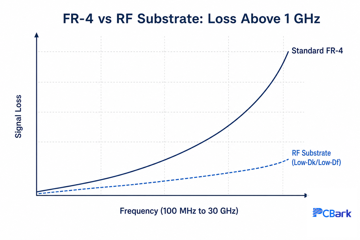
FR-4 doesn’t abruptly fail at one specific frequency—it degrades continuously through two dielectric materials properties every PCB engineer should track: dielectric constant (Dk) and dissipation factor (Df). Whether that degradation disqualifies the material depends on the design’s loss budget, not on crossing a fixed GHz threshold.
Peer-reviewed antenna research has shown FR-4 boards performing fine in limited applications up through a few GHz, including a published ultra-wideband antenna design measured from 980 MHz to 4.2 GHz. Much as with digital design, the cumulative effect of loss means a design crosses a failure threshold that varies with its specific loss budget rather than a clean cutoff point. A short, narrowband antenna feed will hold a precise signal at a higher frequency than a microwave tight-spiral feed will, which is exactly the kind of loss-budget-dependent judgment call NASA’s own High-Speed PCB Design Guide walks engineers through rather than offering a single frequency cutoff.
Dk governs the speed of the electromagnetic wave through the dielectric and, along with trace geometry, sets the impedance that keep a signal precise and minimal in loss rather than smeared and scattered. Published datasheets for FR-4 put Dk at about 4.3-4.8 at 1 MHz, but that number isn’t stable across frequency—most manufacturer data shows it drifting downward toward the 3.9-4.2 range by 10 GHz, though independent measurements vary by grade and test method (some published microwave-band measurements report FR-4 Dk closer to 4.5-4.8 with meaningful test uncertainty, underscoring that a single generic “FR-4” datasheet number should not be trusted at RF frequencies without confirming it against your specific laminate lot). If a design used only that 1 MHz figure, the real-world impedance will differ, and every connector, via, and layer transition becomes a tiny impedance discontinuity that reflects part of the wave back toward the source.
📐 Engineering Note
The Df of typical FR-4 approaches 0.02, or roughly 10-20× worse than pure PTFE (0.0009-0.002). Since insertion loss is proportional to Df frequencys, that same trace length that lost maybe a tenth of a dBon a board with zero losswill lose five or ten times more in the microwave. That loss contributes directly to range, to SNR, and to the amount of work the power amplifier must do to deliver an equivalent output.
To make the trade-off concrete, consider two identical antenna feed traces, one on an FR-4 and the other on a PTFE laminate, both feeding a 24-GHz automotive radar front end. Over a 2-in. feed line, the FR-4’s higher Df cuts into the link budget by enough to decrease the detection range; on the PTFE trace, it preserves the budget the radar algorithm was designed around. This is a real, measurable difference in a link-budget-limited design-but not a universal one. A short FR-4 trace to a narrowband 2.4-GHz antenna that stays well within the loss budget is fine-exactly what the published antenna research shown previously implies. The dividing line isn’t a frequency number, but rather whether the loss budget of the design at hand can accommodate the higher Df of the FR-4. That’s why material selection (covered below) is a budget equation, not a frequency lookup table.
RF PCB Design Rules: Impedance Control, Trace Routing and Via Strategy
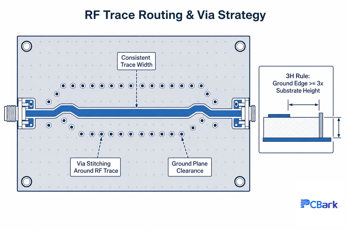
Once the material choice is made, the layout must carry its share of the load. Four guidelines stand between a board that meet its specified frequency and one that grapples with signal integrity problems through out its debugging cycle: impedance control, trace routing discipline, via minimization, and stack-up symmetry.
What Does Impedance Control Mean and Why Does It Matter?
Impedance control means holding a trace’s characteristic impedance—50 ohms single-ended or 100 ohms differential is standard for RF work—within a tight tolerance for the trace’s entire length. If impedance varies, part of the signal reflects back instead of reaching the load, showing up as insertion loss, ringing, or a distorted signal on the receive path.
Common practice converges on a ±10% controlled-impedance tolerance on production boards, tightened to ±5% or even ±3% when the design’s link budget has very little margin to spare, based on references across several independent PCB vendors rather than a claim from a single one.
📐 Engineering Note — Worked Example
The simplified microstrip characteristic-impedance formula, standard in RF engineering references, is:
Z (87 (Dk + 1.41)) ln(5.98h (0.8w + t))
where h is substrate height, w is trace width, and t is copper thickness (all in the same units). This equation works reasonably well for Dk in the 2-6 range and w/h ratios between about 0.1 and 2 (typical for microstrip). For standard 1.6-mm FR-4 (Dk=4.5, h=1.6 mm, t=35 µm [1 oz] copper) to achieve a 50-ohm target impedance, you’d calculate a required trace width of approximately 2.9 mm, according to several independent PCB design references. Shift only the substrate material to a PTFE laminate (Dk=2.2), keeping everything else the same and maintaining the 50-ohm target, and you’ll find the required trace width narrows-a lower Dk raises the impedance for any given geometry, and thus traces must be either narrower or wider depending on whether you’re solving for w or h. You must make this calculation before designing your stack-up, not after the board return from fabrication—the kind of characterization work that underlies real RF laminate patents such as US11996473B2, which documents large-signal RF characterization on high-frequency laminate before a design ever reaches production.
Routing design runs on that same physics. When PCB traces carry RF or microwave signals, keep them short and as straight as possible to reduce crosstalk-each turn is a minor discontinuity and each added via a small inductive and capacitive jump that can reflect signal energy and perturb the PCB impedance. Where the above can’t be avoided in a dense circuit layout, placing via stitches in ground and power around the signal path (grounding vias spaced at a fraction of the signal wavelength) will maintain the return-current path and can reduce radiated EMI measurably. The basis that allow all of this to be done in production (rather than just in the lab prototype) is a symmetric stack-up with ground and power layers positioned adjacent to each signal plane.
Setting Up Controlled Impedance in Common EDA Tools
The question engineers migrating from general digital layout to RF often have first is: “How do I implement these rules in the CAD tool I prefer?” (In Altium Designer, you configure controlled impedance profiles on a per-layer basis within the stack-up manager, and these profiles then influence width calculation in the autorouter when tagged nets are present. KiCad addresses this functionality with its internal transmission line calculator, passing trace-width recommendations to its interactive router. In either case, you must start with accurate Dk and copper roughness numbers-poor stack-up input means confidently inaccurate impedance results. Therefore, the worked example in this manual is still a good one to verify in which ever tool eventually lays out your board—treat it as a baseline high frequency PCB design guideline check, not a substitute for the tool’s own field solver.)
Material Families for High-Frequency PCBs: PTFE, Ceramic-Filled Hydrocarbon and Hybrid Stack-Ups
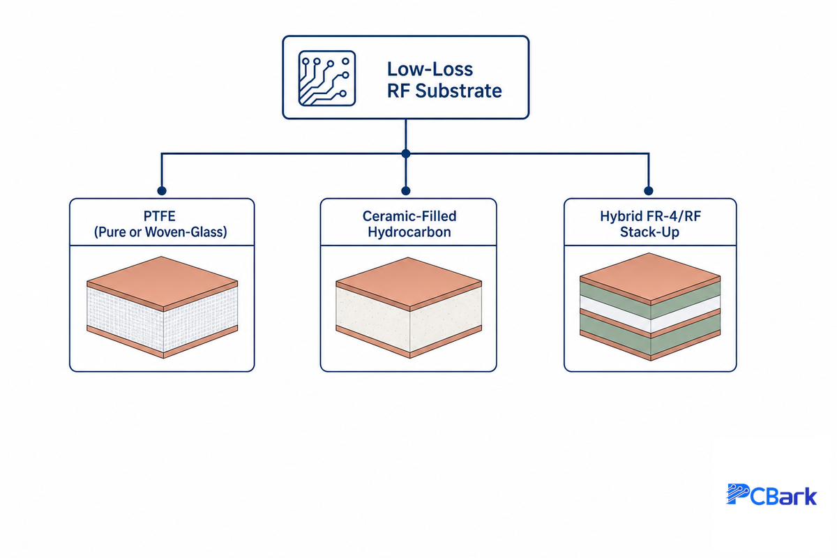
IPC-4103B, the base materials spec for high-speed and high-frequency applications, defines brand name RF/microwave laminates – for instance, Panasonic’s Megtron series or Rogers – in only a few familiar families based on low dielectric loss, rather than just a big list of names. The family structure allow an engineer selecting PCB material for high frequency applications to make an initial, “ballpark” choice before even grabbing a datasheet.
| Material Type / Property | Pure PTFE | Ceramic-Filled Hydrocarbon | Glass-Reinforced Hydrocarbon | Hybrid FR-4/RF Stack-Up |
|---|---|---|---|---|
| Typical Dk | 2.1–2.6 | 3.0–3.5 | 3.3–3.8 | 3.5–4.5 (blended) |
| Typical Df (loss) | 0.0009–0.002 | 0.002–0.004 | 0.003–0.006 | Varies by layer |
| Processing Difficulty | Highest — plasma etch/specialized drilling required | Moderate — closer to FR-4, better dimensional stability | Low-moderate — closest to standard FR-4 | Moderate-high — lamination compatibility is the main risk |
| Relative Cost vs. FR-4 | Highest (top of 5–15× range) | Mid-range | Lowest of the four | Mid-to-high (RF layers only) |
| Dimensional Stability | Lower — softer material moves more under lamination | Good | Good | Depends on CTE match between layers |
| Frequency Ceiling (practical) | Highest — mmWave-capable | To ~40 GHz typical | To ~10 GHz typical | Limited by the FR-4 portion of the design |
| Typical Fit | mmWave, satellite, lowest-loss requirements | 5G mid-band, automotive radar, general RF | Cost-sensitive RF below ~10 GHz | Mixed digital+RF boards |
| Governing Spec | IPC-4103B | IPC-4103B | IPC-4103B | IPC-4103B + IPC-2221C |
| Example Brand Families | RT/duroid-class laminates | Rogers RO4000-series, Megtron | Rogers RO3000-series-class | Mixed per stack-up design |
✔ Pure PTFE Advantages
- Lowest available dielectric loss (Df as low as 0.0009)
- Best choice when link-budget margin is thin
- Stable Dk across a wide temperature range
⚠ Pure PTFE Limitations
- Highest material cost of the four families
- Requires specialized drilling/plating process control
- Softer, more dimensionally sensitive during lamination than ceramic-filled options
Copper foil roughness and manufacturability also factor into this decision: a finer grain size gives rolled copper a smoother surface finish, which cuts conductor loss at microwave frequency but raises processing cost, another case where materials with low dielectric loss aren’t automatically the obvious pick just because their Dk is lowest. The more critical selection error is picking a material for its low Dk alone because “lowest loss is always best.” According to Altium’s own guidelines on their range of RF substrate materials such as Rogers laminates, you don’t always need the lowest Dk, and independent industry guidance on RF materials confirms the need for additional selection parameters beyond a single number on a datasheet chart—the same multi-parameter thinking behind NASA’s own qualification approach in GSFC-STD-8001, which qualifies high-frequency materials on more than one property. If you choose the material based solely on the lowest Dk, you would never choose frequency alone, ignoring as it does the associated cost and thermal expansion properties, or whether a component would behave no different if placed on an inexpensive ceramic-filled hydrocarbon, given the overall requirements for loss performance of the system link budget.
The Signal-Loss Tolerance Triage
4-step question flow for reducing material families before selecting datasheets:
- What’s the real operating ceiling? Under ~6 GHz for reasonable link budgets glass-reinforced hydrocarbon does the job and no reason to always use PTFE.
- How thick is the link-budget margin? A radar or satellite link that barely has any margin is certainly worth the extra cost for PTFE’s low Df, whereas a Wi-Fi front-end that has a couple of dB to play with typically doesn’t.
- Is it possible to mix digital and RF in one PCB? If it’s then a hybrid FR-4/RF stack-up is a good way to not pay PTFE for the whole panel.
- What’s the production volume and drilling/plating capability of the fabricator? PTFE’s process difficulty is a real cost and yield factor at volume, not just a datasheet footnote.
For a deeper, grade-by-grade comparison of specific Rogers laminate families-RO4000-series versus RO3000-series versus PTFE/RT-duroid options, with full Dk/Df tables and IPC-4103/IPC-6018D qualification detail-see our companion guide on Rogers PCB material selection. Where a project’s thermal or power-density requirements push past what any organic laminate can handle, ceramic PCB substrates are the next material family up the performance ladder. And once you’ve a material family shortlisted, PCBark’s own RF and microwave PCB manufacturing capabilities page details which specific frequency bands, layer counts, and impedance tolerances are production-ready today.
Fabrication Process: How Manufacturing RF PCBs Differs From Standard Boards

Material choice cascades into the fabrication process itself. PTFE and ceramic-filled laminates don’t etch, drill, or plate like FR-4-they require process adjustments a standard FR-4 line isn’t set up to handle.
PTFE’s soft, low-surface-energy nature resists standard electroless copper plating; fabricators run a plasma or chemical etch-back step first to roughen the hole walls enough for reliable adhesion, and skipping or under-running that step is a documented source of via reliability failures. Drilling parameters also shift: PTFE and ceramic-filled composites are more abrasive and heat-sensitive than FR-4, so drill bit selection, speed, and feed rate are tuned differently to avoid smearing resin across the hole wall (which then blocks the plating step that follows). Multi-material hybrid stack-ups add a third variable-registration between dissimilar laminates during lamination has tighter tolerance requirements than an all-FR-4 (FR4) stack-up, because each material’s coefficient of thermal expansion differs, so they don’t expand and contract identically under lamination heat and pressure or during frequency transmission testing afterward.
NASA’s own lessons-learned guidance on building reliable circuit board assemblies makes the same point from the fabrication side: skip the etch-back step on a PTFE panel and the result is not a subtle yield dip: plating adhesion fails at the hole wall, and a batch that should have cleared inspection at better than 98% first-pass yield can come back with double-digit via-reliability rejects instead. None of this is exotic for a circuit fabricator set up for it, but it explains why RF and microwave board quotes rarely match standard FR-4 turnaround times or yield assumptions-the process controls that prevent via failures and registration drift add real steps, not just a different bill of materials. PCBark’s own production line, for example, runs frequency-band-tiered capability from 1-6 GHz through 6-40 GHz up to 77+ GHz specifically because each tier requires a different combination of drilling parameters and etch-back process control-a single generic “RF process” doesn’t cover the full range, which is why asking a fabricator which specific frequency tier their process qualifications cover is a more useful question than asking whether they “do RF boards” at all.
Applications: 5G, Radar, Satellite, Aerospace and Medical Systems
high-frequency PCBs concentrate in applications where signal loss directly costs range, resolution, or reliability-not just data rate.
A typical example are radar systems automotive solutions built around a 77-81 GHz collision-avoidance radar module: the antenna feed network is right on the board, so every dB of insertion loss from the PCB itself bites into detection range and false-alarm margin. Ceramic-filled hydrocarbon or PTFE laminates are used for automotive radar, and for good reason-in 24 GHz and 77-81 GHz bands, there’s little room to absorb the Fr-4 equivalent loss and boards must maintain their parameters across automotive temperatures (-40°C to 125°C is common) with the impedance drifting no more than specified.
The demand for high-frequency 5G technology is a driver for some of today’s most novel high-frequency applications. The infrastructure supporting 5G spans the entire spectrum, with sub-6 GHz base station boards with high-speed data transmission capabilities benefiting from ceramic-filled hydrocarbon laminates, while 28-39 GHz mmWave small-cell antenna arrays move toward PTFE for the lowest possible loss, using wireless links that leave little room for error. PTFE is generally preferred in satellite communications applications (both on the ground segment and in payload) because signal budgets over satellite links offer virtually no tolerance for wasted dielectric loss. Aerospace applications, especially advanced defense radar and avionics, add the stringent IPC Class 3 reliability requirements to guarantee both performance and reliability over the platform’s service life, and for this reason, NASA’s own board standard, GSFC-STD-8001, dedicates a chapter to high-frequency/microwave technologies instead of lumping it under general design standards. Medical imaging systems, including radio frequency (RF) enabled diagnostic tools, use high-frequency designs for imaging front-ends that require very clean signal transmission for overall image fidelity rather than throughput.
Standards and Compliance: IPC-2221, IPC-4103 and Testing
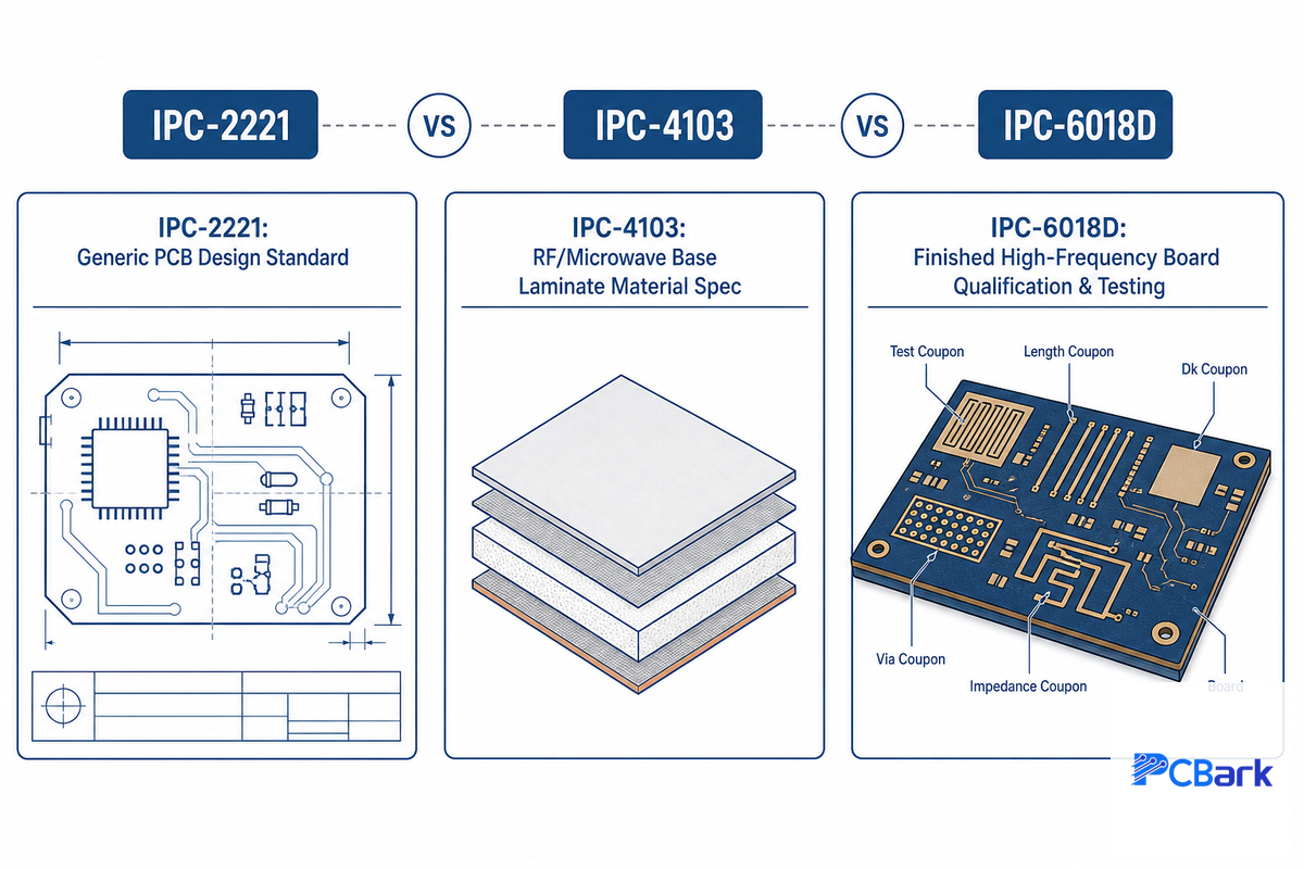
There are three IPC standards used in RF and microwave PCB design and qualification, which represent distinct areas of consideration and shouldn’t be confused: a supplier who waves a generic “IPC certified” claim without naming which of the three applies is a real red flag, not just an imprecise answer, because a board that passes IPC-2221C’s general design rules can still fail IPC-6018D’s microwave-specific qualification testing—precisely the layered-standards approach NASA takes in GSFC-STD-8001, which treats general and high-frequency board qualification as separate requirement sets.
IPC-2221C, revised in December 2023, is the general printed board design standard addressing conductor spacing, current carrying capacity, and common layout guidelines regardless of signal type, serving as a base layer for all printed boards. IPC-4103B is the material standard; it lists and characterizes various types of laminates including PTFE, ceramic-filled hydrocarbon and glass-filled hydrocarbon as noted previously for high-speed and high-frequency applications and enables fabricators to identify a specific type of PTFE, rather than using a broad generic designation. IPC-6018D, a revision from February 2022, is a high-frequency (microwave) qualification and performance standard specific to high-frequency printed boards, applicable to microstrip, stripline, and mixed dielectric designs, and providing acceptable criteria beyond the more general rules specified in IPC-2221C.
IPC-6018D, rather than IPC-2221C, dictates the actual testing and validation. Controlled impedance is evaluated by time domain reflectometry (TDR), which measures signal reflections off discontinuities along a trace-like vias or layer transitions-that a standard continuity check would miss. Critical applications such as defense, aerospace, and automotive radar applications requiring IPC Class 3 often have plating thickness, annular ring, and cleanliness tolerances beyond commercial IPC Class 2.
PCBark’s manufacturing experience itself – more than 16 years with the company and IPC-A-610 class 2 & 3 certification and the ISO 9001/IATF 16949 quality systems – is founded upon this very standard stack as described on our company background page. That’s why the specific number above is what to request of any potential RF PCB manufacturer rather than an unqualified claim of “IPC Certified.”
What Drives High-Frequency PCB Cost
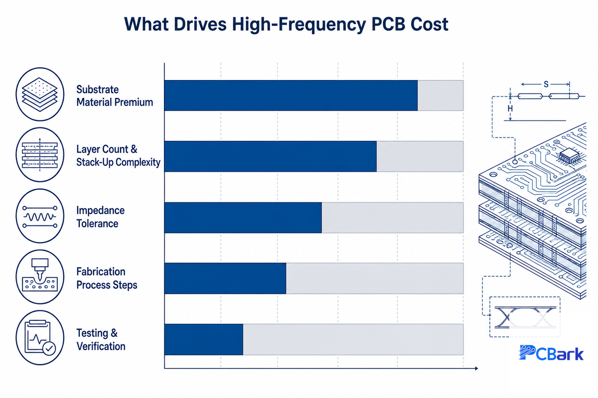
Industry estimates put RF and microwave boards, built on microwave laminates instead of common FR-4, at roughly 5x to 15x the cost of an equivalent FR-4 board (an order-of-magnitude approximation from public fabricator price lists, not an independent market study). Four cost factors stacking multiplicatively account for that wide range.
That multi-factor pattern echoes the yield-and-process-control cost drivers documented in NASA’s own circuit board lessons-learned report: material cost, process yield, tolerance requirements, and production volume each move independently.
Key Cost Factors
- In fact material-industry published data indicates PTFE and ceramic-filled laminates costs range $2-$10 per square inch, compared to $0.10-$0.50 for FR-4, which is an order of magnitude difference even before anything gets started.
- 119Process yield – the process etch-back, offset drilling and closer registration controls discussed in the above process steps add process complexity and risk of scrap, which aren’t found on FR-4 lines.
- impedance tolerance-tightening from ±10 percent to ±5 percent or ±3 percent increase the test-and-rework overhead because more boards miss the tighter acceptance band.
- These higher relative per-board fixed cost implications from volume-prototype and low-volume RF runs, though inherent to PCB fabrication as a rule, can be accentuated if specialty material handling is required.
This is a directionally pricing for the industry; a quote is actual, not per unit price, for specific material grade, layer count, panel utilization. And price changes based on current copper and laminate raw materials market. A fastest quote is based on your chosen material family (from the above triage), you could refer to PCBark’s RF and microwave PCB manufacturing page which lists all frequency bands, material options, layer counts in production to get a project specific price.
Common High-Frequency PCB Design Mistakes Engineers Make
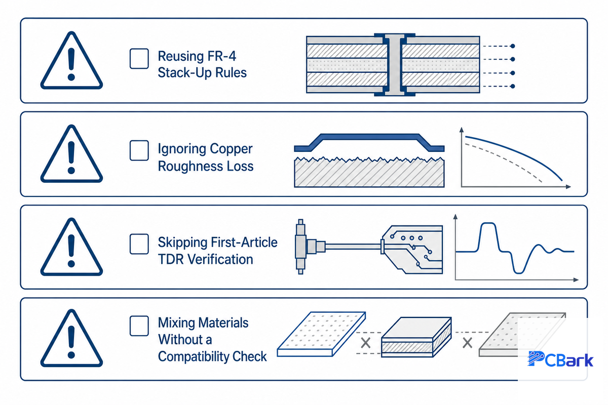
“Frequency alone is a bad RF PCB material selection criterion, the lowest-Dk option is not always the lowest-loss choice once you account for how the rest of the stack-up behaves.”
paraphrased from independent RF materials-selection guidance (Altium resources), consistent with practitioner discussion in engineering forums
Beyond the Dk-fixation mistake above, engineers transitioning from general high frequency circuit design into RF-specific layout fall into a handful of similar avoidable mistakes documented in engineering post-mortems such as NASA’s circuit board assembly lessons-learned report—and each one is a real board respin, not a theoretical risk. Overusing vias on signal paths is far and away the most prevalent-every time a high-frequency trace has a via through it, it introduces inductance and a slight impedance step, and RF layouts are about minimizing the number of vias on critical nets, not throwing them on like a digital bus. Close behind is ignoring return-current paths: when a signal layer is devoid of a continuous, immediately adjacent ground plane, return current has to find a longer, winding path, which radiates as electromagnetic interference (EMI) and degrades signal integrity in ways that are hard to trace back to the layout decision that caused them. Under-spacing parallel traces invites crosstalk that a digital designer might let slide but an RF system can’t, when energy couples between adjacent high-frequency traces, it appears as spurious signal reflections, and minimal signal degradation compounds quickly in the receiver chain. Evidence of this steep learning curve is easily seen on any online forum discussion of first-time RF PCB development by embedded engineers (r/embedded), where almost universally participants significantly underestimate the extent to which layout discipline-beyond mere material selection-will decide whether a given RF board will work on the bench.
Industry Outlook: What’s Changing in High-Frequency PCB Materials
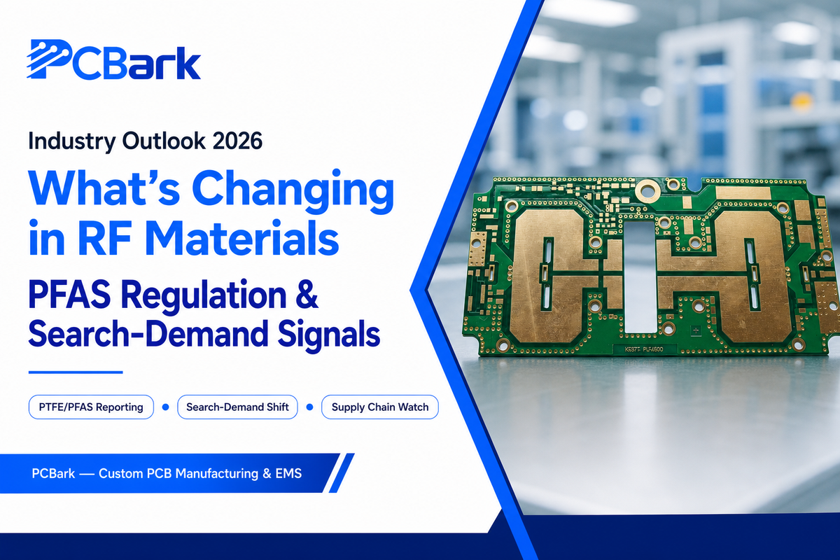
(Updated July 2026) The nearest-term driver in this category is less about predicting the size of a market and more about watching what engineers are actually searching for. Searches for terms like PTFE PCB and Teflon PCB material spiked 40-75% year over year into mid-2026, out performing the broader “RF PCB” search terms which were flat to slightly down in the same timeframe. That gap indicates where interest is actually concentrating-on the very top performance tier of materials, not just RF boards more generally-and it lines up perfectly with what we’re seeing in 5G mmWave and automotive radar programs as they ramp into production from pilot volumes and need true PTFE-grade loss performance and a low loss factor to meet link budget targets on the resulting high-frequency boards.
A second driver for this market trend is a regulatory one, rather than technical, and is one that’s easier to overlook, since it isn’t mentioned in typical RF performance discussions: PTFE is a fluoropolymer, one of the chemical compounds commonly referred to as PFAS. As of October 2023, the EPA published its PFAS Reporting Rule under TSCA Section 8(a)(7), mandating that anyone who has manufactured or imported PFAS since 2011 must submit a report (a rule that applies directly to importers of PTFE-substrate PCBs). In November 2025 the EPA separately proposed restricting the scope of the reporting rule to exclude low-concentration and article imports, which may apply to some of those same PTFE PCBs, and the submission period itself has slipped repeatedly—most recently pushed from an April 13, 2026 start to January 31, 2027 (or 60 days after the final scope revisions take effect, whichever is later). For those working on programs that require PTFE substrate, monitoring these supply-chain and compliance issues in parallel with material selection, and understanding any separate PFAS requirements in specific industries or geographies, is prudent.
Practical consequence of designing from today forward: if a roadmap has a mmWave variation as little as 12-18 months out, it’s worth vetting both a realistic upgrade path to PTFE and the current status of supply chain’s PFAS reporting (not finding these out during production ramp). The overall PCB market size forecasts (the larger category with mid-single-digit to high-single-digit growth in the tens of billions through the early 2030s) are directionally consistent, but serve as context, not justification for making a material decision. Instead, the search-demand, application-adoption, and regulatory signals are the more pertinent view of where the category is going.
Q: What is a high frequency PCB?
View Answer
A high-frequency PCB (also called a high-frequency circuit board) is a board built with low-loss substrate materials—typically PTFE, ceramic-filled hydrocarbon, or hybrid FR-4/RF laminates—in place of standard FR-4, so RF, microwave, and millimeter-wave signals maintain high signal integrity and lose minimal energy crossing the board. This differs from a “high-speed PCB,” covered above. The category generally starts around 100 MHz to 1 GHz, depending on the source.
Q: What is a Rogers PCB?
View Answer
Rogers PCBs are PCBs manufactured with laminates supplied by Rogers Corporation, a leading manufacturer of ceramic-filled hydrocarbon and PTFE-based high-speed and high-frequency PCB materials (e.g., the RO4000 and RO3000 product series). Rogers has almost become a genericized trademark for high-frequency laminates, similar to Kleenex for tissue, but it’s just one manufacturer among the material categories we discuss below. Other qualified suppliers include Taconic, Isola, and Arlon — consult our Rogers PCB guide for grade-specific details.
Q: What are the three types of PCBs?
View Answer
By construction, there are three categories of PCBs: rigid, flexible and rigid-flex. By number of layers, these are single-sided, double-sided, or multilayer. None of these definitions is exclusive to high-frequency PCB technology; an RF/microwave design can be made in rigid, flexible, or rigid-flex formats and can have a single layer, two layers, or many layers.
Q: What is the 3H rule in PCB?
View Answer
The 3H rule is a layout guideline for high-frequency PCBs: keep the nearest ground plane edge or split at least three times the substrate height (h) away from any high-frequency trace or via, to limit fringing-field coupling and impedance shift.
Q: Can high-frequency materials be combined with FR-4 in one stack-up?
View Answer
Yes, these are the hybrid FR-4/RF stack-ups discussed above. RF sections (PTFE or ceramic-filled hydrocarbon) layer together with conventional digital FR-4, so only part of the board’s layers carry the material premium. The trade-off is added lamination-compatibility work, since FR-4 and RF laminates cure at different temperatures and have different z-axis CTE, versus an all-RF or all-FR-4 stack-up. This approach fits boards with limited RF circuitry alongside substantial digital segments, usually at lower cost than an all-RF stack-up.
Q: What is the procedure for ordering a high-frequency PCB with an impedance specification?
View Answer
Give your fabricator the target impedance, tolerance (typically 10%, 5%, or 3%), material family or laminate grade, and trace/space geometry. A quality fabricator returns a stack-up confirmation with revised trace widths and runs first-article TDR verification before production.
See PCBark’s RF & Microwave PCB Manufacturing Capabilities →
Why We Write This
PCBark’s Technical Team writes this guide from 16+ years fabricating RF and microwave PCBs, checking every frequency band spec against IPC-2221C, IPC-4103B, and IPC-6018D standard text plus NASA’s GSFC-STD-8001 quality standard. Some figures here are directional data from a single commercial source rather than an exact measurement, and the draft was reviewed in full by the PCBark Technical Team before publication.
References & Sources
- IPC-2221C Generic Standard on Printed Board Design — IPC International
- IPC-4103B Specification for Base Materials for High Speed/High Frequency Applications — IPC International
- IPC-6018D Qualification and Performance Specification for High Frequency (Microwave) Printed Boards — IPC International
- GSFC-STD-8001: Standard Quality Assurance Requirements for Printed Circuit Boards — NASA Goddard Space Flight Center
- High-Speed PCB Design Guide — NASA
- Microstrip Impedance Reference — Microwaves101 (IEEE MTT-S affiliated engineering reference)
- What Makes RF PCB Design and Manufacturing So Complex — Microwaves & RF (MWRF)
- Design Considerations for High Reliability RF PCB Circuit Designs for Extreme Environments — Microwave Journal
- Basic Concepts of Designing an RF PCB Board — EDN
- US11996473B2, Flexible transistors with near-junction heat management — USPTO / Google Patents
- TSCA Section 8(a)(7) PFAS Reporting and Recordkeeping — U.S. Environmental Protection Agency
- PFAS Data Reporting and Recordkeeping Under TSCA — Federal Register, November 2025
Related Articles
- Rogers PCB Material Selection Guide — Dk/Df tables and grade comparison
- Ceramic PCB Guide — materials, bonding methods and reliability testing
- Heavy Copper PCB Guide — manufacturing process and IPC standards
- Aluminum & Metal-Core PCB Guide — thermal design fundamentals
- PCBark RF & Microwave PCB Manufacturing Capabilities



![16-24 Layer PCB: Stackup, Lamination & Design Guide [2026]](https://pcbark.com/wp-content/uploads/2026/07/16-24-layer-pcb-guide-featured-2-150x150.png)


