Get in touch with PCBark Company


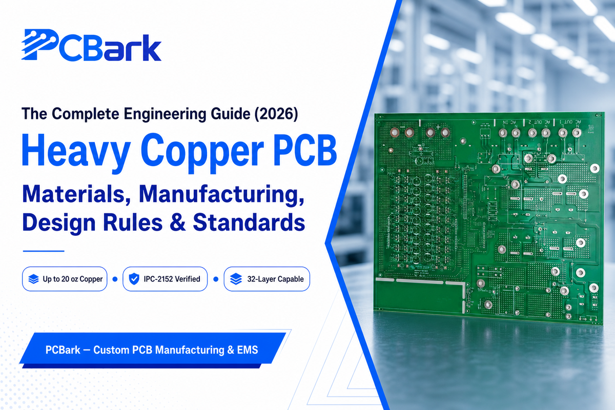
heavy copper pcb. A heavy copper pcb is a printed circuit board constructed using copper weights far heavier than the 1-2 oz found in standard boards. The material, process, and standards selection process makes the difference between a board that meet its design life and a board that will crack at the plated-through holes. The following guide examines heavy copper boards-the definition, fabrication, and specification of them; the equivalents in both copper weight and thickness; the laminate and foil used; the changes in manufacturing once copper is thick; IPC-standard calculations for trace sizes; standards and classes of acceptance; reliability tests, real-world applications logic, and the pitfalls most commonly experienced during the first heavy-copper design project.
In short: A heavy copper pcb in industry-speak is usually taken to mean a board with at least 3 to 4 oz/ft (105-140m) of copper on at least one layer – this can go up to 20 oz/ft and much more for ultra-copper builds. This added copper mass holds a lot more current and dissipates heat better as well as resisting cracking from thermal cycling compared to the typical 1-2 oz copper of a standard board.
Quick Specs
| Heavy copper range | 3-20 oz/ft² outer layers (105-700 µm) |
| Extreme copper range | Above 20 oz/ft², up to 200 oz/ft² |
| Governing standards | IPC-2152, IPC-2221, IPC-6012, IPC-A-600, IPC-9701 |
| Typical inner-layer derating | ~50% of external-layer current capacity (approximation, see H2-5) |
| PCBark fabrication range | 2-20 oz outer / 2-12 oz inner, up to 32 layers, up to 6mm board thickness |
What Is a Heavy Copper PCB?
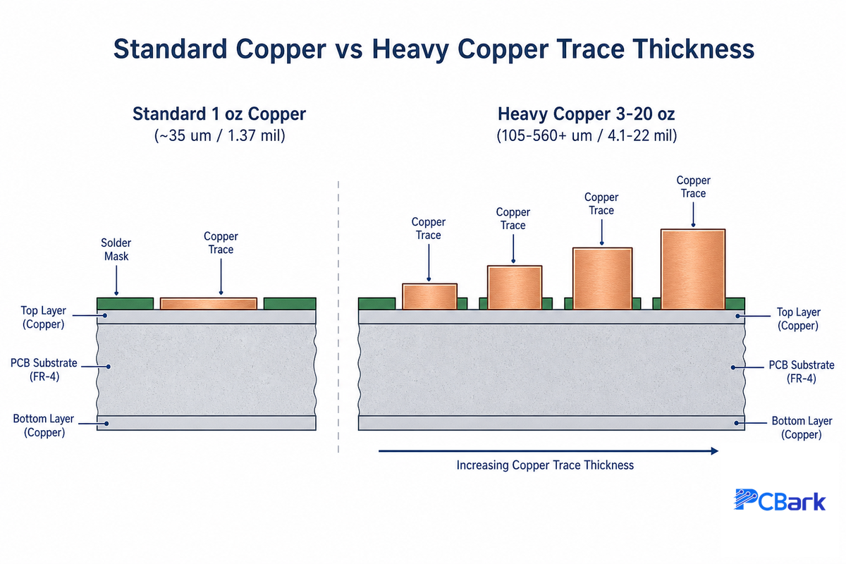
There’s no single document, identifiable by IPC number, that declares a specific gram weight, labels it heavy copper, and sticks a fork in it. That fact disorients engineers accustomed to tracing every bit of the PCB lexicon back to a standard’s precise clause. Even Sierra circuits’ own knowledge base takes a refreshingly direct approach: “there are no definite rules that specify the amount of copper to be used when fabricating heavy copper boards,” while noting the common understanding in the industry that “any layer 3 oz/ft² and above is referred to as heavy copper.” Epec Engineered Technologies pushes the standard back an ounce. They categorize their commercial boards as operating between 0.5 to 3 oz/ft², their heavy copper at 4 to 20 oz/ft², and any thing over that to 200 oz/ft² is dubbed EXTREME copper. Yet another definition can be found in the knowledge base at PCBGoGo, where “thick/heavy copper” is defined as finished copper over 4 oz (140 µm). All of these definitions are correct, as each fabricator is simply drawing a line on the “conventional” chart at a slightly different place since no IPC standard itself uses the term “heavy copper.”
Whether a datasheet call it a heavy copper circuit board, a heavy copper printed circuit, or, at the extreme end, an extreme copper printed circuit board, the underlying physics is identical: more copper printed circuit mass carries more current and spreads more heat. Engineers sometimes shorten the term to heavy Cu on drawings and quote requests. What all the sources concur on is the physics behind the problem: if the design requires the ability to carry more current, dissipate more heat or handle more mechanical stress on the pad or in the plated hole of a 1-2 ounce per foot foil than is possible with such copper, the solution is to use a thicker layer of copper – not to widen the trace in the 1-2 oz per foot layer. That’s the essence of the “heavy copper” and the reason that a 3-4 oz per foot foil is the initial point from which the industry starts – that’s how much copper fabricators see that requires new methods of plating and etching (see H2-4). Academic treatment of the underlying physics goes back decades — see this IEEE analysis of current-carrying capacity in PCB traces for the classical derivation that heavy-copper practice is built on.
What Is the Difference Between Heavy Copper and Extreme Copper PCBs?
Heavy copper usually refers to 3-4 oz/ft² to about 20 oz/ft² where your standard etch-only fabrication isn’t a practical solution, and step-plating or differential etching becomes a requirement. Above roughly 20 oz/ft² to about 200 oz/ft², you’ve moved into EXTREME copper territory. At that thickness, you’re doing much more than just routing power on a trace, you’re designing on-board heatsinks out of the surface, making planar transformer windings from flat copper sheet instead of wire, and creating in-board high-current busbars instead of bolted-on copper plates. The underlying process technologies are still similar (step plating, differential etching, balancing copper on each layer, etc) to heavy copper but taken further so the practical difference between heavy and extreme is less about regulation and more about how you manage the fabrication process.
Copper Weight & Thickness: The Full Reference System
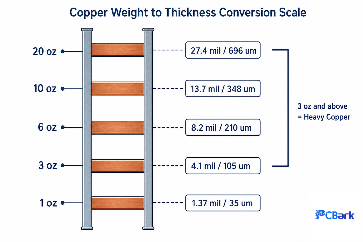
This reference system is applied regardless of whether you’re building a board with 1 oz of copper or 20 oz of copper because the conversion math for printed circuit will never change based on copper weight. copper weight is defined as oz/ft. this is a carry over from the historical practice of defining copper weight by its density before rolling it out and plated it into whatever thickness required. Physics fixes that conversion: one ounce of copper evenly spread across a 1-foot square has a thickness of 1.37 mils (0.00137 in) which is equal to 34.8 µm (more commonly approximated as 35 µm). All other weights are a linear function of this base constant, which is why the table below is a direct lookup.
| Copper Weight (oz/ft²) | Class | Thickness (µm) | Thickness (mil) |
|---|---|---|---|
| 0.5 oz | Standard | 17.4 µm | 0.69 mil |
| 1 oz | Standard | 34.8 µm | 1.37 mil |
| 2 oz | Standard | 69.6 µm | 2.74 mil |
| 3 oz | Heavy (convention floor) | 104.4 µm | 4.11 mil |
| 4 oz | Heavy | 139.2 µm | 5.48 mil |
| 6 oz | Heavy | 208.8 µm | 8.22 mil |
| 10 oz | Heavy | 348.0 µm | 13.70 mil |
| 20 oz | Heavy (top of range) | 696.0 µm | 27.40 mil |
| 30-200 oz | Extreme copper | 1,044-6,960 µm | 41.1-274.0 mil |
If you want to skip the math altogether and calculate a specific trace, PCBark’s copper thickness converter (oz · µm · mil) is handy for this. This table serves as the working reference document for the heavy-copper designation, not a deep dive into trace-width and current-capacity calculations (see H2-5) which are unrelated to simply finding the physical thickness of a particular oz of copper.
📐 Engineering Note
A 1 oz = 1.37 mil constant is only true for perfectly flat and evenly-plated foil. Heavy copper substrates seldom have perfectly flat etched and plated results, with etching/plating tolerance often at 10-20% at 3oz and up – it’s another reason why fabricators list a minimum finished copper rather than an exact value.
Materials Science: Copper Foil Types & Laminate Selection
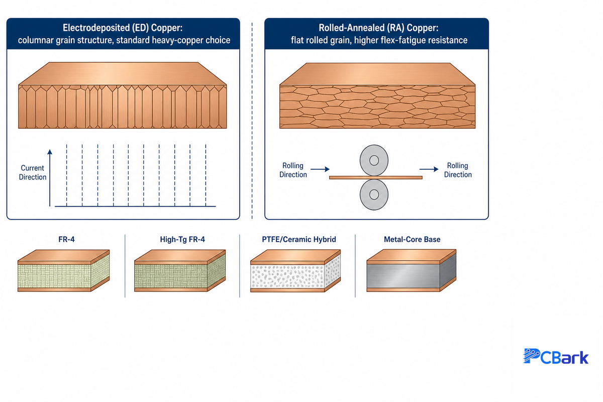
There are two major underlying assumptions in every heavy copper stack-up that rarely are discussed directly with the oz value itself. What’s the source of the copper (Cu) layer? And, under what board material is the Cu attached to the substrate, and what’s done to prevent warping? In either case, copper is the conductive element providing electrical conduction, and the dielectric material beneath it has to survive the same thermal and mechanical stress the thicker copper circuit is designed to handle.
How Copper Foil Is Made Copper foil used in PCB lamination comes one of two ways: • Electrodeposited (ED) copper is plated onto a revolving drum, leaving a columnar, nodular grain structure on the treatment side; this is the lower-cost, most widely used foil and is appropriate for the vast majority of heavy-copper board applications.
• Rolled-annealed (RA) copper is mechanically rolled and annealed to desired thickness, resulting in a finer, more uniform grain structure and greater ductility. RA foil is more expensive, and used only in select applications where boards will be subjected to frequent flexing, or when fatigue resistance at a via or fold line is a more critical concern than price; this has historically been the standard foil used for flex and rigid-flex circuit applications, and it’s occasionally used in heavy-copper applications where extreme thermal cycling is a primary concern, as ductility enables better thermal expansion and contraction at the vias without the same tendency to cause micro-cracks in the trace.
Laminate The material beneath the copper is just as important as the copper itself. Standard FR4 laminate has a maximum operating temperature rating of about 130°C, which generally exceeds the current of even many heavy-copper designs. However, for boards used in very high temperatures (e.g., under-the-hood applications or the area near a power supply’s heatsink) rather than the circuit’s current, the maximum ambient temperature to consider goes up to 250°C, in which case polyimide laminate must be used. For heavy-copper applications, the ultimate material consideration at the copper-laminate interface isn’t usually the thermal tolerance of the resin itself, but rather the mismatch of thermal expansion between the copper and the laminate. As the board is cycled up and down in temperature, the copper and standard FR-4 resin will expand and contract at different rates; this difference, known as CTE (Coefficient of Thermal Expansion) mismatch, is the force driving the nucleation of cracks in a plated-through hole during thermal cycling-a failure mechanism characterized by the IPC-9701 standard (H2-7) as part of the board’s design validation tests. Also, having a heavier copper layer serves as a passive heat dissipation component, helping dissipate heat from hot areas of the board, drawing heat towards cooler sections and reducing local hot spots, sometimes conducting heat to an external heatsink bonded to the board surface (a secondary effect of mass, completely independent of its current-carrying ability). In our heavy-copper work here at PCBark (from 2 to 20 oz on outer layers, to 12 oz on inner layers on boards as thick as 6 mm and up to 32 layers), selection of the appropriate laminates depends entirely on the projected real-world thermal cycling the end application will experience, rather than being based on standard practices. This is thermal management by mass rather than by airflow, and it matters most in electronic devices, power supply systems, industrial applications, and similar equipment, where a fan-cooled heatsink isn’t practical. An IEEE study of internal conductor current-carrying capacity documents the same heat-spreading effect from a materials-physics angle.
How Heavy Copper PCBs Are Manufactured
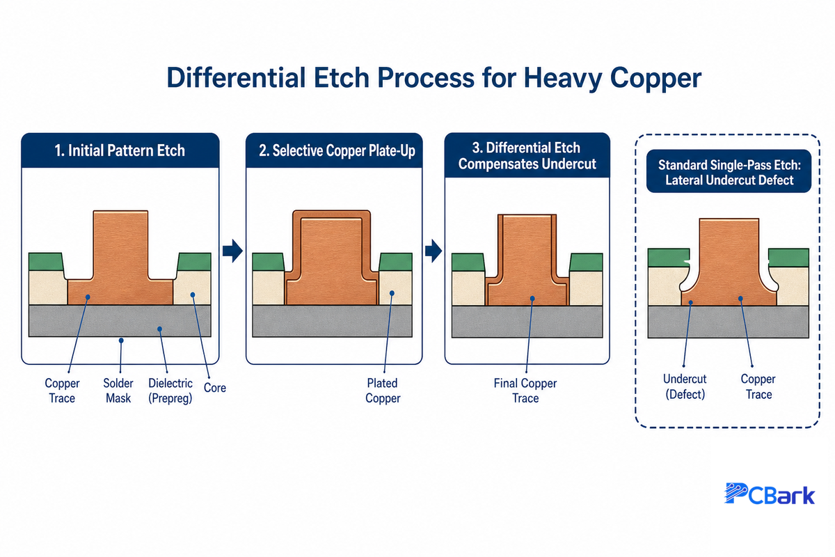
Each PCB, whether heavy copper or not, begins by laminating thin copper foil (typically 0.5-2 oz/ft²) to the base substrate, then removing portions of it by selectively etching, and in turn, selectively depositing more of it until the traces, planes, pads and plated-through-holes form the final circuit design. Once the desired thickness for heavy copper rises beyond the 3-oz/ft² range, a more advanced etching and plating process must be applied, the standard copper etching and plating processes used on 1 oz boards simply don’t scale, and fabricators rely on more advanced equipment to hold tolerance once copper gets this thick.
Subtractive etching physically dissolves the copper layer under the resist mask. It’s inherently isotropic, or attacks both vertically and horizontally with equal ease, to the point that the under cutting on a standard 1 oz layer is typically small enough to be negligible. On a 6 oz or 10 oz layer of copper, straight etching can result in a large undercut on a vertically defined trace, so the sidewalls will slope inward significantly, the feature size is unpredictable compared to what was originally drawn, and fine-pitch feature sizes can no longer be maintained within the tight tolerances of an industrial process. This is the differential-etch threshold – that point (generally somewhere around 3-4 oz for thick copper) at which the lateral undercutting caused by a single-pass etching pass has become too large relative to trace geometries and it becomes necessary for a fabricator to use some sort of controlled-plating in combination with a series of differential-etch passes.
For instance, a common way that thick copper features are built up is to have a normal, relatively thin base-copper layer etched by conventional techniques, then a portion of the thickness is plated selectively onto areas which need to achieve the thick-copper weight (referred to as “step-plating”), while differential-etching techniques are used to compensate for variations in the etching rates at various feature densities across the panel. For example, there’s a Chinese patent, CN105163523A, “Super-thick copper etching technique for PCB” that outlines a very similar technique for controlling sidewall profile on thick-copper products. Epec’s internal documentation of their own processes indicates that they previously would form the entire thick-copper traces by etching through thick clad laminate material, which led to the poor sidewall profile and undercutting, and they implemented combined plating and etching techniques which provide straight sidewalls with negligible undercut on heavy-copper designs. Getting this step wrong is a real risk for a first-time heavy-copper buyer: a fabricator that runs 6 oz copper through a standard single-pass etch line risks weeks of delay when the panel fails incoming inspection, because that process was never built around this much copper mass in practice. PCBark’s own heavy-copper production line has run differential etching and step-plating in-house for 16 years of production, precisely to avoid that failure mode.
Plating’s advantage over relying solely on etching is that fabricators can mix materials with vastly different weights within the same layer – e.g. 2 oz traces and 20 oz traces can be laid out side-by-side on the same plane – which allows for placing both high-frequency impedance traces and high-current power traces on the same layer instead of on two different layers (or boards). After the “thick-copper” plating is completed, heavy-copper boards are typically processed on standard SMT lines with one small adjustment; because of the larger copper mass acting as a heat sink, heavy-copper assemblies will tend to remove heat from the joint faster than standard boards, so a “longer soak time”, sometimes a higher “peak temperature”, in the solder reflow profile are needed to ensure the solder joints on or adjacent to the heavy-copper planes achieve adequate reflow, and aren’t a “cold” joint.
Current-Carrying Capacity & the IPC-2152 Design Method
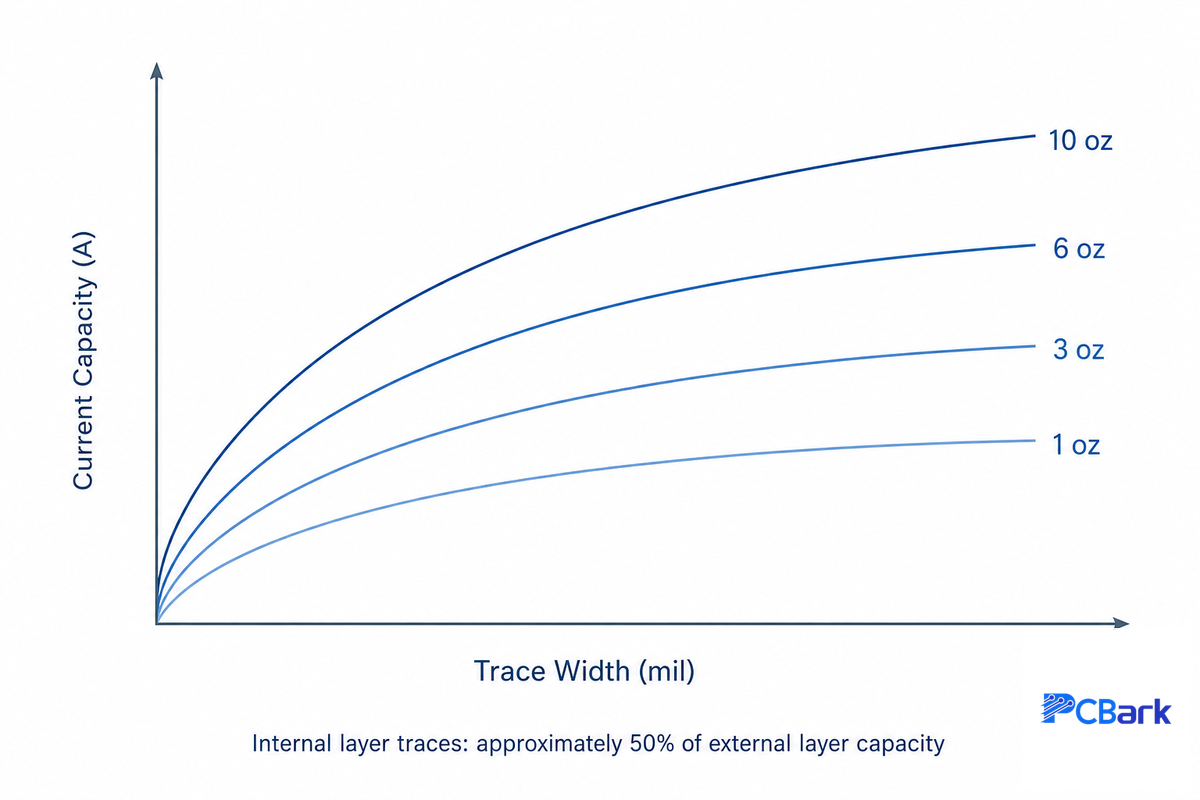
This is precisely the calculation to which heavy copper is designed to respond, and this is where a really useful distinction gets ironed into the usual marketing boilerplate in most PCB-fabricator material: the relative status of IPC-2221 and IPC-2152 is generally glossed over as “the new standard replaced the old standard.” If you consult the actual table of document revision in the ipc published material, that’s not precisely correct. IPC-2152, Standard for Determining Current Carrying Capacity in Printed Board Design, was originally published in August 2009 and hasn’t since been updated – its status on IPC’s table is shown as “No Longer Maintained” (which implies that no committee is currently working on updating the standard, but doesn’t mean the document itself is obsolete or defunct).IPC-2221, the standard that generically covers printed-board design, which includes the simpler, older charts, has actually seen a more recent update: Rev C came out in December 2023.
“…sets the sole industry standard for determining the appropriate sizes of internal and external conductors”
on IPC-2152, as reported in Circuit World, Emerald Publishing
In practice, both are still used today, and it would be most accurate to describe the relationship by scope rather than by age: IPC-2221’s charts are the quicker, more straightforward method most engineers default to first, and they are still current because IPC-2221 itself keeps getting revised. IPC-2152 is the more thorough, dedicated method for current-carrying capacity specifically, accounting for more variables, trace-to-trace spacing, board thickness, and conductor position among them, which is exactly why fabricator technical content (Cadence’s 2024 trace-thickness guidance, Sierra Circuits’ own IPC-2152 explainer, ANSI’s blog) keeps directing engineers to it for any but the most coarse initial estimate, though the document hasn’t been revised since 2009.
Worked Example: Sizing a 6 oz External Trace
From the IPC-2221A current-capacity relationship for an external trace: (I = 0.048 × ΔT0.44 × (W × Th)0.725) where ΔT is the maximum temperature rise permitted in °C, and W and Th are the trace width and copper thickness, respectively, in mils.
- Copper weight: 6 oz/ft² → thickness = 8.4 mil (referring to the table above)
- Trace width: 0.25 in = 250 mil
- Target temperature rise: 20°C
Directly from the IPC-2221A-based current-capacity table (6 oz copper, 0.250 in width, 20 °C rise), a 0.25 in wide external-layer trace can handle roughly 46 A. The same 6 oz, 20 °C, external-layer trace widened to 1,000 mil (1 in) width can handle around 125 A, which explains how designers get very high continuous currents without a separate busbar.
But those internal traces need to be haircut by whatever the chart dictates: The traditional rule of thumb for many years has been that an internal layer’s current capacity can be assumed to be about half that of a comparable external trace, because internal traces don’t have direct access to the airflow to provide cooling by convection and must conduct all heat to the laminate around them. Fifty percent isn’t set in stone though — the standard (IPC-2152) itself has different charts for internal vs. external conductors and doesn’t just give a single factor, so if you’re designing to near the limit, the internal traces should be calculated using the standard’s internal conductor data rather than simply assuming half the external conductor rating.
How Much Current Can a Heavy Copper PCB Carry?
That varies according to copper weight, trace width and how much temperature rise your design can withstand – there’s not one single amperage figure that fits all heavy-copper boards. Engineers estimate the heat rise for the applied current before locking a design, since the amount of heat a trace generates scales with the square of the current through the board, not linearly, which is exactly why doubling the maximum current a design must carry means far more than doubling the copper needed to carry it safely. To get an idea, external traces with 6 oz copper and 20 C allowed rise carry about 46 amps at 0.25 inch width and scale up into the hundreds of amps as trace width or copper weight increases (see worked example, above). At 20 oz copper, that same IPC-2221A-derived information indicates that a 0.25-inch-wide external trace can carry about 110 amps at 20 C rise (around 300 amps if that 20 oz trace is broadened to 1 inch), which is why extreme-copper boards can dispense with external busbars entirely in high-current power-distribution applications. Internal traces should be derated to roughly half whatever the external-layer charts show for a given geometry, and any design that’s close to its thermal limit should be verified against IPC-2152’s full internal/external conductor charts, not just the external ones — the same conductor-sizing physics that IEEE’s foundational trace current-capacity research derives from first principles.
Multilayer Stack-Up & Via Design for Heavy Copper
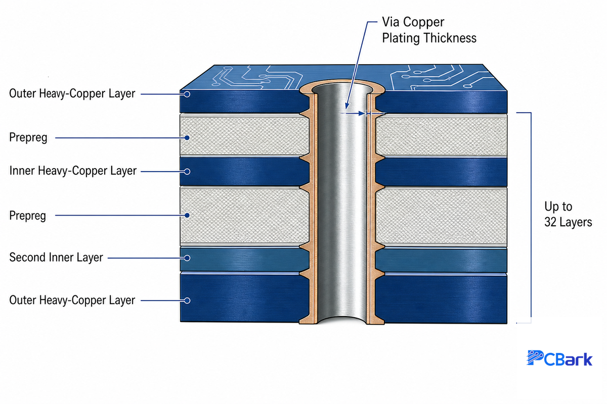
Heavy copper doesn’t restrict itself to external layers. When your design needs high current distributed to inner-layer power planes, common for multilayer power-electronics boards, the inner-layer copper weight and via design are much more significant limitations than they would be on a standard-copper multilayer stack-up.
Perhaps the most important limiting factor is the aspect ratio of the via hole (depth divided by width). Typically, manufacturers recommend a maximum aspect ratio of 6:1 for heavy-copper vias and 4:1 if the vias is carrying high current or used for thermal purposes because uniform copper plating along the via hole’s inner wall is hard to achieve in very deep/narrow holes. The full ipc-2152 standard even contains a detailed appendix for via temperature gradients, which is worth reviewing in such cases, rather than depending on a single maximum aspect-ratio value. Getting the aspect ratio wrong is a common and expensive mistake: a via drilled too deep and too narrow for its plating process risks incomplete copper coverage on the barrel wall, a defect that often escapes visual inspection and only shows up as an intermittent connection failure in the field within 90 days, because standard drilling parameters were never built around holes this deep relative to their diameter.
On multilayer heavy-copper PCBs, the construction method called “copper-filled vias” (sometimes “via-in-pad” construction) is often employed under high-power components and BGA packages. These fill-ins not only help the component to efficiently conduct heat through the entire PCB stack-up but also provide a flat, solderable pad to the above component, with copper plating extending down the via sidewalls to keep the thermal path conductive from top to bottom. Planning the stack-up must also account for balancing copper thickness on either side of the stack. Unequal thickness on opposite sides (i.e., heavy copper on one side, thin copper on the other) causes unequal stress on the laminate during board manufacturing, potentially leading to warpage, so heavy-copper designs are typically built to balance copper thicknesses on each layer before finalizing the stack-up, even if not explicitly done for electrical- performance alone. Dedicating separate heavy-copper planes to power and ground, rather than mixing them with fine-pitch control circuits on the same layer, is a design and fabrication decision worth making early rather than after the stack-up is locked. PCBark’s multilayer PCB capability automatically includes planning for heavy copper on inner layers, not as an exceptional process.
Standards, Acceptance Classes & Reliability Testing
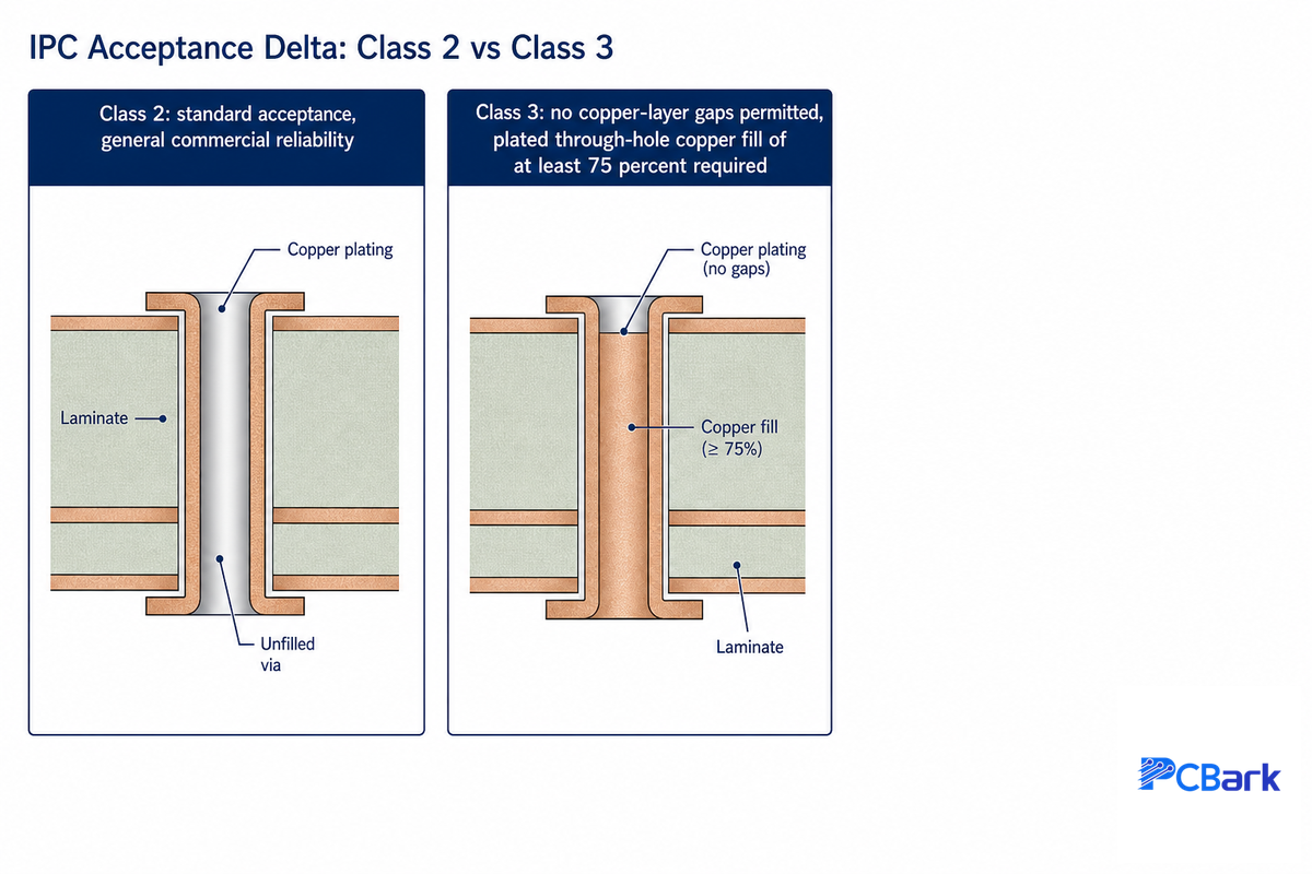
The acceptance of a heavy copper board is covered by two different standards: IPC-6012 for a performance specification of a printed board and IPC-A-600 for the acceptability of the visual quality of the bare printed boards such as annular ring, plating thickness and holes quality, while the IPC-A-610 defines acceptability criteria for the electronic assembly such as solder connections and their associated workmanship standards. Most PCB fabricators cite a Class 2/3 certification against the IPC-A-610, as it describes the requirements for the electronic assembly step of a finished product, whereas the bare board acceptance is defined under the IPC-6012. Our certifications include IPC-A-610 Class 2 and 3 for workmanship, as well as ISO 9001 and ISO 14001 certifications for quality and environmental management, plus a UL certification and RoHS/REACH compliance for product safety and regulatory compliance. Class 3 refers to the higher reliability acceptance level generally recommended for applications such as defense, aerospace, and medical devices where even minor defects may be critical — the same high-reliability bar documented in IEEE research on PWB conductor reliability in demanding (space-qualified) environments.
Although the acceptance class refers to the acceptable look of the final printed board, reliability testing provides data to determine if the final printed board will survive the intended environment over its service life. The relevant standard for this purpose is the IPC-9701 which provides guidance on the thermal cycling testing of solder attachments for fatigue life prediction of surface mount devices (SMD). Heavy copper is affected disproportionately due to the Coefficient of Thermal Expansion (CTE) difference between the copper foil and the substrate material. As a heavy copper board under goes temperature cycles between the two extreme temperature values, copper foil and laminate expand and contract at different rates, concentrating stress at the vias, causing the crack propagation until electrical resistance is impacted significantly. A test reported by one PCB manufacturer demonstrated that an FR-4 board with thin copper (0.8-1.2 mils thick) experienced a 32% crack failure rate after 8 thermal cycles whereas an identical board with heavy copper (2 oz / 2.5 mil) failed with a 0.57% crack rate under the same conditions – approximately a 50-fold increase due to heavy copper plating in this particular case. It should be noted that the 0.57% crack failure rate is based on a single manufacturer’s test results and not an independent, audited study.
Applications: The Engineering Logic Behind Each Use Case

Most heavy copper applications list industries like automotive, aerospace, and renewable energy as key segments without detailing what particular failure mechanism heavy copper prevents within these industries. Heavy copper PCBs are used wherever a design that would otherwise need a simple board with a bolted-on busbar has to carry higher current in a smaller footprint, and the copper weight is used in power electronics specifically to move that current without a separate bus bar. A table below summarizes some of these common use cases, matching the relevant failure mechanism to the copper weight choice and grouping “power electronics” by specific application failure modes rather than a general classification.
| Application | Dominant Failure Mode | Typical Copper Range |
|---|---|---|
| EV traction inverters & onboard chargers | Continuous high current + thermal cycling under drive-cycle load swings | 4-10 oz outer, plated heat vias |
| Industrial power supplies & motor drives | I²R resistive heating at sustained rated load | 3-6 oz outer/inner |
| Renewable inverters & battery management busbars | High continuous current density across wide copper planes | 6-20 oz, on-board plated busbars |
| Military/aerospace power distribution & radar power | Combined thermal, mechanical shock, and vibration robustness | 4-20 oz, mil-spec laminates |
Particularly the EV and renewable energy cases are where published case data exist, but the same caution as with any single manufacturer’s self-reported numbers should apply: A PCB manufacturer case study shows an EV charger power module of 400 A re-engineered from 2oz to 6oz copper, reducing board size by 35% and eliminating external heatsinks; A different case study by the same manufacturer shows a solar inverter design moving from 1oz to 4oz copper on outer layers reducing layer count from 12 to 8, improving the MTBF from about 85k to 240k hours. In both cases the figures are from vendor published case studies, not from an independent verified test report, and were included solely to indicate the scope of discussion about design that heavy copper enable, not as assured results. Where a design profile falls into one of the descriptions above, PCBark’s heavy copper PCB manufacturing capability (2-20 oz outer, 2-12 oz inner, up to 32 layers) provides coverage of the full table range on a production basis, not just prototype service.
Common Design Mistakes Engineers Make
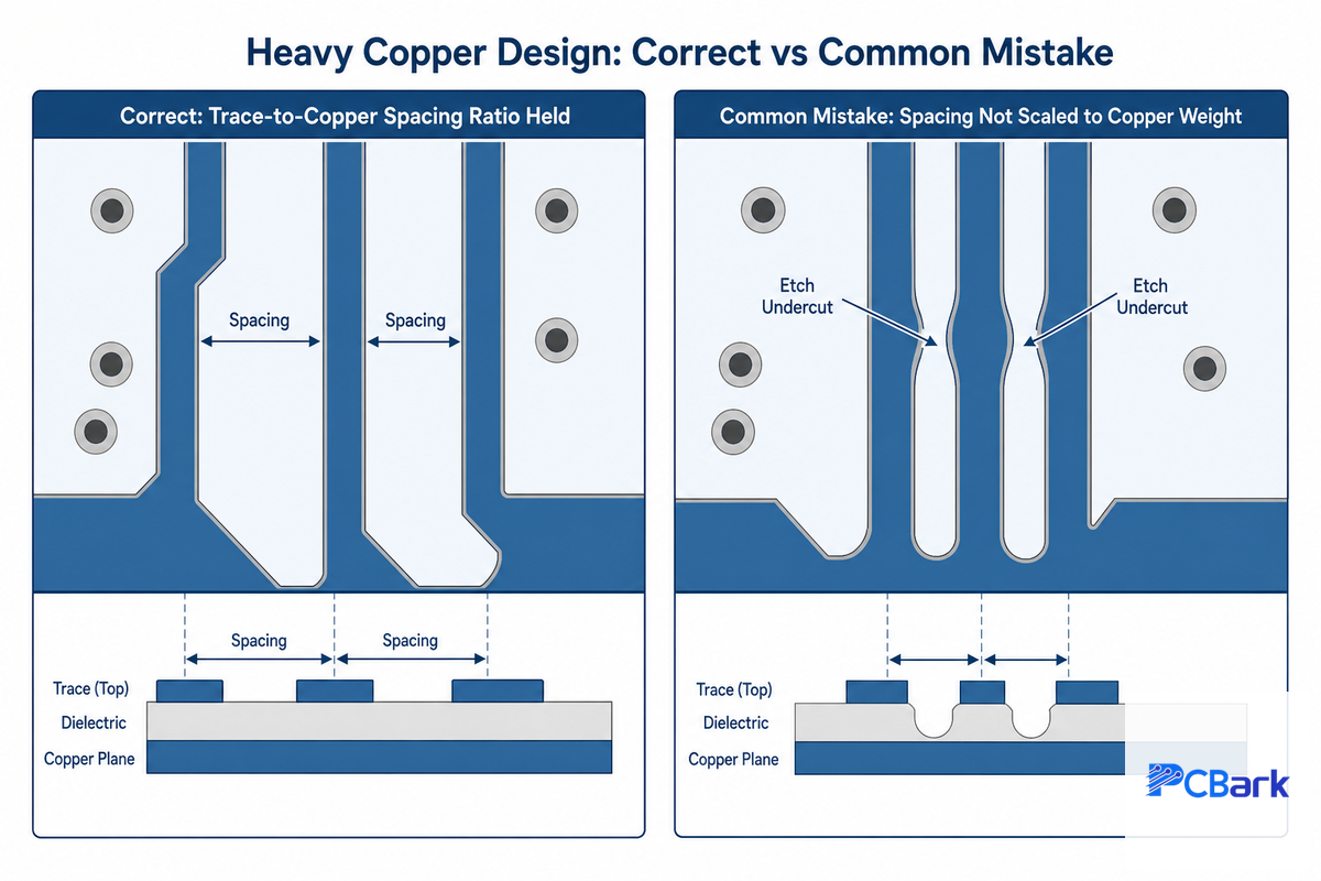
A relatively consistent pattern of design-file problems have been observed by fabricators with heavy copper jobs. most of which come from the reuse of standard copper design rules on a heavy copper layout rather than modification to accommodate the thick copper.
- Insufficient trace/space minima, usually from reuse of standard copper design rules, where a standard minimum of, say, 6 mil trace/space, becomes too small on a thick board: on 3oz boards it’s usually 10 mil, and for 6oz boards often 16 to 20 mil minimum, because etching tolerances grow as copper thickens.
- Poor copper balance through out the stack up – a common reason fabricators report warpage during lamination for multi layer heavy copper boards. See section H2-6 on warpage.
- Lack of adequate thermal relief for pad spoke connection to thick planes, leading to a failure to properly reflow solder and resulting in cold joints in assembly.
- Overly ambitious via aspect ratio that exceed the H2-6 recommendation of 6:1 resulting in voiding that may only be detectable in cross section inspection.
- The possibility of de-lamination and resin voiding increase as copper thickness and inner-layer misalignment increase, especially on thin core substrates; a potential failure issue fabricators explicitly note for multi layer heavy copper boards (not for standard copper).
There’s a simple solution to all of these issues: Submit layer stack up, layer weight, and target thermal rise information to your manufacturer before the design is locked. Each of the design rules mentioned above is different depending on the particular number of layers and copper weight, precisely the kind of problem a design-for-manufacturability review on a drawing can prevent at a cross sectioned failed board. PCBark’s DFM analysis process checks layer stackup copper balance, and via aspect ratio against those exact failure conditions before a heavy copper design proceeds to manufacturing.
Industry Outlook

But the driver of increased heavy copper use isn’t search-volume trends – Search data from DataForSEO on the core “heavy copper pcb” keywords remains flat to down slightly on an annual basis, typical for a mature, specialized engineering topic and not an indication of declining interest. Current density is the driver; current density is up for EV traction inverters, onboard chargers and grid-scale renewable energy sources power electronics and more continuous current per board footprint, a higher standard than power-electronics designers considered five years ago. It’s an engineering requirement shift, not a marketing one, and you see that in related standards activity -IPC-2221 (the standard that includes the base current capacity charts that many engineers will still consult first) was most recently updated in December 2023, and IPC-9701’s thermal cycling test method in February 2022, showing the groups that define the standards in this space actively respond to high power, high reliability designs, not treating the established method as set in stone. Academic research is moving the same direction — IEEE-published trace current-capacity research continues to refine the models this industry activity is built on.
From a process standpoint, at least one manufacturer in this space has forecast that the next evolution of heavy copper will include ultra heavy-copper (>10-20oz) alongside metal-core or thermal coin embedded construction, with additive processes selectively building up copper only where it’s needed, rather than uniformly over an entire layer. That forecast warrants watching, but it isn’t an industry standard today. Several market research firms separately estimate the global heavy-copper pcb market growing at somewhere between approximately 8% and 14% per year, so that number is probably best taken as directional. If a designer is looking at an application today with a similar-sized board footprint that will require more continuous current in 2026 than it does today, then it’s worth evaluating heavy copper for that design at the concept level and not at the post-design phase. The risk of ignoring that shift is real: sticking with a 2 oz layout for a design that now needs to carry 40% more current risks a board that runs hot in the field within 1 year, because the copper mass was built around yesterday’s power budget, not today’s. PCBark has adjusted its own in-house production planning around exactly this shift over 16 years of production in the industry.
Frequently Asked Questions
Q: What is the maximum copper thickness available for a PCB?
View Answer
Heavy copper is available from fabricators on a standard-production basis up to 20 oz/ft² (roughly 700 µm, or 27.4 mil), which is the range covered in this article. Extremely-heavy copper, beyond this, is available up to 200 oz/ft² in special applications such as plated onboard heat sinks or planar transformers from a few specialized manufacturers. Availability, though, diminishes considerably beyond about 30-40 oz because few fabricators offer such high-copper densities regularly.
Q: How is heavy copper PCB pricing different from a standard PCB?
View Answer
Heavy copper isn’t expensive for one single reason, though it grows exponentially with higher copper weight due to the compounding of several effects: raw copper cost goes up linearly with extra copper, the etching and plating process time is increased because more copper has to be removed and/or deposited, and yields tend to drop at heavy weights because the process tolerances are much tighter. Some recent discussion within the community suggests that doubling copper weight from 1oz to 2oz adds perhaps 20-40% to the etch and raw material cost, and that cost factor tends to continue to rise on 4oz, 6oz, etc. This depends strongly on panel usage and the particular manufacturer’s capabilities, of course.
Q: What is the 3W rule in PCB design?
View Answer
The 3W rule is a trace separation rule that states that the space between two parallel traces must be equal to at least three times the trace width, in order to limit the electromagnetic interference (EMI) and crosstalk between them. It is much more significant in heavy copper PCBs because the required separation for wider traces takes up a lot more real estate than would be the case on thinner 1oz copper traces, and that is why a layout often requires more room to route in heavy copper to carry a given amount of current.
Q: Can heavy copper PCBs be made as flex or rigid-flex boards?
View Answer
Yes, though to a lesser extent than rigid PCBs since heavy copper in a flex section can crack if flexed repeatedly. Most heavy copper flex and rigid-flex designs do not exceed 4oz copper weight in the areas where flexing occurs, saving it for rigid portions.
Q: What is copper pour in PCB design, and does it matter for heavy copper boards?
View Answer
A copper pour is an area of a layer filled with a large copper plane, as opposed to leaving the area bare substrate. This is done for reasons other than merely to occupy unused space on a heavy copper PCB, and carries more weight than for standard 1oz PCBs because of two primary factors: It affects the copper balance (as described in H2-6) to provide more uniform pressure and less board warp, and heavy copper acts as an excellent heat spreader, dissipating heat away from high temperature components into cooler areas of the PCB.
Q: Why does heavy copper cost more to fabricate than a standard board?
View Answer
Because additional process time and complexity is added on top of just material cost. Conventional etching processes begin to lose reliability beyond about 3oz and the manufacturer must use much slower, more complex differential etching and plating methods which demand much finer process control, lower yields per panel, and of course, extra copper. This explains why costs do not rise in direct proportion to copper weight.
Ready to Spec a Heavy Copper Build?
PCBark fabricates heavy copper pcbs in everything from 2 oz to 20 oz outer layer copper, 6mm board thickness, 32 layers and more, with IPC-A-610 Class 2 and 3 certified assembly. Send in your stack-up and current needs for a DFM analysis before committing to a copper weight.
Why We Write This
This document provides engineers a single source for making heavy copper pcb design choices-material, IPC-2152 versus IPC-2221 standards, accepted levels, and testing methods-as opposed to scattered over a dozen specialized single-topic pages found in many fabricator knowledge bases. This document references a single copper weight table and worked example of current-capacity calculation that relies on PCBark’s internal heavy-copper planning for fabrication capability (2 to 20 oz outer layer, 2 to 12 oz inner layer, and 32 layers). The goal throughout is maximum reliability for the PCB assembly step that follows fabrication, not just a passing fabrication inspection. Reviewed by PCBark (Shenzhen Linghangda Technology Co., Ltd.) technical team.
References & Sources
- On Current Carrying Capacities of PCB TracesIEEE Xplore
- Current-Carrying Capacity of PWB Internal Conductors in Space EnvironmentsIEEE Xplore
- IPC Standards Revision TableGlobal Electronics Association (IPC)
- IPC-2152, Current Carrying Capacity in Printed Board DesignAmerican National Standards Institute (ANSI)
- IPC-2152, Standard for Determining Current-Carrying Capacity in Printed Board DesignCircuit World, Emerald Publishing
- CN105163523A, Super-Thick Copper Etching Technique for PCBGoogle Patents
Related Articles
- Heavy Copper PCB Manufacturer, Capability & RFQthe commercial capability page for spec’ing and quoting a heavy copper build
- Multilayer PCB Manufacturingstack-up planning for heavy-copper multilayer boards
- Certifications & StandardsISO 9001, IPC-A-610 Class 2/3, UL, RoHS/REACH detail
- DFM Analysishow stack-up and copper-balance review works before fabrication
- Ceramic PCB Manufactureran alternative high-thermal-conductivity substrate for extreme thermal applications
- About PCBark16+ years of EMS manufacturing, 500,000 m² annual capacity