Get in touch with PCBark Company

Cost Pressure vs Quality Risk: The PCB Sourcing Trade-Off Every Buyer Faces
Pricing Two Risks at Once
Every PCB manufacturing quote forces a buyer to price two risks at once. Skew toward the cheapest board house and you risk batch-to-batch variation, fake or substituted parts on the assembly side, and QC escapes that only surface in the field. Skew toward a domestic premium shop and you pay two-to-three times more and often wait longer. One engineer put the dilemma plainly:
“I’ve been buying PCBs from Chinese companies for years and am very happy with the turn-around and quality, I’d just love a US-based option that isn’t absurdly expensive.”
The Root Cause of Regret
That tension is the real job of a printed circuit board manufacturer: not to be the cheapest line item, but to remove the variables that make cheap boards expensive later. The root cause of most “cheap board” regret isn’t the fabricator’s price, it’s the absence of a published, verifiable capability and build class, so the buyer can’t tell a 0.8 mil plating Class 2 board from a void-free Class 3 board until something fails, a reliability gap documented in published patent and standards literature.
The PCBark Standard
PCBark closes that gap by publishing the spec matrix, the IPC class rules, and the cost logic up front, then backing each board with AOI, X-ray, and electrical test. The result you get is a circuit board manufacturing decision you can defend to your own quality team, which is where the rest of this page is aimed.
// SYS.OP. NORMAL
PCB Substrate Types We Fabricate
The wrong substrate is one of the most expensive PCB manufacturing mistakes, an LED driver on standard FR-4 runs hot and fails early, while an RF front-end on the wrong dielectric drifts off-frequency.
Material choice is a thermal and electrical decision before it's a cost decision, so we fabricate the full specialty spectrum in-house rather than brokering it out.
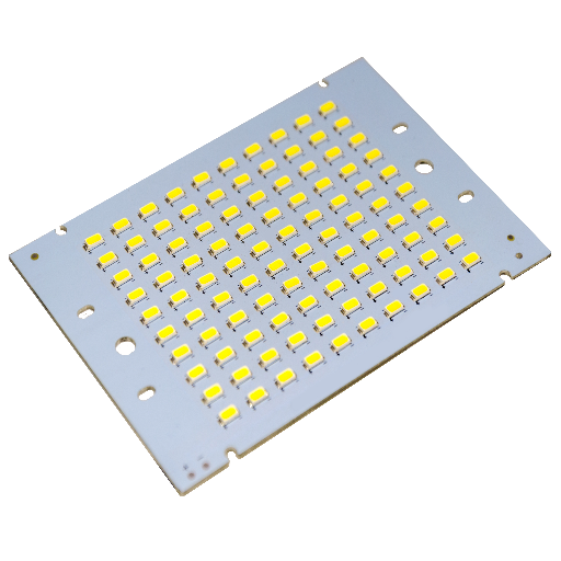
Aluminum / Metal Core (MCPCB)
Thermal conductivity for LED & power; single/double-layer MCPCB.
Aluminum PCB →
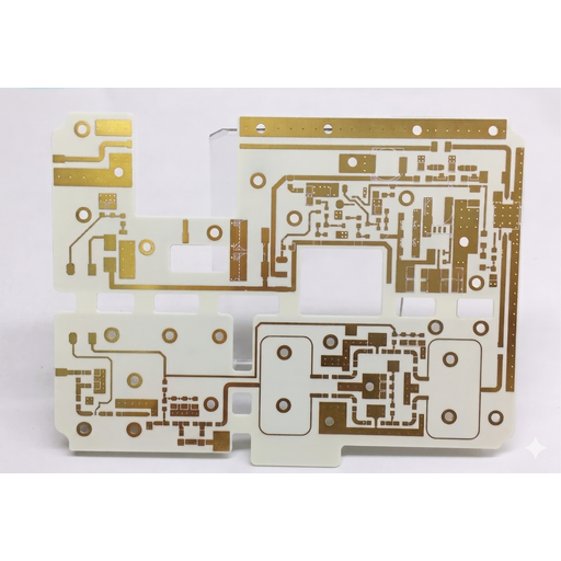
Ceramic PCB
Alumina & aluminum-nitride for high-temperature, high-reliability.
Ceramic PCB →
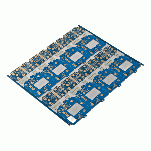
Rogers PCB / RF Substrate
RO4350B / RO4003C laminates for low-loss RF & microwave.
Rogers PCB →
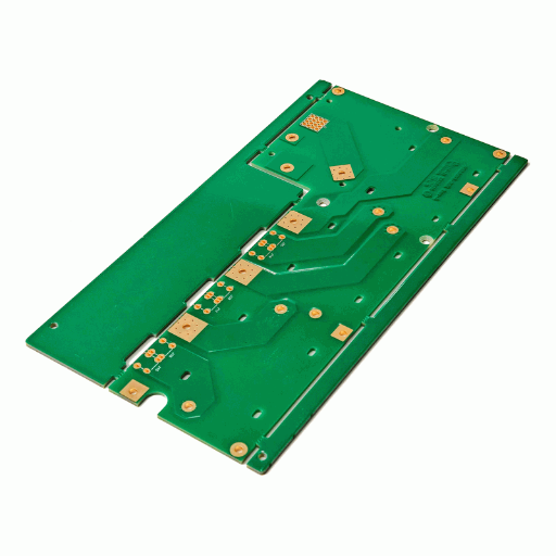
Heavy Copper PCB
Up to 8 oz copper for high-current power distribution.
Heavy Copper PCB →
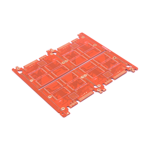
Gold Finger PCB
Hard-gold plated edge connectors for high-cycle insertion.
Gold Finger PCB →
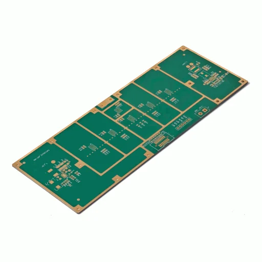
High Frequency / RF / Microwave PCB
Controlled-Dk laminates for antenna, radar & high-speed digital.
High Frequency PCB →
The 6-Substrate Material Selection Spectrum
| Substrate | Drives | Typical use |
|---|---|---|
| FR-4 (Tg 130–170) | Cost / general purpose | Consumer, control, IoT |
| Aluminum / Metal Core | Heat dissipation | LED, power converters |
| Ceramic (Alumina / AlN) | Thermal + RF stability | Power electronics, sensors |
| Rogers (RO4350B/RO4003C) | Low dielectric loss | RF, microwave, 5G |
| Heavy Copper (to 8 oz) | Current / thermal mass | Power distribution, automotive |
| High-Frequency / RF | Signal integrity | Antennas, radar, high-speed digital |
These specialty substrates feed multilayer, HDI and rigid-flex builds on the same lines, for layer-count detail see our multilayer PCB and HDI PCB capabilities. How those materials are imaged, drilled, plated and verified is the process question we answer next.
From Gerber to Shipped Board, Our Fabrication & Test Process
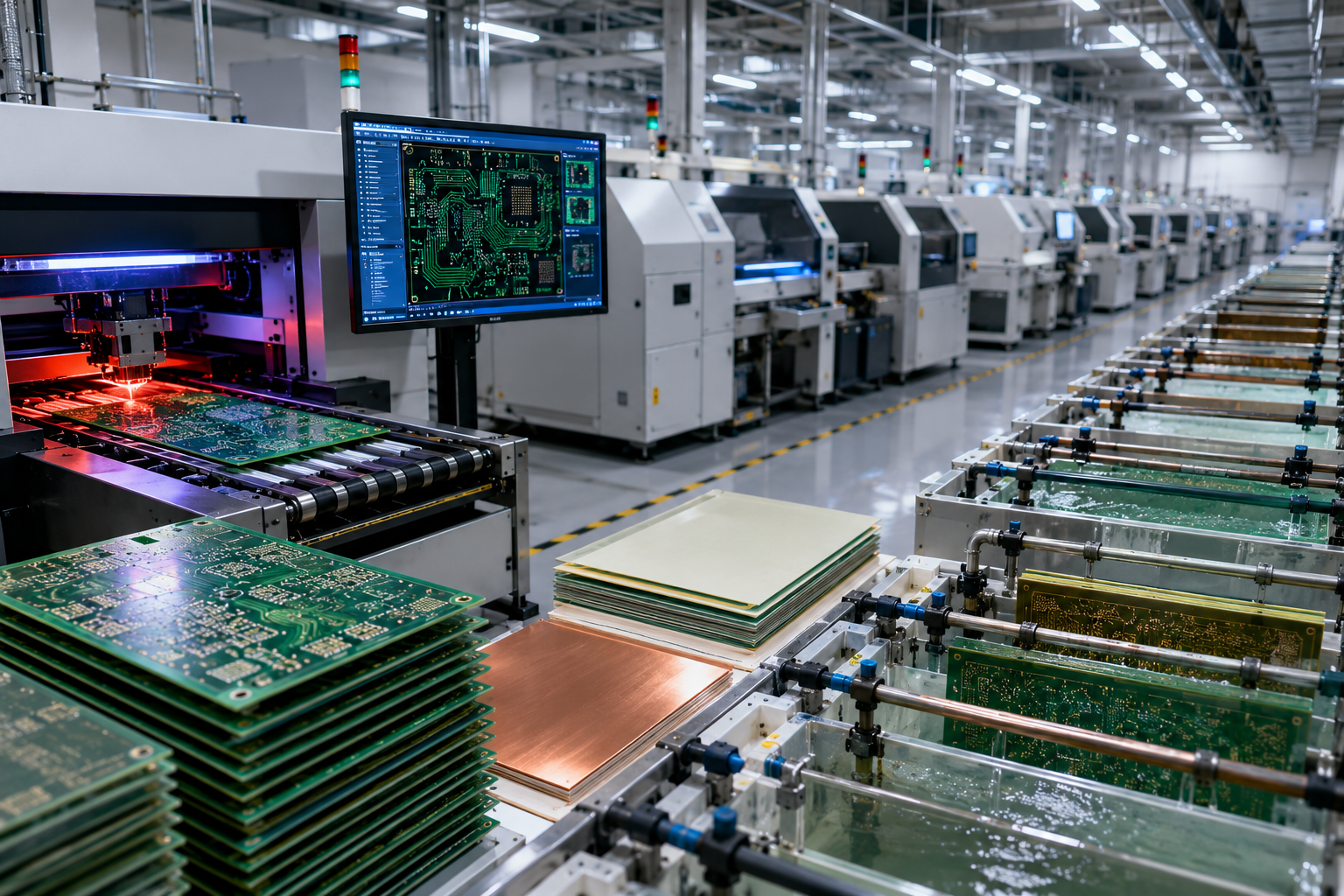
A clean-looking board doesn't always guarantee long-term reliability, if plated-hole copper is too thin it can pass a visual check and still fail under thermal cycling. That's why PCB manufacturing reliability is decided at the process and test stages, not at final inspection of cosmetics. Our flow is built so each board is verified against the capability index above before it leaves the line.
01
Fabrication flow
It starts with your PCB design and Gerber files: front-end CAM and DFM → inner-layer imaging and etch → lamination → CNC mechanical and laser drilling → electroless and electrolytic copper plating → outer-layer image/etch → solder mask and silkscreen → surface finish → CNC profiling and electrical test. The expensive mistake is treating plating as a commodity step: PCBark's process engineers gate every panel at the plating bath because a 25 µm (1 mil) Class 3 hole wall can't be recovered after lamination, it has to be built in, not inspected in.
Surface preparation matters more than buyers expect: published patent literature describes polymer-bonding pretreatment to remove copper-surface oxidation without aggressive micro-etch (e.g., TW 2024-02120A), and plasma semi-additive processing (CN 101102647B) for fine-line density, the same class of techniques that make 3 mil traces and high-layer-count builds repeatable in production, not just in a one-off prototype.
02
Test & inspection stack
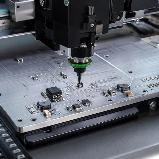
Every PCBA order runs through AOI (automated optical inspection), 3D X-ray for BGA and hidden joints, ICT and Flying Probe electrical test, burn-in, and functional test; bare boards receive electrical (E-test) verification. This is the layer that catches the failure mode buyers actually report from budget fabs, missing inner layers, cold joints, and substituted parts, before boards ship, not after they brick in the field.
A documented process is only worth what an independent standard says it is, which is why build class and certification, covered two sections down, aren't a logo wall but an acceptance contract. First, the cost question every buyer leads with. For drilling and plating reliability references, see acceptance criteria published via patent literature on embedded-copper thermal designs.
Want your stackup checked against our 3 mil trace and 25 µm plating limits before you commit?
China Cost Without the China Risk, Landed-Cost & Quality Crosswalk
Is China always cheaper for PCB manufacturing? Not always. That is the starting point of a real sourcing decision. The sticker price is only one input; the number that actually hits your budget is the landed cost, unit price plus duty, freight, and the cost of any quality escape. Buyers who skip that math get surprised at customs; buyers who run it usually find the answer is still favorable, but for reasons they can defend.
The China-vs-US PCB Landed-Cost Crosswalk
US import duty on printed circuit boards (HS heading 8534.00.00) is significant and changes often. As of June 23, 2026, updated industry tariff monitors report rates running roughly 30% on double-sided and 4-layer rigid boards and up to 55% on single-sided, multilayer, and flexible boards, with Section 301 measures on Chinese imports ongoing and exclusions lapsed. The practical implication: you must calculate duty by board type, not assume a flat number.
| Landed-cost factor | What to check | How PCBark de-risks it |
|---|---|---|
| Unit price | Quote for your exact stackup | Transparent spec-based quote, no maker promo |
| Import duty | HS 8534 rate by board type (30–55%) | We flag the applicable category up front |
| Freight + lead time | Air vs sea; expedite cost | Quick-turn options keep total time competitive |
| Quality-escape cost | Rework, field failure, recall | Class 2/3 build + full test stack reduces escapes |
3×
Buyers routinely report China-fabricated boards landing at roughly one-third the cost of a comparable US order — even after shipping — when the board is spec-matched and the duty category is known.
FIG. 01 / CROSSWALK DATA

Cost only stays an advantage if quality holds, and quality, in PCB manufacturing, is defined by an inspectable build class rather than a marketing adjective. That's the next section. (Authoritative duty references: U.S. Customs and Border Protection.)
×
Quality, Certifications & Build Tiers, IPC Class 2 vs Class 3
The one genuine hesitation buyers raise about offshore PCB manufacturing is trust on regulated boards, even those who say "the quality is always good" still ask how to prove it. The answer isn't a brand name; it's a build class your auditor can check. The most common buyer error is specifying the wrong class, paying Class 3 prices for a Class 2 product, or worse, shipping a Class 2 board into a medical or automotive application that demanded Class 3.
The IPC Class 2 vs Class 3 Build-Tier Selector
The difference is concrete and measurable, not a subjective label. Per published IPC design-rule references, the key distinction is annular-ring and plated-hole integrity:
| Criterion | Class 2 (dedicated service) | Class 3 (high-reliability) |
|---|---|---|
| Internal annular ring | Relaxed (breakout allowed) | ≥ 1 mil, near-perfect registration |
| External annular ring | Relaxed | ≥ 2 mil |
| Plated-hole voids | 1 void allowed in 5% of holes | No voids permitted |
| Copper plating thickness | 0.8 mil | 1.0 mil (25 µm) |
| Best for | Consumer, industrial control | Medical, auto, aerospace, defense |
PCBark fabricates to both classes and inspects to IPC-A-610 Class 2/3 with J-STD-001 soldering, so when your application demands the void-free plating and 25 µm hole-wall copper of Class 3, the board is built and documented to that contract.
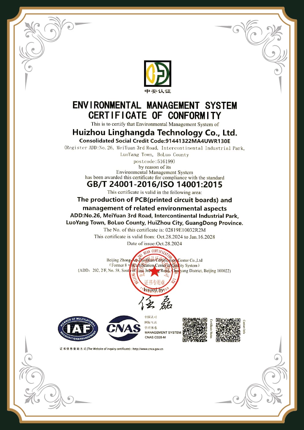
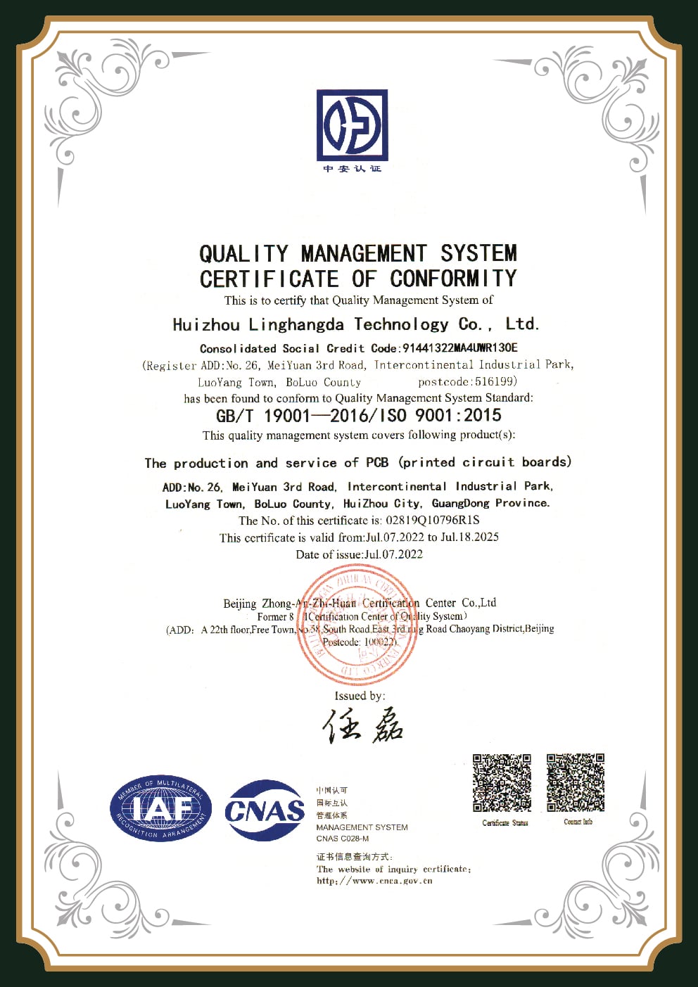
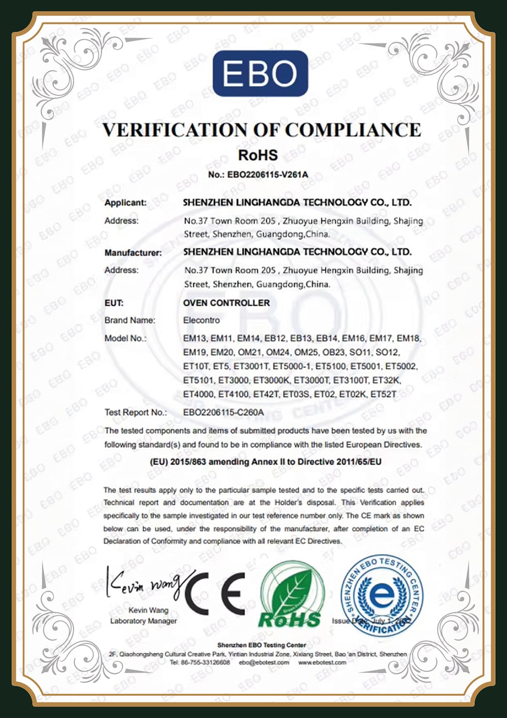
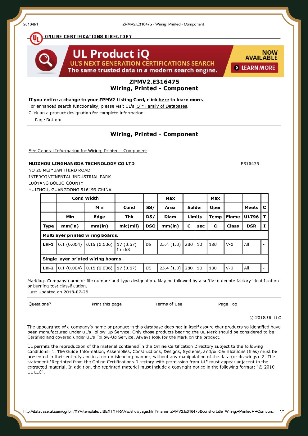
Certification Stack
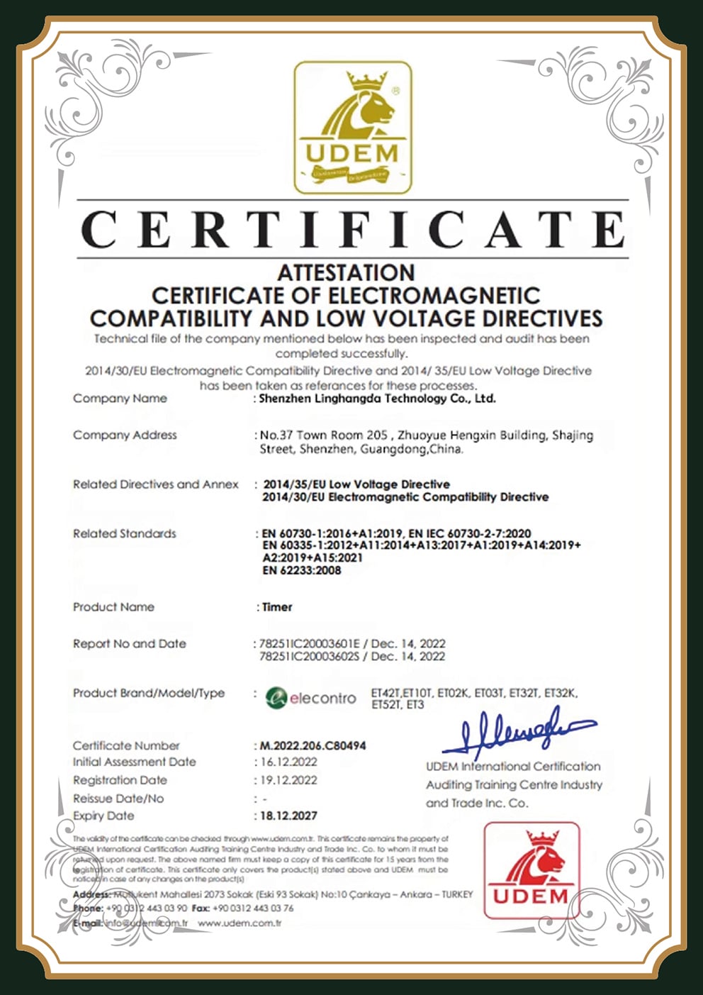
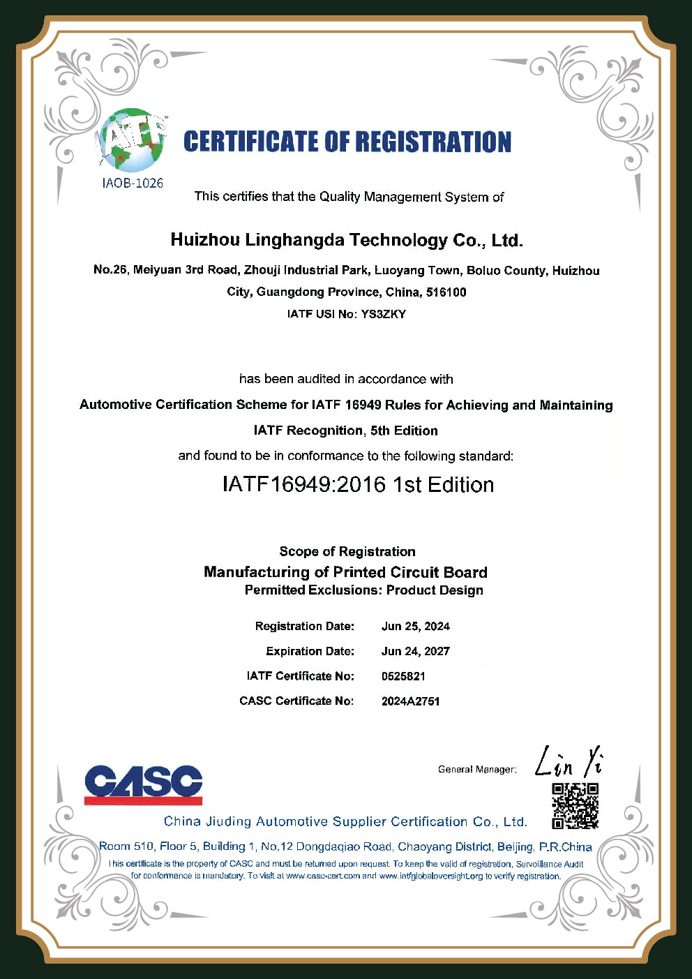
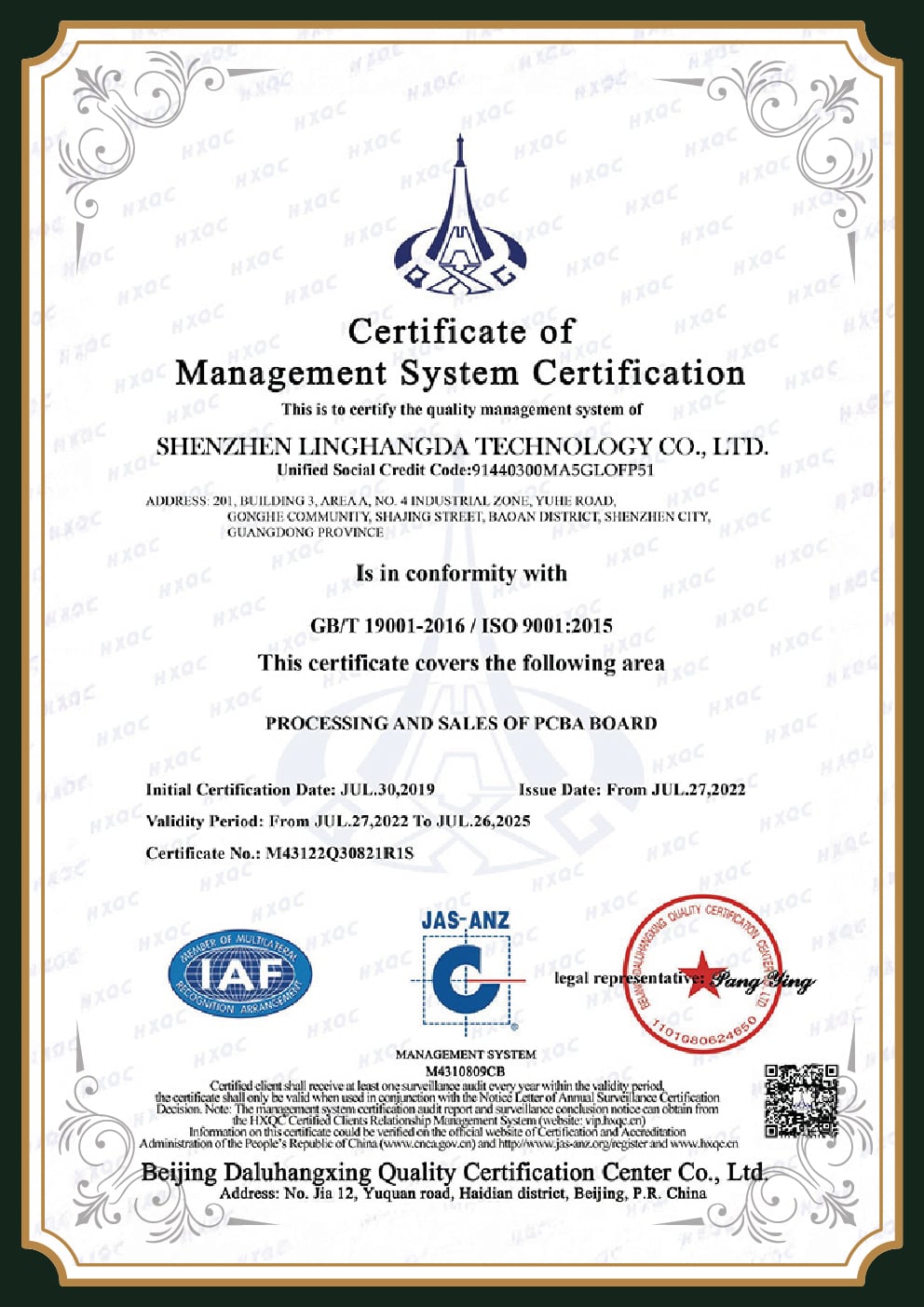
ISO 9001:2015Quality mgmt
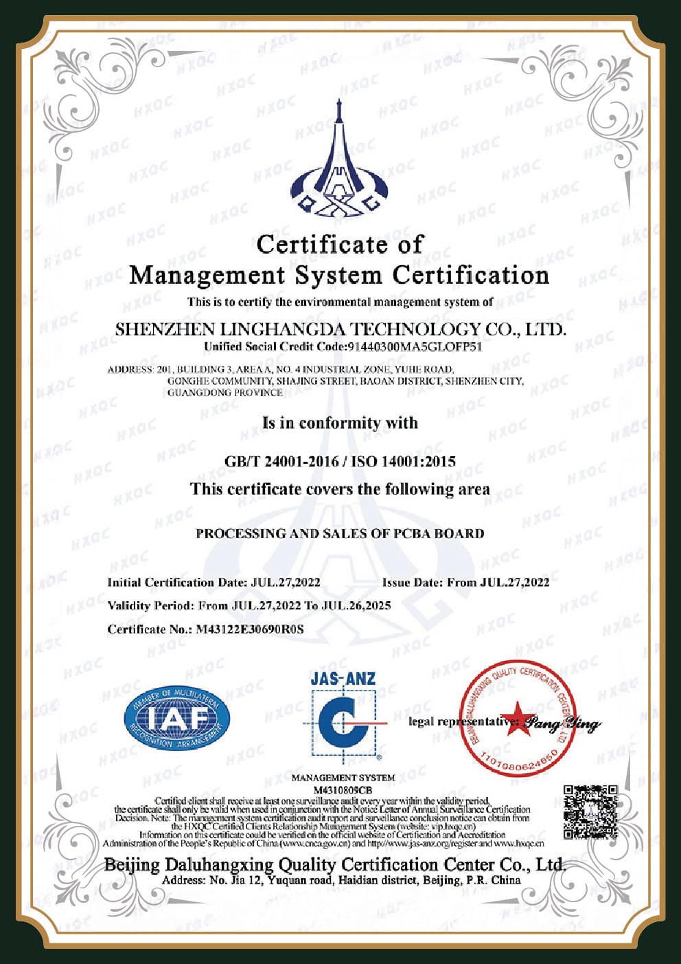
ISO 14001Environmental
IATF 16949Automotive
ULListed
RoHS / REACHCompliance
IPC-A-610 2/3+ J-STD-001
That certification stack, shown below, including IATF 16949, is what lets buyers route automotive and high-reliability work to PCBark rather than a maker-grade portal. Standards references: ISO 9001:2015.
Industries We Serve
Specifying the wrong board class for a regulated industry is an expensive mistake, a Class 2 board dropped into a medical or automotive application can pass a visual check and still fail field reliability, triggering recalls that dwarf the board cost. PCBark fabricates for consumer electronics, medical devices, automotive and EV electronics, industrial control, robotics, IoT, aerospace and drones, the same application mix that drove our certification choices.
The reason those certifications matter is contractual, not cosmetic: PCBark builds automotive boards under IATF 16949 in-house and defaults medical, aerospace, and defense work to the void-free Class 3 plating tier (25 µm hole wall), because those sectors can't accept the single-void-in-5%-of-holes tolerance that Class 2 permits. Application-specific stackups, aluminum for LED thermal loads, Rogers for RF, heavy copper for power distribution, map to the substrate spectrum on the same production lines, which keeps qualification consistent across your product portfolio. For sector reliability context, see NIST electronics reliability references.
1 / 4
Procurement Guide, Lead Times, MOQ, Quoting & Full Turnkey
[ ROLE: PROCUREMENT & MGMT ]
Two procurement risks sink more PCB orders than price: slow lead times and vendor finger-pointing when the fab and the assembler are different companies. Buyers consistently report China turnaround "in under a week" even with shipping; the harder problem is accountability when something goes wrong mid-build.
Professional PCB Engineering & Estimation Tools
PCB Manufacturing Cost Estimator
A directional estimate from PCBark’s real fabrication capability. Final quote depends on your Gerber files — this tool shows the drivers.
Access Estimator
China-vs-US PCB Landed-Cost Calculator
Sticker price is not landed cost. Add HS 8534 import duty + freight to see the real comparison — honestly.
Calculate Landed Cost
IPC Class 2 vs Class 3 Build-Tier Selector
Specifying the wrong class wastes money (Class 3 you didn’t need) or risks field failure (Class 2 where you needed 3). Answer 5 questions.
Launch Selector
PCB fabrication (manufacturing) produces the bare printed circuit board, the laminate, copper layers, drilling, plating, solder mask, and surface finish. PCB assembly (PCBA) then mounts and solders components onto that bare board. PCBark does both under one roof, so a single factory is accountable from Gerber to a tested, populated board.
Yes. IPC Class 3 is a measurable build standard, internal annular ring ≥ 1 mil, external ≥ 2 mil, no plated-hole voids, and 1.0 mil (25 µm) hole-wall copper. PCBark fabricates to Class 3 and inspects to IPC-A-610 Class 2/3 with J-STD-001 soldering, with a full inspection record you can present to a quality auditor.
US import duty on PCBs (HS 8534.00.00) currently ranges from about 30% on double-sided and 4-layer rigid boards to 55% on single-sided, multilayer, and flexible boards, and Section 301 measures are ongoing. The right approach is to calculate landed cost = unit price + duty (by board type) + freight, not assume a flat figure. Even after duty, buyers commonly report a meaningful total-cost advantage. We flag your duty category in the quote so there are no customs surprises.
Up to 42 layers. Standard production runs 1–20 layers; 22–42 layer builds support high-density backplanes and complex RF stacks. This is wider than the 30–32 layer ceiling most prototype-focused competitors publish.
We offer HASL (lead-free), OSP, ENIG, ENEPIG, immersion silver, immersion tin, and hard gold. OSP is lowest cost for quick-turn; ENIG suits fine-pitch and flat-pad requirements; hard gold is for edge connectors (gold fingers). We recommend a finish during DFM based on your pitch, shelf life, and assembly method.
There is no MOQ for a PCB prototype. We fabricate from a single piece, and the same lines scale to high-volume production runs. This lets you build a custom PCB prototype and mass-produce it with one qualified supplier.
We're direct about this: ITAR registration requires US-based fabrication, so a China factory can't hold it. For ITAR-controlled designs, choose a US fab. For the much larger set of non-ITAR aerospace, defense, and high-reliability work, PCBark builds to the void-free IPC Class 3 tier with full documentation, and we'll tell you during DFM if your project genuinely needs ITAR-registered sourcing.
Yes. PCBark provides full turnkey: DFM review, bare-board fabrication, transparent component sourcing, SMT and through-hole assembly, and functional testing, all under one roof, with the factory as the single point of accountability and IP handled under NDA.
Send Gerber files (and a BOM plus pick-and-place file for assembly). Include layer count, board size, quantity, copper weight, surface finish, material, and build class if known, or request a free DFM review and we'll recommend them. You'll receive a transparent, itemized quote with the applicable duty category noted.
SYS.SECURE
Get a PCB Manufacturing Quote You Can Verify
Send your Gerber files for a transparent, itemized quote, with the layer count checked against our capability index and the duty category flagged before you commit.
EXECUTE QUOTEX:145.8 Y:92.4 // LAYER_CHK: OK