
Get in touch with PCBark Company


Quick Specs
| Substrate materials | Al₂O₃ (alumina), AlN, Si₃N₄, BeO |
| Thermal conductivity (bulk, room temp) | 24–320 W/m·K, material-dependent |
| Operating temperature | −55°C to 350°C+ (tier-dependent) |
| Dielectric constant | ~6.8–10 (material-dependent) |
| Metallization routes | Thick film, thin film, DPC, DBC, AMB, LTCC/HTCC |
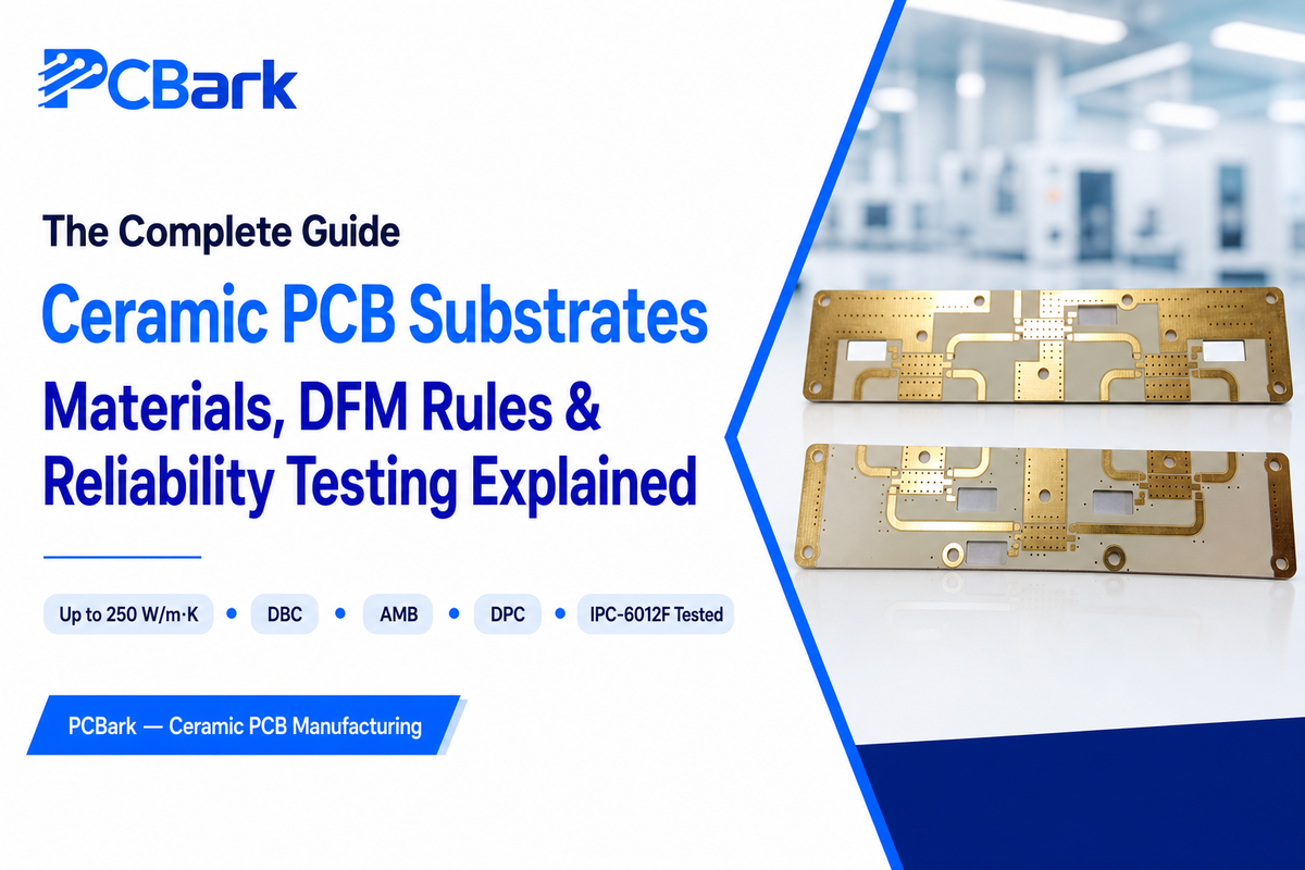
A ceramic PCB replaces an FR-4 board’s glass-reinforced epoxy with an inorganic ceramic substrate, alumina, aluminum nitride, silicon nitride, or beryllium oxide, so thermal and electrical stress is borne by an entirely different material system rather than a laminate stack. Engineers reach for these materials when a design’s thermal load, required voltage isolation, or operating-temperature range would take a board past FR-4’s limits, and high-performance power electronics increasingly depend on the high thermal conductivity these materials deliver. This guide cover the physics that make this substitution work, how each material and bonding process actually performs, how to design and verify a build around it, and where the technology is headed as wide-bandgap power semiconductors reshape demand. Buyers comparing ceramic PCB solutions against traditional PCBs built on standard PCB materials like FR4 are really asking how much this circuit board technology’s added cost buys in reliability, and traditional PCBs remain the right call whenever that added cost buys nothing a design actually needs.
Heat is transmitted through a ceramic pcb substrate via its crystal lattice structure, rather than its polymer resin, delivering thermal conductivities 50 to more than 600 times higher than that of typical FR-4 (about 0.3-0.5 W/mK). This property difference is why these substrates turn up in power modules, RF amplifiers, and anything where a component under heat will bake whatever lies below it.
What Is a Ceramic PCB? Structure, Materials, and the Physics of Why It Beats FR-4
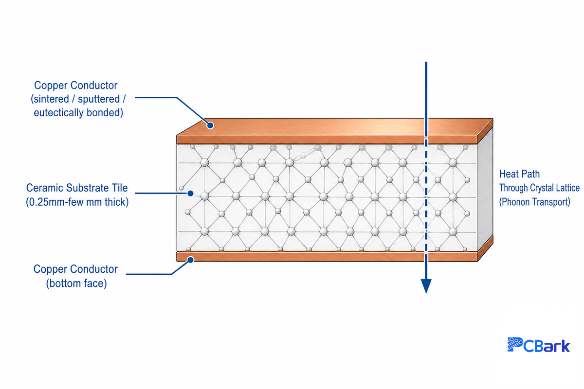
Fabrication of a ceramic PCB is a fundamentally different manufacturing process than etching a blank FR-4 panel. In terms of physical construction, a finished part is basically a solid flat chip, typically 0.25 mm to a few millimeters thick, with a copper circuit bonded to either side, sintered on (thick film), sputtered on (thin film), or thermally bonded at high temperature and pressure (DBC, AMB).
There’s no glass fiber weave and no epoxy binding layers together; this direct ceramic-to-copper connection, instead of a glass-laminate interface, is what eliminates the thermal resistance bottleneck an FR-4 PCB carries at that same junction. Thick film ceramic PCB construction is usually the most affordable option in this space, but producing true ceramic PCBs through the DBC/AMB route requires a specialized oven that most general-purpose board houses don’t have on hand. Ceramic PCB fabrication at every tier differs fundamentally from the tooling used for organic boards. The next sections cover the types of ceramic PCBs available and where each one truly shines.
Why this works boils down to how heat moves in each substance. With FR-4, the heat must traverse a polymer resin in which lengthy, jumbled molecular chains scatter the vibrational energy almost as fast as they can carry it – which is why FR-4 only has a conductivity around 0.3-0.5 W/mK. The crystalline structure of ceramic, on the other hand, is a better conduit for heat: heat moves as discrete units of lattice vibrations, or phonons, and within a regular crystal structure, phonons propagate long distances before scattering. This accounts for alumina’s conductivity of 24-30 W/mK and aluminum nitride’s still greater overall conductivity. This is an authentic difference in materials science rather than a marketing figure; a 2024 reliability study of PCB assemblies under thermal and vibration cycling found that thermal-path efficiency at the substrate level is one of the strongest predictors of long-term solder-joint survival, independent of the assembly’s design otherwise.
There’s another advantage these substrates offer that’s much less talked about: coefficient of thermal expansion (CTE) matching. Chip dies have an expansion/contraction of about 2.6 ppm/K. While aluminum nitride is pretty close (4.6 ppm/K) and silicon nitride even closer (2.5 ppm/K), the chip-to-substrate interface doesn’t experience as much stress due to the mismatched coefficients of expansion/contraction in each thermal cycle compared to organic materials. That’s also why ceramic is much more than just “a better heatsink”-it fundamentally alters the mechanical fatigue equation. Matched CTE plus a well-bonded interface is what turns a raw conductivity number into better heat dissipation at the point that actually matters, the die-attach line, which is exactly why thermal management engineers treat CTE matching as inseparable from raw conductivity when they spec a substrate.
When ceramic doesn’t make sense: if the design run cold, will ship in consumer quantities, and doesn’t require voltage isolation any greater than you already get from FR-4, the price tag and lead time associated with ceramic simply aren’t worth it. Engineers use ceramic when heat, voltage isolation, RF loss, or harsh-environment reliability becomes the actual design driver, not by default. If so, take a look at the PCBark ceramic pcb capability tiers to get an idea of what a build at each level will entail.
The Four Ceramic Substrate Materials, Compared by Where Each One Actually Wins
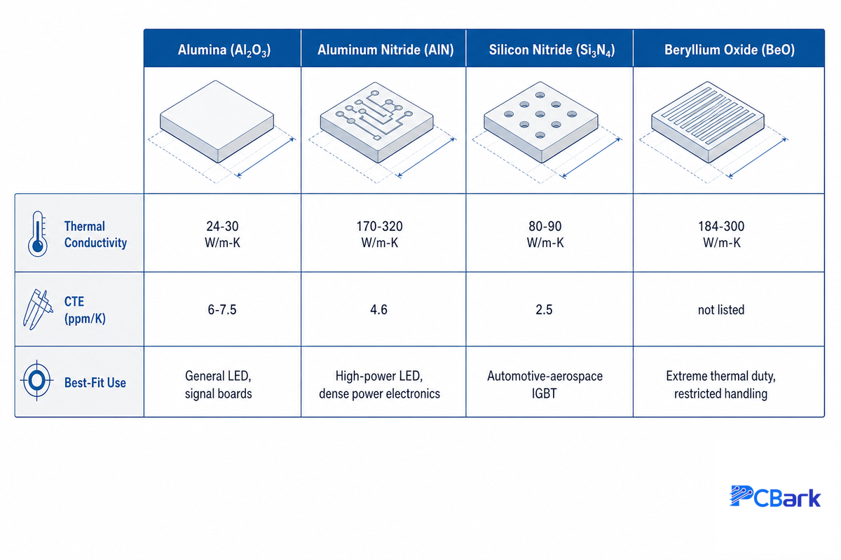
Four ceramics, alumina (aluminum oxide), aluminum nitride, silicon nitride, and beryllium oxide, show up repeatedly in PCB substrates, and the highest thermal-conductivity number on the table isn’t automatically the right pick. Each one win on a different axis: cost, raw conductivity, mechanical toughness under thermal cycling, or extreme-duty performance. Alumina and aluminum nitride remain the two most widely stocked advanced ceramic options; silicon nitride and beryllium oxide stay reserved for harsher duty cycles. Every one of these materials starts as a fine ceramic powder pressed and sintered into a flat tile, the production of ceramic tiles at this stage set the density and flatness that everything built on top of it depends on, and the surface of ceramic each tile presents afterward needs to be free of the point defects and microcracks covered later in the reliability section, since those defects template directly into bonding voids. Because the ceramic base material sets the thermal ceiling for the entire build, picking the wrong ceramic base up front is difficult and expensive to correct later in the design cycle.
| Material | Thermal conductivity (bulk, room temp) | CTE (ppm/K) | Best-fit use case |
|---|---|---|---|
| Alumina (Al₂O₃, 96–99%) | 24–30 W/m·K | 6–7.5 | General LED, signal boards, cost-sensitive thermal work |
| Aluminum Nitride (AlN) | 170–320 W/m·K | 4.6 | High-power LED, laser modules, dense power electronics |
| Silicon Nitride (Si₃N₄) | 80–90 W/m·K | 2.5 | Automotive/aerospace IGBT — best fracture toughness under vibration |
| Beryllium Oxide (BeO) | 184–300 W/m·K | — | Extreme thermal duty (handling restrictions apply) |
What Is the Best Ceramic PCB Material for High-Temperature Applications?
Aluminum nitride is the go-to for raw thermal performance, its 170-320 W/mK bulk conductivity running 5x-7x that of alumina, but the bulk number carries a caveat most vendor datasheets skip: AlN’s effective conductivity isn’t constant, it’s temperature and scale dependent. For vibration-heavy automotive or aerospace IGBT modules, silicon nitride is often the better call instead, since its fracture toughness outlasts a brittle AlN substrate over a long service life despite lower raw conductivity.
A widely cited phonon-transport study on crystalline AlN showed its conductivity drops as temperature increases and further diminishes in thin-film and fine-feature devices, where phonon-boundary scattering becomes the dominant thermal resistance. In practical terms, a thin-film DPC-metallized AlN circuit won’t conduct heat as well as a thick DBC-bonded AlN power substrate. Aluminum nitride’s higher thermal conductivity carries a premium unit cost over alumina, making ceramic PCB thermal conductivity alone a poor shortlist criterion; the thermal conductivity of ceramic materials varies just as much between these four options as it does compared to FR-4. A high-performance ceramic PCB doesn’t necessarily mean the most expensive option, either; for a genuinely high-performance ceramic build under vibration, silicon nitride’s toughness can matter more than AlN’s raw conductivity number.
Beryllium oxide tops the conductivity table but it’s constrained by something none of the other three boards have: BeO powder and machining dust are tightly regulated as a potent occupational hazard. OSHA’s beryllium standard (29 CFR 1910.1024) places the allowable work place concentration at a remarkably low 0.2 micrograms per cubic meter of air over an 8-hour period, and a transient limit of only 2.0 µg/m³ over a 15-minute span. This level is so low that any machining of BeO demands a level of environmental monitoring and control rarely seen outside of specialty aerospace and defense contractors. This is the real barrier to BeO, not simply its cost.
📐 Engineering Note
Some vendor tables include silicon carbide (SiC) in a similar category. Be cautious: SiC is a semiconductor die material used inside power modules, not itself a ceramic PCB substrate like the other four. A SiC power device is typically mounted on a DBC or AMB ceramic substrate, not built from one.
How Copper Actually Bonds to Ceramic: DBC, AMB, DPC, Thick/Thin Film, and LTCC/HTCC Explained
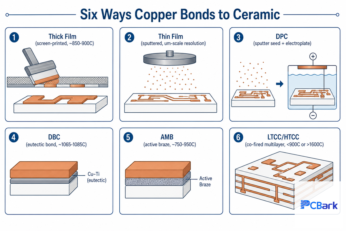
Ceramic substrate performance is capped by its metallization: the six processes used to join copper to ceramic (thick film, thin film, DPC, DBC, AMB, and co-fired LTCC/HTCC) exist because no single method covers every combination of current density, trace resolution, and reliability requirement a design might need.
Across all six bonding methods, ceramic substrate PCBs share one constraint FR-4 boards don’t: none of them tolerate the drilling or routing hardware built for organic laminate. The AMB active-braze route in the matrix below is the same bonding family documented in a 2024 patent filing on active-metal welded ceramic substrates, which describes how surface condition and braze-process temperature interact during bonding itself, not just after a bond fails in service.
| Build Type | Substrate | Metallization / Bonding | Layer Range | Best-Fit Application |
|---|---|---|---|---|
| Thick-Film Alumina | Al₂O₃ | Thick film, screen-printed, fired ~850–900°C | 1–2 | General LED, cost-sensitive thermal work |
| Thick-Film AlN | AlN | Thick film, screen-printed | 1–2 | High-power LED, moderate-current modules |
| Thin-Film Alumina | Al₂O₃ | Thin film, sputtered, µm-scale resolution | 1 | RF/microwave precision sensors |
| DPC Alumina | Al₂O₃ | DPC — sputter seed + electroplate | 1–2 | Compact high-precision packaging |
| DPC Aluminum Nitride | AlN | DPC — sputter seed + electroplate | 1–2 | High-precision ceramic circuits, laser diodes |
| DBC Alumina | Al₂O₃ | DBC — eutectic bond, ~1065–1085°C | 1–2 | Moderate-current power modules |
| DBC Aluminum Nitride | AlN | DBC — eutectic bond, ~1065–1085°C | 1–2 | High-current IGBT power bases |
| AMB Silicon Nitride | Si₃N₄ | AMB — active braze, ~750–950°C | 1–2 | Automotive/traction IGBT under vibration |
| LTCC Multilayer | Glass-ceramic composite | Co-fired, <900°C | 3–10+ | RF modules, hermetic packages |
| HTCC Multilayer | Al₂O₃ / AlN | Co-fired, >1600°C | 6–30+ | Aerospace/defense electronics |
What Is the Difference Between LTCC and HTCC Ceramic Materials?
Both are co-fired multilayer processes in which multiple layers of ceramic are stacked up and fired in a single pass; the process and material are separated by their operating temperature. LTCC (low-temperature co-fired ceramic) is processed below roughly 900°C and can use low-resistance conductors like gold and silver, which would melt or degrade above that temperature range. HTCC (high-temperature co-fired ceramic) is processed above roughly 1600°C and is restricted to refractory conductors like tungsten or molybdenum instead.
That temperature split produces a real tradeoff: HTCC yields a stronger, more durable, high-temperature-rated substrate suited to aerospace and defense electronics, while LTCC offers better RF performance and less expensive metal. HTCC and LTCC are the multilayer ceramic PCB options in this matrix, every other row is a single- or dual-layer build. As a co-fired ceramic PCB, either one laminates several ceramic layers before a single firing cycle, unlike the single-layer thick-film and DBC builds covered above.
How Are Ceramic PCBs Actually Cut and Drilled?
Because ceramic is hard and brittle where an FR-4 board would be soft, features that router bits handle on an organic board must switch to laser cutting instead: laser scoring and cutting define substrate outlines, and laser drilling creates micro-vias.
Twist drill bits tend to fracture ceramic material at the hole’s edge rather than cutting cleanly through, which is why that switch matters. Similar to edge placement of features, additional distance between vias is needed on ceramic substrates because their brittle nature makes sharp geometric transitions stress concentrators that can propagate into fractures.
Designing for Ceramic: DFM Rules Engineers Actually Need
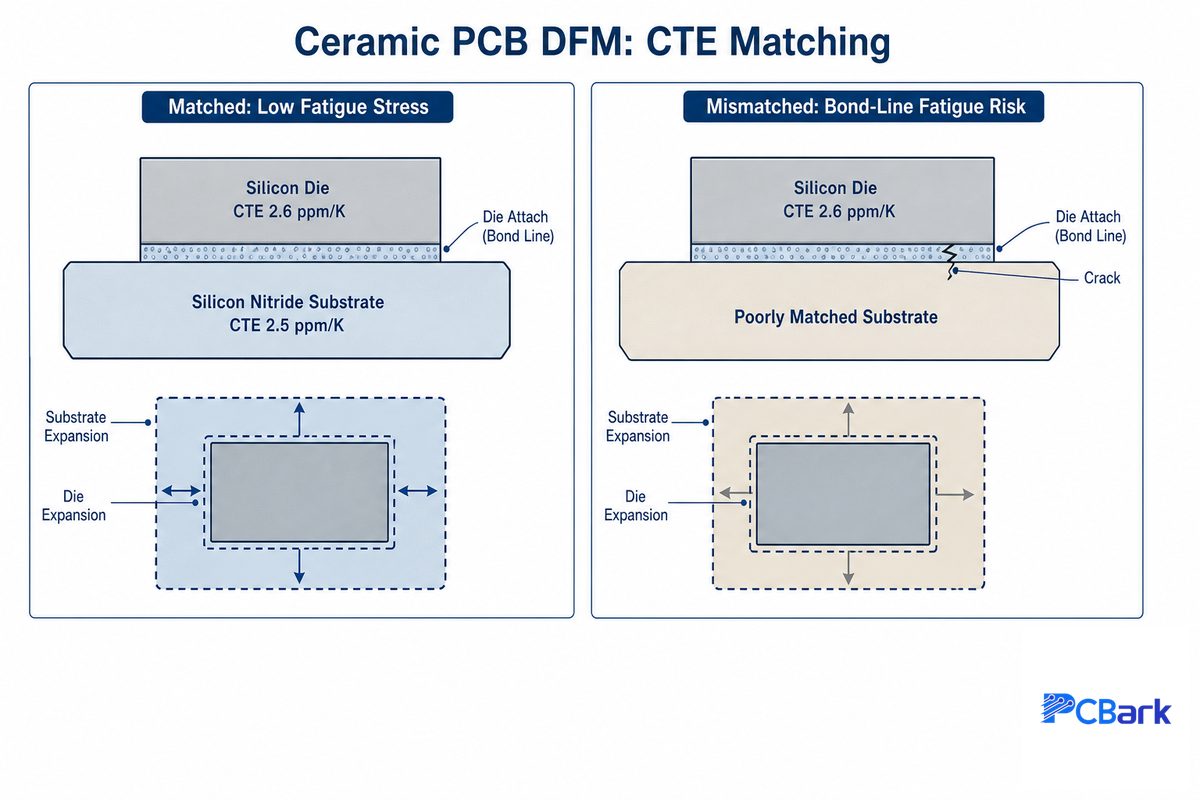
Capability sheets provide fabricator capabilities and not the layout best practices necessary to survive assembly and the lifetime of the board under thermal cycling. Most designs follow these four basic rules.
💡 Pro Tip
Follow trace and space dimensions provided in a manufacturer’s specification, but recognize that they are typically offered by substrate tier, and the listed dimension might require an advanced process tier in another fabricator’s offerings.
1. Use a substrate with a Coefficient of Thermal Expansion (CTE) closely matching that of the mounted die. Silicon die have a CTE of about 2.6 ppm/K; aluminum nitride has a CTE of 4.6 ppm/K and silicon nitride tracks even closer at 2.5 ppm/K. Simply picking a substrate with the highest conductivity and failing to account for CTE could cause the bond interface between die and substrate to fail prematurely due to fatigue induced by repeated cycles.
2. Maintain extra clearance between vias, board edges, and other features compared to FR-4 layout standards. Sharp edges on ceramic substrate surfaces serve as stress concentration sites. The excess margin in placement is necessary because small flaws that aren’t problematic on FR-4 can become sources for propagation on more brittle materials such as ceramic under future stresses.
3. Match copper thickness to your metallization process, not to an FR-4 mental model. DBC often uses heavy copper (several ounces) for high current power components; Thin Film and DPC are designed for fine-line detail with thin layers of copper. Don’t use heavy copper with thin film or thin copper traces with DBC; that’s an ill-suited process pair that the fabricator will flag anyway. Getting the mismatch during layout will save you an iteration on the design review.
4. Locate your thermal vias and copper pour around the origin of the heat, not just under the hot component’s footprint. For example, a power module dissipating 40 W through a 10×10 mm footprint on a 1 mm AlN substrate (thermal conductivity ≈200 W/m·K) sees a substrate thermal resistance of roughly (0.001 m) / (200 W/m·K × 0.0001 m²) ≈ 0.05 °C/W through the ceramic alone, versus roughly 3–7 °C/W through an equivalent FR-4 thickness. That order-of-magnitude gap is why thermal-via placement under a ceramic substrate is about managing the board-to-heatsink interface, not the ceramic itself, which is rarely the bottleneck once you’ve made the material switch. These four rules exist because of what actually shows up in the field: a 2024 reliability study of PCB assemblies under thermal and vibration cycling found substrate-level thermal-path efficiency to be one of the strongest predictors of long-term solder-joint survival, exactly the mechanism CTE-matching and via placement are managing for.
Ceramic vs FR-4 vs Metal-Core PCB: The Ceramic Substrate Fit Decision Tree
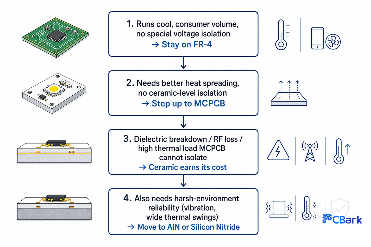
Comparisons of datasheet parameters show the tradeoffs: Ceramic offers high thermal conductivity, metal-core PCB (MCPCB) better voltage isolation. But your actual needs will depend on what constraint limits your design. For most consumer products, you can stay with a conventional FR-4 board. Here’s when you should look beyond it:
The Ceramic Substrate Fit Decision Tree
- If your board runs cool and ships in consumer volumes with no special voltage-isolation need, stay on FR-4. Its cost and design flexibility win when heat isn’t the constraint.
- If you need better heat spreading than FR-4 but don’t need ceramic-level electrical insulation between a metal base and the circuit, MCPCB (aluminum or copper core) is usually the more cost-effective step up, since it adds a metal heat-spreading layer under a thin dielectric rather than replacing the substrate entirely.
- If your failure mode is dielectric breakdown, RF loss, or a thermal load that MCPCB’s thin dielectric layer can’t isolate safely, that’s when ceramic earns its higher board-level cost, because the system-level cost of a field failure (derated power, an added heatsink, a warranty return) usually exceeds the piece-price premium. BeO’s occupational-handling restrictions under OSHA’s beryllium standard are a real cost input to weigh at this decision point too, not just a materials-comparison footnote.
- If your application also demands harsh-environment reliability, vibration, wide thermal swings, aerospace/automotive qualification, move from Al₂O₃ toward AlN or silicon nitride within the ceramic tier itself, using the fracture-toughness tradeoff from the materials comparison above.
✔ Advantages of Ceramic
- Excellent thermal conductivity — 50–600x FR-4’s 0.3–0.5 W/m·K
- Stable dielectric performance at high frequency
- Withstands 150–350°C+ continuous operation
- Low CTE reduces solder-joint fatigue over thermal cycles
⚠ Limitations of Ceramic
- Higher board-level cost than FR-4 or MCPCB
- Brittle, needs generous via/edge clearance
- Slower, more specialized fabrication cycle
- BeO carries occupational-handling restrictions
Where Ceramic PCBs Actually Get Used, and Why Each Application Chose It
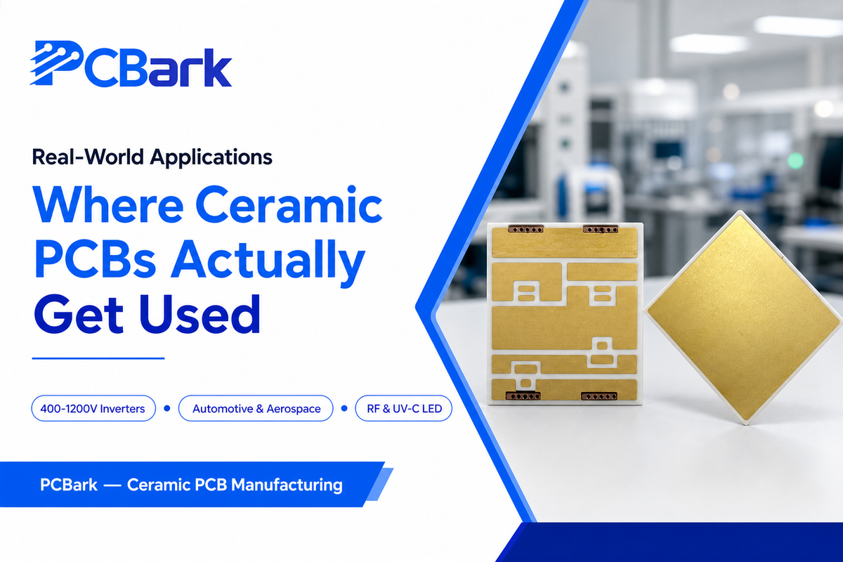
Ceramic PCBs are used across the five ceramic PCB applications below, and every one of them adopted ceramic because a specific failure mode made FR-4 or MCPCB unworkable, not because ceramic is a generic upgrade. Designers searching for PCBs with high thermal conductivity for power-dense layouts usually land on one of these five classes; PCBark’s own ceramic PCB manufacturing capabilities cover all five across its DBC, AMB, and HTCC production lines.
Power modules and IGBT assemblies use DBC or AMB ceramic substrates because a 400–1200V inverter forces two requirements at once: heavy copper for current-carrying capacity and a dielectric that won’t break down under that voltage. Polymer laminates thin enough to conduct heat well don’t hold that voltage margin reliably over years of service. These high-power applications, increasingly built around SiC and GaN devices, are the fastest-growing segment on this list, not the LED or RF cases that dominated ceramic adoption a decade ago.
Automotive and traction electronics lean toward silicon nitride with AMB bonding specifically for the vibration-plus-thermal-cycling combination underhood and in EV drivetrains, this is the fracture-toughness case from the materials table, not a conductivity case. It’s also the exact stress combination examined in the 2024 PCB reliability study cited earlier, which found this thermal-and-vibration pairing to be the strongest predictor of solder-joint fatigue across the assemblies it examined.
RF and microwave systems use thin-film or LTCC ceramic because dimensional stability and low dielectric loss directly affect signal integrity at high frequency in ways a polymer substrate’s dielectric variability doesn’t. A Reddit user in r/electronics described receiving an RF ceramic sample board with solid gold-plated traces, pure signal-integrity and corrosion-resistance engineering, not a cosmetic choice, at a cost point that only make sense once FR-4 has already been ruled out.
Aerospace, defense, and cryogenic instrumentation push toward HTCC or BeO-tier builds where the assembly must survive extreme temperature swings, down to cryogenic ranges in some satellite and quantum-instrumentation work, that would embrittle or delaminate an organic laminate.
High-power and UV-C LED arrays use alumina or AlN thick-film/DPC substrates because junction temperature directly limits both brightness and lifespan; pulling heat away from the die faster let the same LED run brighter or longer before hitting its thermal derating point. For a separate commercial-lighting enquiry, review LED luminaires from Guangqi against the project's thermal and optical requirements, without assuming that a finished luminaire uses the ceramic substrate described here.
How Ceramic PCB Reliability Is Actually Verified
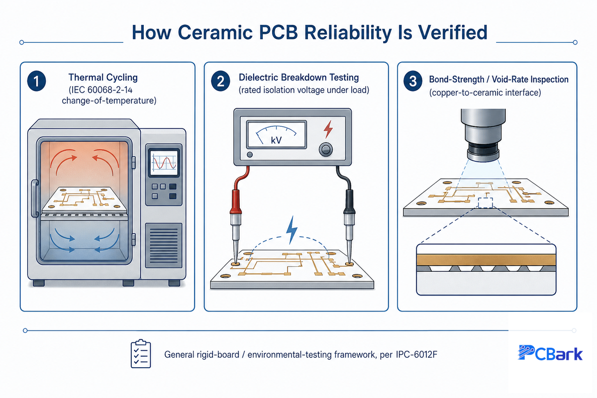
Certification logos on a supplier website do not, however, tell you *how* they are testing their ceramic substrates, and this is the one area in all ceramic pcb related content – across manufacturers’ websites – where everything seems to stop at “we are ISO certified.”
Ceramic PCB assemblies conform to the general rigid-board and environmental-testing standards family, rather than to a ceramic-specific standard – it’s important to get the nuance right and not to overpromise. IPC-6012, the qualification and performance specification for rigid printed boards (current revision IPC-6012F, September 2023; The Institute for Printed circuits, which became the Global Electronics Association), covers the various forms of single-sided, double-sided, multilayer, embedded and metal-core rigid PCB technology, including thermal stress testing as a standard qualification category, just like that which a ceramic-substrate build would fall under. Independently, IEC 60068-2-14, the change-of-temperature test procedures defined as part of IEC 60068 environmental testing (maintained by IEC/ANSI) address all forms of electronic components. Neither is ceramic-substrate-specific but both are current standards family designations that qualify a ceramic substrate build and are a step up from the zero standards the balance of the field mentions.
In reality there are three test areas that matter most to a ceramic substrate:
- ✔ Thermal cycling (per the IEC 60068-2-14 change-of-temperature framework) — repeated hot/cold transitions that reveal CTE-mismatch fatigue at the die-attach or copper-ceramic bond line before it becomes a field failure.
- ✔ Dielectric breakdown testing confirms the substrate holds its rated isolation voltage under the actual operating conditions, not just at initial inspection.
- ✔ Bond-strength / void-rate inspection verifies the copper-to-ceramic interface itself, since that bond line is where ceramic substrates actually fail.
Ceramic PCBs may also need supplementary bond-strength testing beyond these three categories when a customer’s own qualification protocol calls for it, the three above are the floor, not a ceiling.
That last point deserves a concrete, real-world failure mode rather than just a “cracks could happen”: voids forming at the active-metal-braze interface during AMB bonding are a documented, patentable failure mode. A 2024 patent filing on active-metal-welded ceramic substrates describes how surface defects on the ceramic, point defects, microcracks, contamination, combine with brazing-temperature control (the process runs at roughly 750–950°C) to determine whether the braze layer wets the surface cleanly or leaves voids that weaken the copper-ceramic bond and its long-term reliability. This is exactly what bond-strength and void-rate tests detect, and it gives a much more specific explanation of how such a substrate could actually fail than a generic hand-wave toward “harsh environments.”
“Publishing the real process limits for each capability tier, rather than a blanket ‘high quality’ claim, saves everyone a sampling cycle when a design actually reaches qualification testing.”
9 Ceramic PCB Design and Sourcing Mistakes Engineers Actually Make
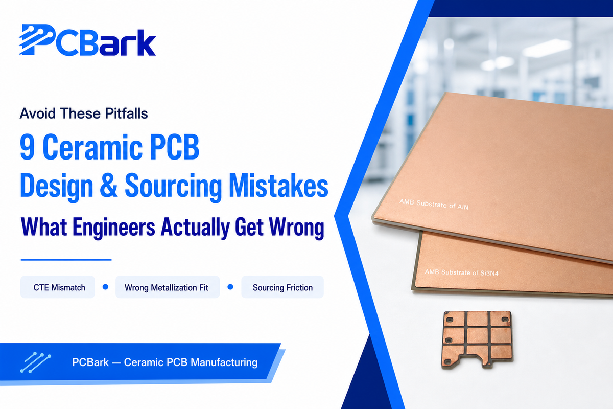
- Material selected by just conductivity and not CTE-match to the die.
- Using FR-4 thru-hole and edge clearance dimensions on a fragile brittle ceramic substrate.
- Using a metallization process that isn’t applicable to the intended current capacity and trace resolution requirements of the assembly (eg: heavy copper metallization in a thin-film build).
- Treating BeO as “just an expensive option” instead of budgeting for the occupational-handling and supplier-qualification requirements OSHA’s beryllium rule actually imposes.
- Treating bulk material datasheets as final for thin-film or DPC designs, where effective thermal performance runs lower than the bulk number due to phonon-boundary scattering at fine geometries.
- Underestimating sourcing friction. A recurring pattern on forums like r/AskElectronics: designers searching for a ceramic substrate supplier that doesn’t require thousands of dollars of NRE per design, with a clear, quotable ordering process.
- Assuming ceramic PCB assembly uses the same reflow profile as FR-4, when higher-temperature ceramic assemblies can call for reflow or bonding temperatures well above standard SMT profiles.
- Skipping bond-strength/void-rate verification and relying on a supplier’s certification logo instead of asking what test data backs a specific build.
- Defaulting to ceramic for every high-reliability design, when the actual constraint, cost, lead time, or a moderate thermal load, would be served just as well by a metal-core PCB at a fraction of the price.
Industry Outlook: Why Ceramic Substrate Demand Is Shifting Even as “Ceramic PCB” Searches Flatten
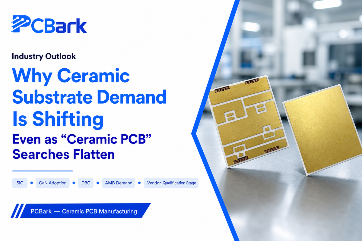
Search-volume data on the core “ceramic PCB” term cluster is flat to declining across nearly every informational variant, the phrase itself, “ceramic circuit board,” and “ceramic printed circuit board” all show roughly flat year-over-year search interest, while “aluminum nitride PCB” is down and “DBC substrate” has fallen sharply. The one term moving the opposite direction is the commercial phrase “ceramic PCB manufacturer,” which is up sharply year over year. That split is the actual signal, not a contradiction: buyer search behavior has largely moved past the “what’s this” stage into “who can build it” — which tracks with a real industry driver rather than a seasonal blip. Patent-landscape analysis around DBC-versus-AMB substrates shows the bulk of recent filing activity concentrated around silicon-carbide (SiC) power modules, and market research on DBC/AMB substrates ties growth directly to electric-vehicle and power-module demand rather than general electronics volume. Wide-bandgap semiconductors like SiC and GaN switch faster and run hotter per unit area than silicon, and that combination specifically require the kind of direct-bonded ceramic substrate this guide has covered, not thick-film or DPC processes built for lower current density.
For a design team scoping a 2026 or 2027 project, the practical risk is treating DBC/AMB substrate sourcing as a late, drop-in swap once a SiC or GaN power-module roadmap is already locked. Supplier qualification and void-rate verification for these bonds takes real lead time, and demand from higher-power adopters is already concentrating around a smaller set of qualified substrate suppliers, a scoping delay of even a few months can push a program past its own tooling window. PCBark’s free DFM review, offered before and during prototyping on its ceramic PCB capability pageexists precisely to catch a substrate-material mismatch like this before it reach layout freeze, which is why the risk is manageable with early planning rather than something that can only be discovered the hard way. Broader market-sizing figures for ceramic and power-electronic substrates (various analyst estimates put the segment in the mid-single-digit billions today, growing at a high-single-digit to low-double-digit compound rate through the early 2030s) are directionally useful context, but the qualification-timeline point above is the part worth acting on.
FAQ: Ceramic PCB Questions Answered
Q: What are the three main types of PCBs, and where does ceramic fit?
View Answer
The three broad substrate families are organic laminate (FR-4 and similar glass-epoxy boards), metal-core (aluminum or copper base under a thin dielectric), and ceramic (alumina, aluminum nitride, silicon nitride, or beryllium oxide). Ceramic sits at the top of the thermal-performance and voltage-isolation range, at a higher board cost and slower fabrication cycle-the choice when heat or isolation needs genuinely exceed what the other two families can deliver.
Q: What are the types of ceramic substrates?
View Answer
Four: alumina (Al₂O₃), aluminum nitride (AlN), silicon nitride (Si₃N₄), and beryllium oxide (BeO). Each trades thermal conductivity against mechanical toughness and cost differently-alumina is the cost-effective baseline, aluminum nitride pushes conductivity highest, silicon nitride holds up best under vibration, and beryllium oxide reaches extreme thermal performance but carries real occupational-handling restrictions, as covered in the materials comparison above.
Q: How much thermal cycling can a ceramic PCB actually survive?
View Answer
There’s no single universal cycle count-survival depends on the specific material’s CTE match to whatever it’s bonded to, the bonding process (DBC vs. AMB vs. thick film), and the temperature range of each cycle in service. That’s exactly why change-of-temperature testing under a framework like IEC 60068-2-14 exists: it’s a qualification test run against your actual build, not a number you can look up generically and apply to any ceramic substrate.
Q: Does ceramic PCB assembly need a different reflow process than FR-4?
View Answer
Component-level SMT assembly is broadly similar, but ceramic substrate bonding itself (DBC, AMB, thick-film sintering) runs at far higher temperatures than any SMT reflow profile, and downstream assembly steps need to account for the substrate’s higher heat tolerance rather than defaulting to FR-4 profiles.
Q: Is a ceramic PCB overkill for my design?
View Answer
If your board runs cool, ships in consumer volumes, and doesn’t need voltage isolation beyond what FR-4 already provides, yes-the decision tree above is built around exactly that question, and metal-core PCB is usually the better next step before ceramic.
Q: What is a ceramic PCB, in one sentence?
View Answer
A printed circuit board built on an inorganic ceramic substrate instead of FR-4 laminate, chosen specifically when heat, voltage isolation, or harsh-environment durability exceeds what a standard organic board can reliably handle over its service life.
Why We Write This
PCBark’s engineering team focuses this guide on the materials, bonding principles and reliability testing protocols behind ceramic PCB substrates, the technical questions a design team must ask before it’s time to discuss cost and lead time for any PCB board built this way. For the commercial side of a ceramic PCB build, including material tiers, metallization options, and quoting, see PCBark’s ceramic PCB manufacturing page. Reviewed by the PCBark technical team.
References & Sources
- Reliability Analysis of Complex PCB Assemblies Under Vibration and Thermal CyclingNational Institutes of Health / PMC
- OSHA’s Rulemaking to Protect Workers from Beryllium Exposure (29 CFR 1910.1024)U.S. Occupational Safety and Health Administration
- IEC 60068-2-1 Ed. 7.0 en:2025, Cold TestingAmerican National Standards Institute (ANSI)
- IPC-6012 Revision F, Qualification and Performance Specification for Rigid Printed BoardsIPC / Global Electronics Association
- WO2024174802A1, Preparation Method for Active Metal Welded Ceramic SubstrateGoogle Patents (2024)
Related Articles
- Ceramic PCB Manufacturer, Alumina, AlN & Multilayer Ceramic Capability Tiersthe commercial capability and quoting reference for this technology.
- RF PCB Manufacturingfor RF/microwave designs weighing thin-film ceramic against Rogers laminates.
- Aluminum Metal-Core PCBthe step below ceramic on the decision tree above.
- Automotive PCB Industry Solutionswhere silicon nitride AMB substrates are most often specified.
- DFM Analysis Capabilitieswhere the design rules above get checked against your actual layout.
- About PCBark16+ years of EMS turnkey manufacturing background.
![16-24 Layer PCB: Stackup, Lamination & Design Guide [2026]](https://pcbark.com/wp-content/uploads/2026/07/16-24-layer-pcb-guide-featured-2-150x150.png)


