Get in touch with PCBark Company

ISO Certified
Heavy Copper PCB
Heavy Copper PCB Manufacturer, Up to 20 oz Copper & 32 Layers
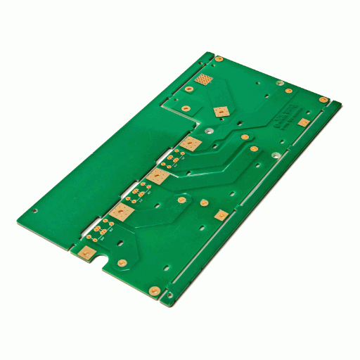
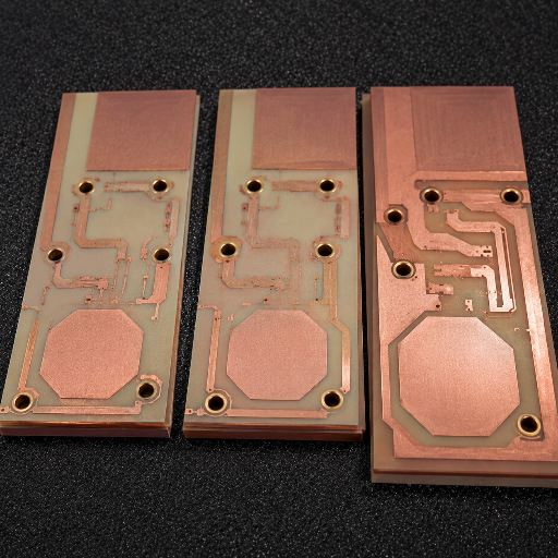
Heavy Copper Designs PCBs can’t hold for standard 1oz. PCBark designs and manufactures Heavy Copper PCBS from 2oz – 20 oz outer copper and up to 32 layer – way over 5 oz to 6 oz outer layer PCBs which is normally limited. Heavy copper is ideal for all power electronic products, EV charging stations and high-current industrial systems.
Request a Quote (RFQ)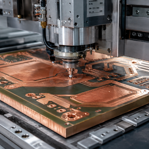
Automation
Finished Board
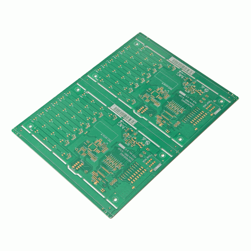
Inner Layer
2–20 oz
Outer copper weight
2–12 oz
Inner copper weight
32
Max layers
6.0 mm
Max board thickness
±10%
Impedance control
600×1200 mm
Max board size
100%
E-test on every board
16 yrs
EMS manufacturing
PCBark Heavy Copper PCB Capabilities, Standard · Best · Maximum
A majority of the heavy copper PCBs manufacturers will only go up to 5 or 6oz. PCBark offers three levels of capability and our extreme capability class – which is called extreme copper – includes 20 oz outside copper, 12 oz inner copper, with up to 32 layers of capability — that extra clearance your industrial high current and new energy program requires. All numbers here were from our available published heavy copper process capability sheet.
| Parameter | Standard | Best | Maximum |
|---|---|---|---|
| Outer copper thickness | 2–4 oz | 4–8 oz | 20 oz |
| Inner copper thickness | 2–4 oz | 4–6 oz | 12 oz |
| Finished copper | 70–140 µm | 140–280 µm | 560 µm+ |
| Layers | 2–8 | 4–16 | 32 |
| Board thickness | 1.0–3.2 mm | 1.6–4.0 mm | 6.0 mm+ |
| Min. trace / spacing | 0.20 / 0.20 mm | 0.15 / 0.15 mm | copper-dependent |
| Min. hole size | 0.30 mm | 0.25 mm | 0.20 mm |
| Hole copper | ≥25 µm | ≥35 µm | ≥50 µm |
| Surface finish | HASL-LF, OSP | ENIG, HASL-LF, OSP | ENIG, Imm. Silver/Tin, Hard Gold |
| Impedance control | ±10% | ±8% | ±5% |
| Max board size | 400×500 mm | 500×600 mm | 600×1200 mm |
Which tier fits your board?
| If your design needs… | Recommended tier | Typical use |
|---|---|---|
| Medium-to-high current, 2–8 layers | Standard (2–4 oz) | Power & control boards |
| High-current power modules, 4–16 layers | Best (4–8 oz) | Industrial PSU, automotive, inverters |
| Busbar-grade current, mixed copper, ≤32 layers | Maximum (up to 20 oz) | New energy, storage, EV chargers |
Substrate, finish & build options
The success of heavy copper isn’t solely a function of how thick is the copper-the substrate carries its heat along for the ride. For standard, main stream power boards-and we’ll touch upon special applications later-PCBark constructs its heavy copper on both FR-4 and HighTg FR-4, building on ROGERS® or polyimide based hybrid materials or metal core bases when the substrate must endure sustained high temperatures. As we build up multilayer PCBs having ever heavier copper in each, solder masks become more defined, trace lines tighten, inner-layer registration improves-and so heavy copper PCB manufacturing is as much about substrate FR-4, plated via thickness and PCB lamination as about the metal itself. Heavy copper PCB build-up by electroplating is detailed in heavy-copper PCB patents such as CN104853523A. Heavy copper PCB designs rely on electroplating for their creation, but the pairing of substrate material thickness with heavy copper must be balanced carefully where heat dissipation, thermal management, and the copper traces that move the current are all critical.
Heavy Copper PCB Vs Standard PCB, And Vs Volume Platforms
Why Insist On Heavy Copper - There’s A Definite Reason - Measured, Not Hype.
On a 10-mil trace with a 10C temperature rise, for example, the current that 3-oz copper will carry, compared to 1-oz copper, increases from approximately 1.2 amperes to over 3.5 amperes - just shy of a 3X improvement from a 3X increase in copper thickness. Thicker copper also improves heat dissipation and spreading and gives extra mechanical resilience to shock and vibration.
| Attribute | Standard 1 oz PCB | Heavy Copper (3 oz) | PCBark Maximum (up to 20 oz) |
|---|---|---|---|
| Current (10-mil, 10 °C rise) | ~1.2 A | ~3.5 A | Busbar-grade |
| Finished copper | ~35 µm | ~105 µm | up to 560 µm+ |
| Heat spreading | Limited | Strong | Highest |
| Max layers | typ. 2–8 | up to 16 | 32 |
| Relative board cost | baseline | +30–50% | quote-based |
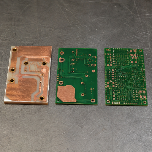
There’s One Second Comparison That Customers Bring Up More Than Anything Other Than One Of Our Specs - Cheap Volume.
The fixed profile prototype houses work within tightly defined constraints, and standard clearances widen with copper weight and trying to order 2 oz on some of them would put you forced to push a minimum trace from 5 mil to 8 mil before they will even quote. Standardization is the core their business and at the expense of ability, it’s the perfect service for two layer boards, however it's the exact opposite for the power you've so why even bother? For a high power pcb that needs 8 oz or more, that trade-off is disqualifying. High-current thick-copper construction is covered in filings such as CN203537662U. PCBark’s operation is reversed to this: Thick copper plating and etch control is the heart of the business so our standard 8oz, 12 oz, 20 oz panels stay in tolerance.
+30–50%
Typical board-cost premium moving from 1 oz to 3 oz copper — offset against the field-failure cost of an under-spec'd trace.
Source: industry pricing analysis (ALLPCB, 2025). Exact pricing is design-specific — request a quotation.
Copper Weight & Current-Carrying Capacity, How to Spec Your Board
A heavier board isn’t necessarily a hotter-current board. On the bench, folks sometimes figure 4 oz copper, just by itself, ‘carries a whole heap of current.’ But its actual capacity to carry that current is based on that IPC-2152 chart and what balance of width and allowable temperature rise the board designer want. Choose copper weight for the current that you actually want to carry, then check your trace width to the standard. The trade-off, however, is real: heavier copper is good for current and bad for width.
Engineering Note, copper weight, width & the 50% rule
Copper weight is reported in ounces/sq. foot: 1 oz = 1.37 mil (35 µm), 3 oz = 4.13 mil (105 µm) are the industry standard values of these weights. The published data in IPC-2152 for current vs. temp rise (as below) is used for sizing, but when an EE starts to lay out a heavy copper pcb, they reach for a trace width calculator and a copper weight chart and the current-capacity data in IPC-2152, with heavy-copper plating methods documented in patents such as CN105472900A; The real trick is that this is a baseline, it's not fact. there are two Rules of Thumb: copper traces on inner layers have only about 50% the current capacity of traces on outer layers (all other things equal). Also, that "constant steady-state ampacity" assumption doesn't hold for current pulses. A continuous 30 Amp Bus vs. a pulse of 30 Amps, etc.
It even impacts the etching by going a more hefty wire: bigger weights need much more area in between to eliminate nicely - thus the actual heavy-copper restriction at a fabricator is process control, definitely not exactly what the data-sheet says; your real heavy-copper restrict is considerably thinner… We preserve a 20% trace width tolerance for the Standard level… it gets tighter into 10% for optimum. Impedance is maintained within 5%-the panel which you simulate is the panel that you can get; it's that basic!
"On thick copper we design to the IPC-2152 curve first, then to the etch. A 10 oz board that ignores spacing-to-copper ratio looks fine in CAD and fails the cross-section. We hold the ratio so the high-current traces survive thermal cycling, not just the e-test."
Applications, Power, Automotive, New Energy & EV Charging
Heavy copper PCBs appear in applications wherever current density and thermal load are the binding constraint - from a power supply on a factory floor to a 200A charging stage. In battery management systems, motor controllers, and charging infrastructure, working currents can exceed 200A, and the copper plane is doing as much thermal management work as electrical. PCBark's heavy copper boards ship into four clusters:




Quality, Certifications & Testing
Buyers audit a heavy copper PCB manufacturer before they order - formal supplier-evaluation checklists are standard practice, and the failure stories that circulate (inner layers omitted, boards bricked, refunds refused) are trust problems, not just quality problems. PCBark answers that audit with certificates and a test chain, not adjectives — its quality system is certified to ISO 9001.
Global Compliance
ISO 9001
Quality management system
IPC-A-610
Class 2 / Class 3 acceptance
UL
Recognized component
RoHS / REACH
Material compliance
High-Reliability Standards
For high-reliability programs, the relevant bar is IPC-6012 Class 3, which forbids copper-layer gaps and requires through-hole copper fill of at least 75% - strict rules that exist precisely because heavy-current boards fail catastrophically when they fail.
PCBark's heavy copper test chain scales with tier:
| Tier | Test method |
|---|---|
| Standard | 100% electrical test (E-test) |
| Best | AOI + flying-probe + fixture test |
| Maximum | AOI + E-test + impedance + reliability test |
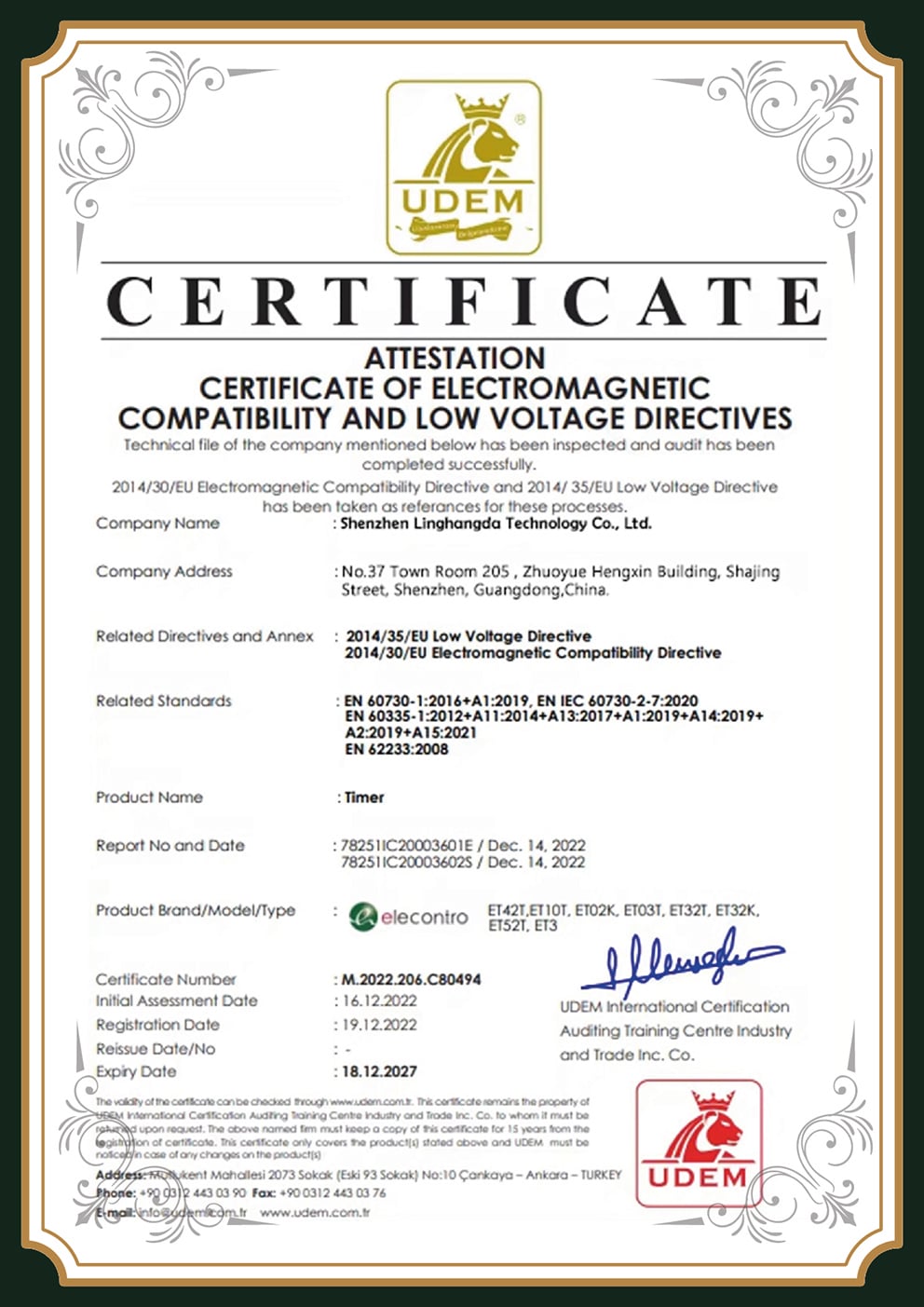
CE Certification
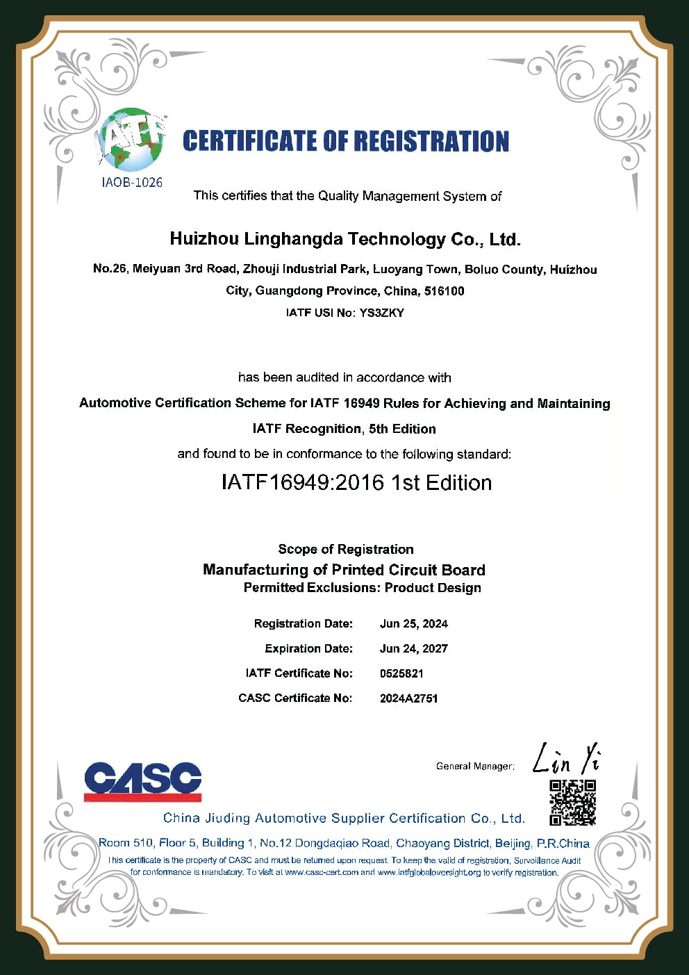
IATF 16949
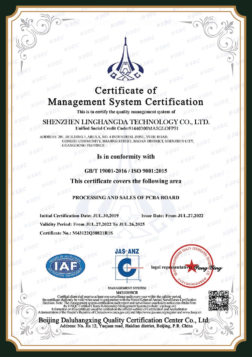
Assembly ISO 9001
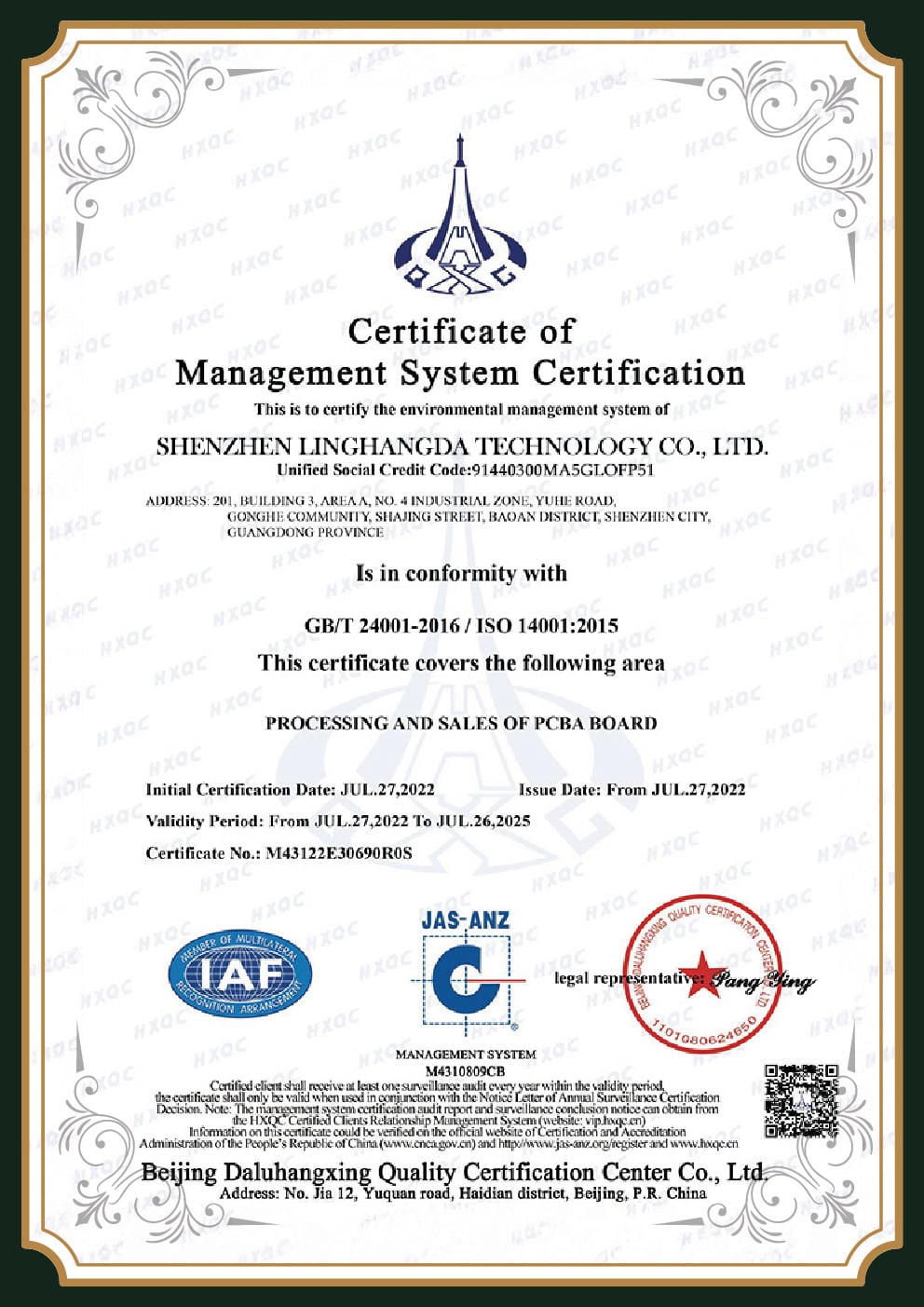
Assembly ISO 14001

PCB ISO 14001

PCB ISO 9001
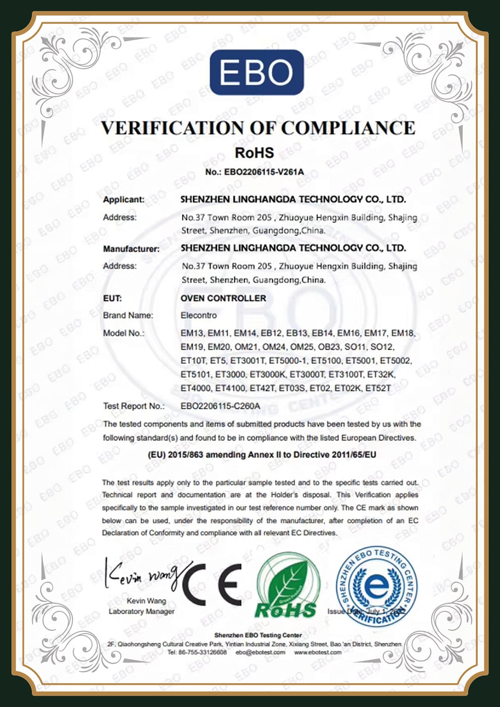
RoHS Compliance
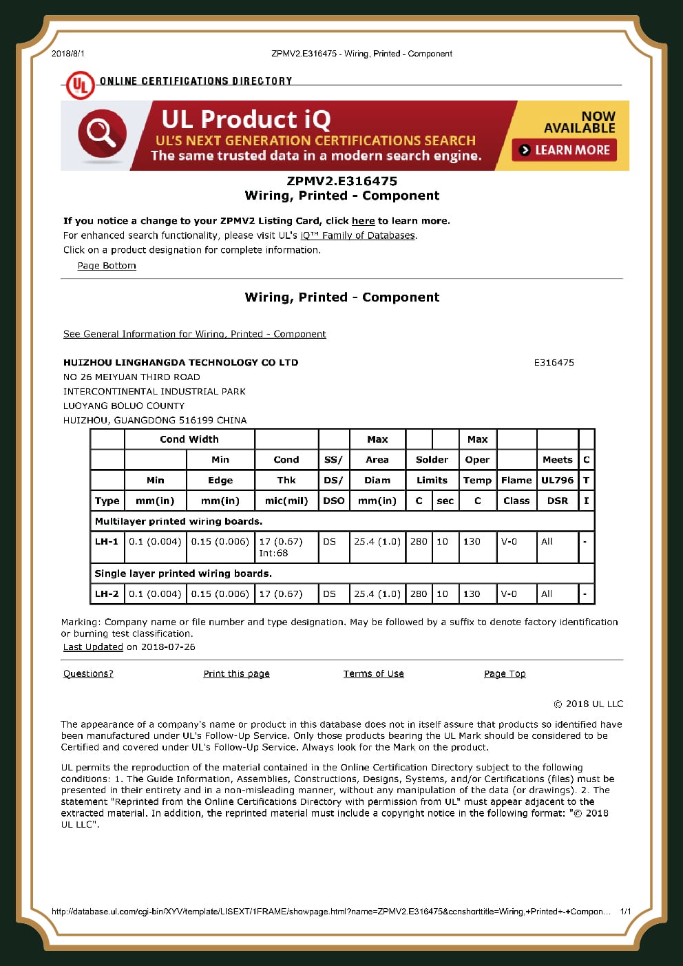
UL Certification
×
![Enlarged Document]()
Procurement Guide, Lead Time, MOQ & What Drives Heavy Copper Pricing
Heavy copper pricing isn't a single number - it's a stack of factors, and a quote that hides them usually hides risk. Rather than a list price, here's the pricing-factor framework PCBark quotes against, so you can see exactly what moves your cost before you commit.
Send a Gerber and a target current, and you get a tier recommendation, a DFM note, and an itemized quote.
Heavy Copper PCB Engineering Tools
Heavy Copper Trace Current Calculator
Estimate the current a trace can carry using the IPC-2221 relationship between copper weight, trace width, and temperature rise. For production design, PCBark verifies against IPC-2152.
Open Tool
Heavy Copper PCB Tier Selector
Match your current, layer count, and application to a PCBark capability tier — Standard, Best, or Maximum.
Open Tool
Copper Thickness Converter — oz · µm · mil
Convert copper weight between ounces per square foot, microns, and mils. Heavy copper starts at 3 oz; PCBark builds up to 20 oz.
Open Tool
Heavy Copper PCB FAQ
Heavy copper PCBs are a higher-gauge form of printed circuit board that carry 3 ounces of copper or greater on one (or more) copper layer-vs 1oz typically-to facilitate far higher current handling and better heat sinking. PCBs designed for high current come to us from 2 oz up to 20 oz.
To 20 oz on outer layers, 12 oz on inner layers. Finish 560 um (or more). As many as 32 layers. (We build beyond the 5-6 oz max for which most conventional heavy copper manufacturers limit their capabilities).
It depends not solely on finish copper thickness, but more significantly on trace width and permissible temperature rise per IPC-2152. For a rough, one-off comparison: a 10 mil trace with a 10 deg. C rise handles ~1.2 Amps when 1 oz. For 3 oz copper, a 10 mil trace can carry ~3.5 amps at the same temperature rise. Just send us your targeted amps, and we'll specify how much copper you'll need.
At 560 m (22 mil), a little less than three times the 35 m of 1oz copper at the equivalent layer-count designation.
Standard prototyping services exist at scale under tight manufacturing process rules for efficiency, leading to minimal material option sets and standard fabrication practices that lack depth when applied to thicker copper products (maxed out at 5-6 oz most anywhere else). This also explains the wide ranges on certain board specifications where there isn't simply one standard product available. However, a heavy copper specialist provides deep experience with specialized etching and plating processes allowing for tight control even with high copper weights.
Rigorous Quality Control: ISO 9001, ISO9001 certified. IPC-A-610 Class 2 and Class 3 accepted. UL certification and RoHS/REACH compliant. Class 3 build specification, per IPC-6012, for applications requiring extremely high reliability.