Get in touch with PCBark Company

ISO Certified System
IoT PCB (PCBark brand)
IoT PCB Manufacturing & Assembly for Connected Devices
An IoT PCB is the printed circuit board at the core of every connected device, the layer where battery life, wireless range, and field reliability are actually won or lost. PCBark builds these boards end to end: HDI and rigid-flex fabrication, IPC-A-610 Class 2 and Class 3 assembly, low-power DFM review, and wireless module sourcing, from a 20-piece prototype to volume production.
1–40 layer count (HDI & UHDI)
3/3 mil min trace/space (2/2 HDI)
±10% / ±5% controlled impedance
0201 / 01005 fine-pitch placement
Wi-Fi·BLE·LoRa·NB-IoT·Zigbee·Thread wireless protocols built
MOQ 1 prototype, volume tiers
16+ years
EMS experience
500,000 sqm/yr
production capacity
IPC-A-610
Class 2 & 3
<10µm accuracy
01005 placement, Turnkey DFM + sourcing + test
Why IoT Boards Fail in the Field, and How Board-Level Design Fixes It
The Core Issue
IoT boards fail in the field for three board-level reasons: a deep-sleep current path that leaks milliamps instead of microamps, an antenna detuned by ground copper sitting underneath it, and wireless traces with no controlled impedance. Each one is fixed in the layout before fabrication, not in firmware afterward, which is why the board, not the bill of materials, decides whether a connected device last five years or five days.
Two IoT trackers can use the same LTE-M radio, the same battery, and the same enclosure, yet ship with wildly different field results. The difference is rarely the bill of materials. It’s the IoT PCB design underneath it: the deep-sleep current path, the antenna ground counterpoise, and the impedance discipline on the wireless traces.
What is an IoT PCB?
An IoT PCB is a printed circuit board engineered for connected devices in the Internet of Things — a single interconnect that ties together sensors, a microcontroller, wireless connectivity (Bluetooth, Wi-Fi, Zigbee, LoRa or cellular), and power management, built for low power consumption, small size, and long-term reliability. Every IoT device shipped today depends on this board; unlike a standard FR-4 design, IoT PCB design is tuned around microampere sleep current, RF signal integrity, and miniaturization rather than raw throughput.
Common Failure
The most common failure we see in incoming designs is battery life. Engineers expect a sensor node to idle in the microampere range, then measure 1.5–2 mA while it’s supposed to be asleep, a 1000× budget miss that drains a coin cell in days. Whether you call it an IoT circuit board, a PCB in IoT, or simply an IoT PCB design problem, that leak lives in the copper, not the code. One designer on a low-power forum put it plainly:
“Since it lasted about 3–4 days being in deep sleep most of the time, I expected a current draw to be 1.5mA to 2mA while sleeping.”
The Board-Level Fix
The root cause is usually a leakage path the schematic never shows: a pull-up tied to a rail that never sleeps, a regulator with high quiescent current, or a sensor left powered between reads. The fix is a board-level power architecture, gated power domains, an ultra-low-quiescent regulator, and a real-time-clock wake path, reviewed before fabrication, not after. Proof it works: current wireless MCUs hold System-Off current to 0.8 µA (Nordic nRF54L) and 0.9 µA with RAM retention (Silicon Labs xG27), and well-designed asset trackers run 3–5 years on a single primary cell by combining that microampere floor with event-driven reporting. Battery endurance is engineered into the copper and the power tree, not bought with a bigger cell. Our PCB assembly line treats that power-path review as a standard DFM step, not an upsell.
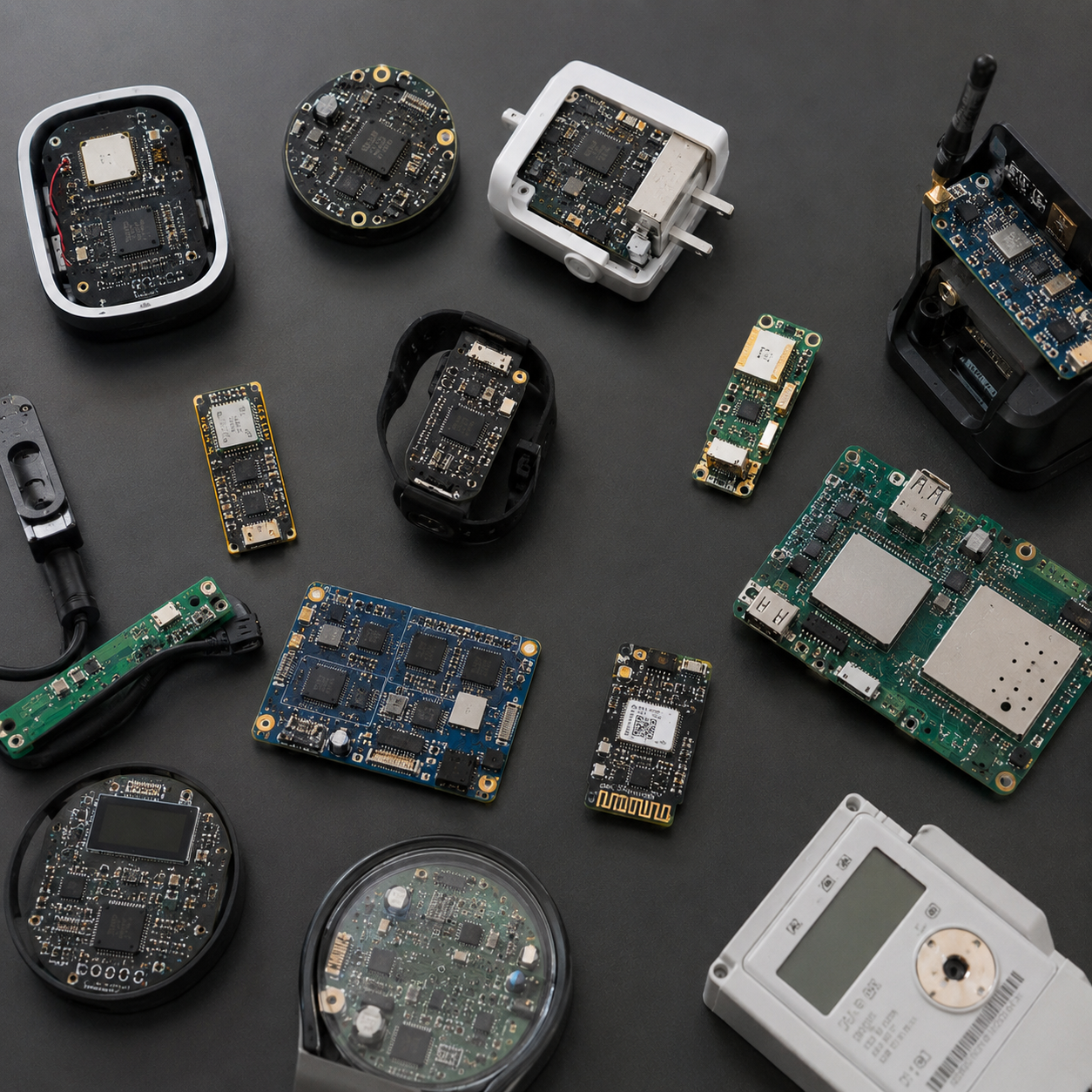
PCBark IoT Manufacturing Capabilities, Fab, Assembly & DFM
An IoT program lives or dies on whether one partner can fabricate the bare board, place the fine-pitch parts, source the wireless modules, and test the result, without three vendors pointing fingers when a board comes back dead. PCBark runs all of it under one roof and one quality system. IoT boards mix a sensitive analog and RF front end with noisy digital switching, so our PCB design and manufacturing flow separates the analog ground, controls the routing impedance on high-speed nets, and places the voltage regulators and power ICs to keep switching noise off the radio. Both tables below are the working capability envelope we build to; every number is an industry-standard, IPC-referenced capability, and the controlled-impedance and 01005 placement figures are confirmed achievable for miniaturized IoT boards.
| Parameter | Standard | Advanced (IoT / HDI) |
|---|---|---|
| Layer count | 1–12 | up to 40 (HDI / UHDI) |
| Min trace / space | 3 / 3 mil | 2 / 2 mil (UHDI ≤50µm) |
| Min mechanical hole | 0.2 mm | 0.1 mm laser microvia |
| Board thickness | 0.4–3.2 mm | 0.16 mm flex / up to 6.0 mm |
| Controlled impedance | ±10% | ±5% (RF / high-speed traces) |
| Surface finish | HASL / OSP | ENIG, ENEPIG, Immersion Ag |
| Material | FR-4 (Tg 150–170°C) | high-Tg, rigid-flex (PI), RF laminate |
| Parameter | Capability |
|---|---|
| Min component | 0201 standard, 01005 (0.4 × 0.2 mm) advanced |
| Placement accuracy | < 10 µm, vision-aligned pick-and-place |
| BGA / package | BGA, micro-BGA, CSP, QFN, 0.4 mm pitch |
| Soldering | lead-free SAC305 reflow, N₂ atmosphere; leaded on request |
| Inspection | SPI + AOI + 2D/3D X-ray (BGA) + ICT + functional |
| Wireless modules | ESP32, nRF52/nRF54, SX126x LoRa, SIM7080 — auth-distributor sourcing |
| Conformal coat / box build | acrylic / urethane / parylene, full turnkey |
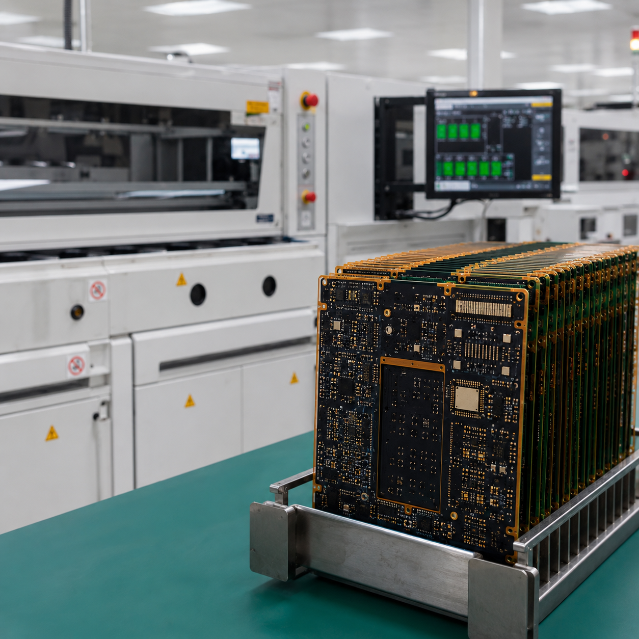
These design considerations, power efficiency, RF isolation, and miniaturization, are the design strategies that separate a reliable IoT PCB from a board that merely powers on. We build them into high-performance IoT devices from the first stack-up, and the same flow serves smart devices, wearable technology, and Industrial Internet of Things (IIoT) nodes alike. Component choices run from passive electronic components to the power management integrated circuit (PMIC) and System in a Package (SiP) modules an IoT device needs.
Engineering note, why 01005 matters for IoT
Wearables and sensor tags reach their size targets by moving to 01005 passives (0.4 × 0.2 mm, among the smallest commercially available) on HDI microvia stacks with via-in-pad. That placement is routine for a current-equipped line but demands <10 µm accuracy, laser-cut fine-aperture stencils, and 3D AOI, capability you should confirm a vendor actually holds before committing a miniaturized board. Our smaller-feature work pairs naturally with HDI PCB stack-ups and, for high-current IoT power stages, heavy copper sections on the same board.
“We review the power tree and the RF section before a single board is fabricated, on IoT designs the cheapest defect to fix is the one we catch in the Gerbers, and the most expensive is the one a customer finds in the field three months later.”
Wireless Connectivity, Engineered at the Board Level
Most IoT PCB design problems that look like firmware bugs are really RF layout problems. The dominant performance metric in a crowded 2.4 GHz building isn’t range, interference rejection decides it, and that’s set by the antenna keep-out, the ground counterpoise, and the impedance of the feed line. The Wireless Protocol Design-Constraint Index below maps each common IoT protocol to the board constraints it imposes, so the stack-up is right the first time.
| Protocol | Band | Feed impedance | Antenna ground need | Board constraint | Best for |
|---|---|---|---|---|---|
| BLE / Thread | 2.4 GHz | 50 Ω | ≥ λ/4 ≈ 31 mm | 3D keep-out all layers | wearables, sensors |
| Wi-Fi (2.4/5) | 2.4 / 5 GHz | 50 Ω | large continuous ground | controlled-impedance feed | gateways, cameras |
| Zigbee | 2.4 GHz | 50 Ω | ≥ λ/4 counterpoise | mesh node isolation | smart home mesh |
| LoRa / LoRaWAN | sub-GHz (868/915) | 50 Ω | larger counterpoise | low-loss feed, via fence | long-range IIoT |
| NB-IoT / LTE-M | cellular | 50 Ω | SAW + matching network | RF/digital isolation | asset trackers, meters |
| NFC | 13.56 MHz | tuned LC | coil keep-out | loop antenna clearance | access, pairing |
Buyer advisory, the antenna mistake that detunes 2.4 GHz boards
Antenna keep-out is a 3D cylinder through every layer, not just the top. The frequent error is clearing copper on the top layer while ground planes, power planes, or traces stay on the inner and bottom layers directly under the antenna, which detunes it and shifts the resonant frequency. A surface-mount chip antenna also needs roughly a quarter-wavelength of continuous ground (about 31 mm at 2.4 GHz) to radiate efficiently, so shrinking an IoT board too far directly degrades wireless range. We flag both at DFM. For designs that push into true RF or microwave laminate territory, our RF & microwave PCB capability covers the material side.
Here’s the honest answer most shops won’t give:
you usually don’t need an exotic low-Dk laminate to run wireless. At 10 GHz, standard FR-4 carries about four times the dielectric loss of a high-Dk PTFE laminate, which means dielectric constant is the wrong selection driver, and RF can route cleanly to the gigahertz range on a 2-layer grounded coplanar waveguide with a via fence. We right-size the material to the design instead of upselling PTFE on every board. Reliable wireless communication across a wireless network depends on this radio frequency (RF) discipline at the integrated circuit and antenna interface, not on exotic laminate.
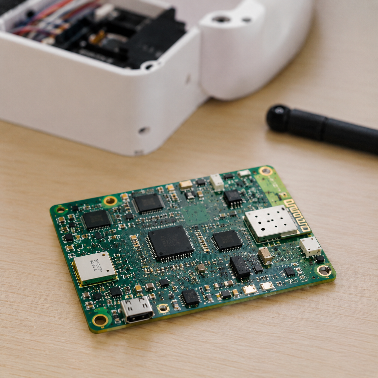
IoT PCB vs Standard PCB, and the Real Cost of Getting It Wrong
Procurement teams usually compare IoT board quotes the way they compare commodity boards: lowest unit price wins. That math breaks on connected hardware, because the dominant cost isn’t the fab invoice, it’s the redesign spin and the field escape that a thin DFM review fails to prevent. The comparison below is specific, not High/Medium/Low.
| Dimension | Standard PCB | IoT-optimised PCB (PCBark) |
|---|---|---|
| Idle / sleep current target | not specified | µA deep-sleep budget reviewed |
| RF / impedance control | none | ±10% std, ±5% RF traces |
| Antenna keep-out | top layer only (if any) | 3D, all-layer, λ/4 ground |
| Min component | 0402 / 0603 | 0201 / 01005, <10µm placement |
| Form factor | rigid FR-4 | HDI / rigid-flex / via-in-pad |
| Test coverage | AOI | AOI + X-ray + ICT + functional/RF |
| Failure surface | found in the field | caught at DFM |
DFM Verified
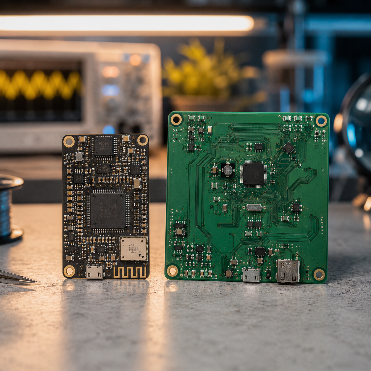
> $50,000
Typical all-in cost of a single PCB respin — fabrication, assembly, expedited parts, debug time, and slipped schedule. Defect cost rises roughly 10× for each stage it survives.
Source: industry TCO analysis (Quilter.ai, 2026) & DFM cost-of-failure rule of thumb; U.S. Bureau of Labor Statistics May-2024 median engineer wage $111,910–$127,590. Figures are industry-reported ranges, not a PCBark-specific guarantee.
The escalation buyers underrate is a real trade-off: moving a board from IPC Class 2 to Class 3 adds roughly 15–40% to fab and assembly cost, worth it for medical and high-vibration designs, wasteful for a consumer sensor. The respin that a proper DFM review prevents costs more than the entire Class-3 premium. As one engineer summarised after paying double at a second vendor: “the assembly was double the price at PCBWay, but PCBWay saved me from making faulty boards.” Paying for design scrutiny is cheaper than paying for the respin it prevents.
From Prototype to Volume, Procurement, Lead Times & Sourcing







IoT PCB Engineering & Cost Estimation Tools
IoT Board Stack-Up Estimator
Match your device class + connectivity to a realistic board build before you request a quote.
Access Tool
Wireless Protocol Design-Constraint Lookup
Each IoT radio imposes its own board rules. Pick a protocol to see the constraints PCBark designs to.
Access Tool
IoT PCB Cost-Driver & Landed-Cost Estimator
See which factors move your IoT board quote — and the hidden costs unit price hides. No fake dollar figures.
Access Tool