SMT Assembly

SMT Assembly Services, Surface-Mount PCB Assembly, Proto to Production

Factory-direct surface-mount assembly across 8 SMT lines and 9 million placements per day, from a single 0201 passive to a 1,000-ball BGA, built to IPC-A-610 Class 2/3 and verified with in-house AOI, 3D X-ray, ICT and functional test.

ISO 9001:2015 IPC-A-610 Class 2/3 J-STD-001 16+ years 8 SMT lines 9M placements/day
SMT Assembly Lines and Production
8
SMT lines
9M/day
Placements
0201–BGA
Component range
680×550mm
Max board
Class 2/3
IPC-A-610
1–15 days
Turn time
What SMT Assembly Solves: From Bare Board to Tested PCBA

SMT assembly is the automated process of assembling electronic components, printing solder paste, placing surface-mount parts, and reflow soldering them directly onto the surface of a printed circuit board to produce a finished, tested PCBA. It replaced through-hole as the dominant assembly technology behind more than 90% of modern electronics because it puts 100+ components per square inch where through-hole fits roughly 20, and because a single reflow forms every joint at once. (USPTO US11825606B2) What’s hard isn’t the definition, it’s getting consistent, inspectable joints on a board that mixes a 0201 chip resistor with a hidden-ball BGA, on time, at a price that survives the customs line.

Why this page is data-first

Most SMT assembly pages publish a capability list and a “high quality” promise. This page publishes the line count, the placement rate, the component floor, the inspection stack, the workmanship class, and the landed-cost math, because those are the things a procurement manager and a hardware engineer actually compare. Where a figure is an industry-typical range rather than our measured spec, we say so.

Every buyer we quote is really weighing the same five risks: fine-pitch and BGA yield, a capacity ceiling that stalls your ramp, an opaque quote that balloons after freight and tariffs, quality that drifts batch to batch, and an overseas factory that builds what it thinks the drawing says. This page answers each with the numbers behind our lines, not adjectives, and reads as a practical guide to surface mount technology for buyers rather than a textbook. Our turnkey PCB assembly services run end to end, from PCB manufacturing and component sourcing through surface mount assembly, through-hole assembly and functional test, so manufacture and assembly happen under one roof.

The SMT Assembly Process: Solder-Paste-to-AOI 6-Stage Process Map

An SMT assembly process is only as reliable as its weakest stage, so each of the six stages on our lines is metrology-gated before the board advances. It starts when the printing process lays paste on every pcb pad and the SMT pick and place stage seats the parts; the reflow soldering process then forms all joints in a single thermal pass.

The reflow profile is where most yield is won or lost: lead-free SAC305 melts at 217–220°C , about 34°C hotter than the old tin-lead eutectic, so the oven has to drive a peak of 230–250°C with a ramp under 3°C per second and 30–90 seconds above liquidus to wet the joint without cooking the part. That tight window is exactly why the SMT process is run as a closed loop, a topology recent EMS patents formalize as a self-correcting print, SPI–place, AOI–reflow line.

USPTO US20240248463A1, Jabil, 2024

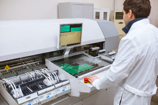
Pick-and-place stage of the SMT assembly process seating surface-mount components onto a printed circuit board
The pick-and-place stage of the SMT assembly process, components seated on a PCB before reflow.
No. Stage What happens In-line control
1 Solder paste printing Stencil deposits paste on pads Aperture / area-ratio controlled stencil
2 SPI (paste inspection) Volume / height / offset of every deposit 3D SPI before any part lands
3 Pick-and-place Components placed onto the PCB 0.15 sec/chip, 0.7 sec/QFP
4 Reflow soldering Single thermal pass forms all joints SAC305 peak 230–250°C, TAL 30–90s
5 AOI Automated optical inspection of every joint Line-speed 3D AOI
6 3D X-ray + test Hidden BGA joints + electrical verification X-ray, ICT, flying probe, function test

Moisture discipline you rarely see published

Before any moisture-sensitive part or BGA sees 230°C, it’s handled to J-STD-033. IPC/JEDEC J-STD-033, NSWC Crane An MSL-3 part has a 168-hour floor life at the bench; exceed it and it gets a 24-hour bake at 125°C to reset the clock, with a hard ceiling of three reflow passes per component. Skipping that step is how you get popcorning under a BGA that no amount of profile tuning will fix.

Unlike a shop that runs one generic profile for every board, the reflow process here’s tuned per assembly, because the common mistake (too hot and the part cooks, too cold and the joint never wet) is what turns a clean placement into a field failure.

Each pick-and-place machine is calibrated for component placement down to 0201, and the reflow oven is profiled against the board’s thermal mass rather than a default recipe. That disciplined pcb assembly process is the manufacturing process that separates a repeatable line from a one-off, and it captures the searches engineers actually run, smt process, reflow soldering, and smt stencil design.

PCBark SMT Assembly Capabilities: The 9-Million-Placement Capacity Ladder

Capacity is the spec the rest of the SERP hides, capability lists rarely state a daily placement number, so a buyer can’t tell whether a ramp will fit. Here it’s, unhidden: 8 surface-mount lines, 9 million placements per day, a 0.15-second chip cycle, and a component window from a 0201 passive up to fine-pitch BGA, QFP, CSP and long connectors. Placement registration for that fine-pitch work is the kind of problem recent tooling patents target with topography-matched chucks. (WIPO WO2023056072A1, 2023)

Capability PCBark spec
SMT lines 8 lines
Placement capacity 9,000,000 placements / day
Placement speed 0.15 sec/chip, 0.7 sec/QFP
Component range 0201 / 01005-class · CSP · BGA / µBGA · QFP / QFN / PLCC · long connector
Max board size 680 × 550 mm (smallest 0.25 × 0.25 in)
Sided Single- and double-sided SMT + mixed SMT/through-hole
Wave / selective solder Max PCB width 450 mm; component height top 120 mm / bottom 15 mm
Press-fit 0–50 kN, max board 800 × 600 mm
Solder & paste Leaded and lead-free; water-soluble paste
File formats BOM, Gerber, Pick-and-Place (XYRS)

Honest Capacity & BOM Integrity

A capacity ladder only matters if the small end is honest. A common buyer pain is that unapproved component substitution ships non-compliant parts the buyer never approved, forcing a production stop. PCBark holds the BOM you signed off, turnkey, partial-turnkey, or consignment, and surfaces any substitution as a documented engineering query, not a silent swap.
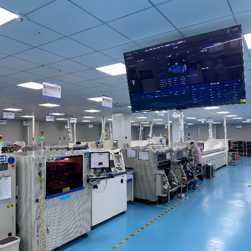
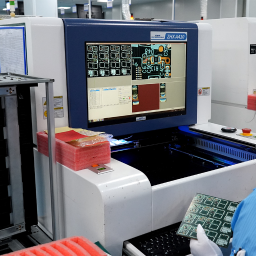
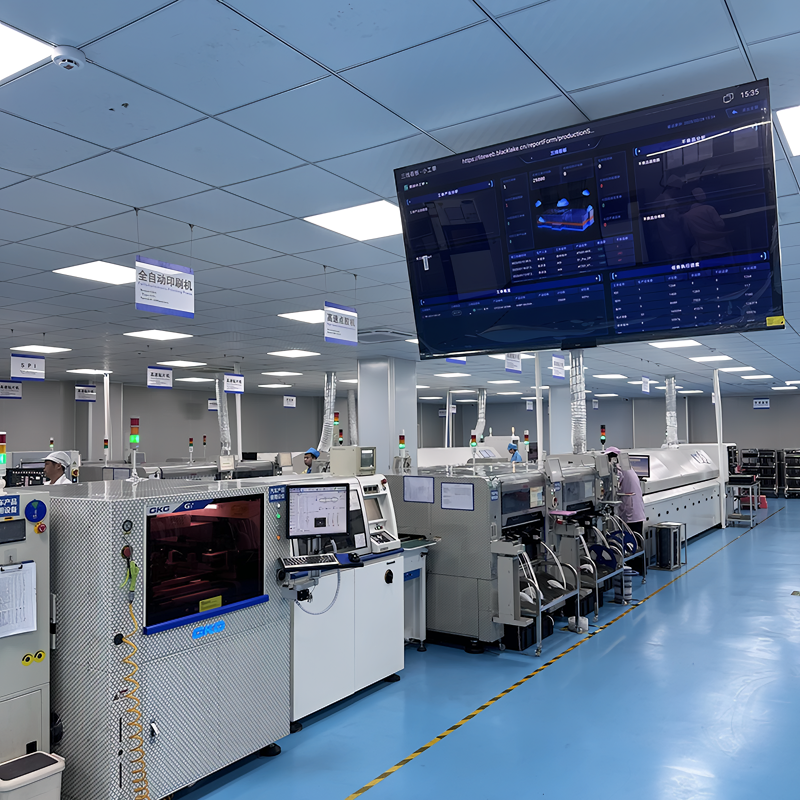
PCBark SMT assembly floor with multiple surface-mount lines and real-time line monitoring

PCBark SMT assembly floor with multiple surface-mount lines and real-time line monitoring
PCBark SMT assembly floor, multiple surface-mount lines under real-time line monitoring.

Those same lines place SMT components and fine-pitch smt parts that handle smt manufacturing at volume, running prototype PCB assembly, smt pcb assembly and double sided smt assembly without re-tooling the floor. Clean surface mount pcb assembly starts upstream at pcb design, a manufacturable footprint on a sound surface mount pcb, so our DFM read covers the board and the parts together. Mixed work finishes on a wave soldering process or selective solder, and for high-mix electronics manufacturing the same manufacturing capabilities build a single board or thousands of identical pcb assemblies.

Get a free DFM review

The SMT-vs-Through-Hole Decision Grid: When to Use Each

The reflex assumption is that surface mount always beats through-hole, and for density and high-frequency work it does, but that isn’t the whole grid. Through-hole still wins on mechanical strength and field repair, which is why the right answer is a mix, not a religion.

A Chinese-origin process patent quantifies the headline gap: SMT cuts board size 40–60%, weight 60–80% and assembly cost 30–50% versus through-hole at volume.
USPTO US11825606B2, 2023
Ranges in the table below are industry-typical for a smt vs through hole decision, not single measured points.

Dimension SMT Through-hole
Component density 100+ / sq-in, down to 0201 ~20 / sq-in
Board area used 50–80% less Baseline
Placement Automated, ~0.15 s/chip Manual / semi-auto insertion
High-frequency Lead inductance <1 nH; good to 1 GHz+ ~5–15 nH/lead; degrades >10 MHz
Mechanical strength Surface fillet only Through-board anchoring (best for shock/vibration)
Cost crossover Cheaper above ~100–500 units Cheaper for <50–100 unit prototypes
Best for Dense, high-volume, RF, miniaturized Power, connectors, high-vibration, field-serviced

Environmental Trade-Offs

There’s a second, costlier assumption hiding here: that going lead-free is purely an upgrade. It isn’t. A small amount of lead is actually the strongest defense against tin-whisker failure, and lead-free’s higher melt point permanently shrinks the reflow window, so for harsh-environment builds the alloy choice is a deliberate trade-off, not a default.

Engineering Judgment in Manufacturing

In our own factory the same calibrated lines run both surface mounting and through-hole technology, so the choice is engineering judgment, not a sales limit. The surface mount technology advantages, density, automation and high-frequency performance, make it the default for most designs; the advantages of SMT are decisive there, yet traditional through-hole technology still earns its place on power and high-vibration boards, where conventional assembly or through-hole pcb assembly survives insertion force and shock. PCBark makes that call with you up front rather than after the first thermal-cycle failure.

Quality & Full Test Stack

The most expensive assumption a buyer makes is that an X-ray machine means the board is verified. It doesn’t. Hidden BGA joints can’t be visually inspected after reflow, X-ray proves a ball is physically connected, but it can’t tell you the joint is electrically or structurally sound, and AOI alone never sees under the package at all. That’s why our stack pairs imaging with electrical test: AOI and 3D X-ray for structural and hidden-joint defects, then ICT, flying probe, burn-in and functional test for the rest. Dedicated X-ray inspection of hidden solder joints is now its own patented discipline. (EPO EP4134883B1)

Workmanship is held to a stated class, not a slogan. IPC-A-610 and its companion process standard J-STD-001 tighten measurably from Class 2 to Class 3, and the difference is where harsh-environment reliability lives.

“We treat AOI and X-ray as different questions, not redundant ones. AOI catches the visible defect rate on every joint at line speed; the 3D X-ray exists for the joints you physically cannot see. A board that passes one but not the other never ships as good.”
// PCBark Engineering Team

Acceptance Criterion Matrix

Parameter Class 2 (Industrial) Class 3 (Hi-Rel)
Side overhang, max≤50% of lead width≤25% of lead width
Toe width, min≥50% of lead width≥75% of lead width
Side fillet~75%~100%
BGA voidingWider allowance≤9–25% tightly held
Typical applicationInstrumentationAerospace, Medical, Auto

System Certifications

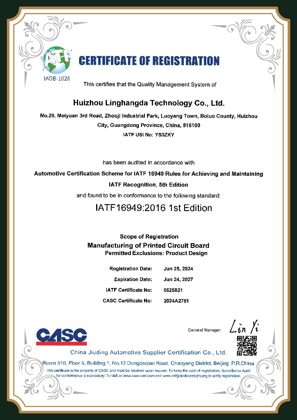
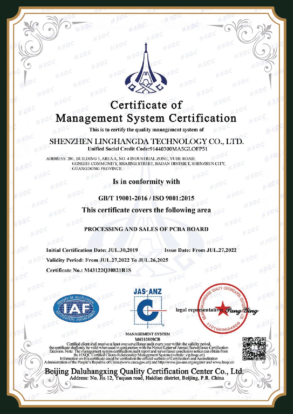
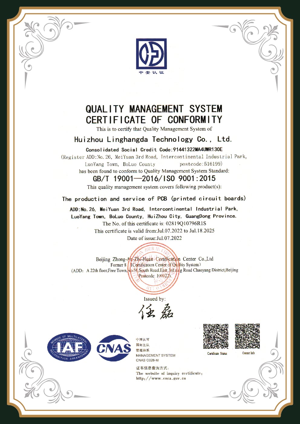
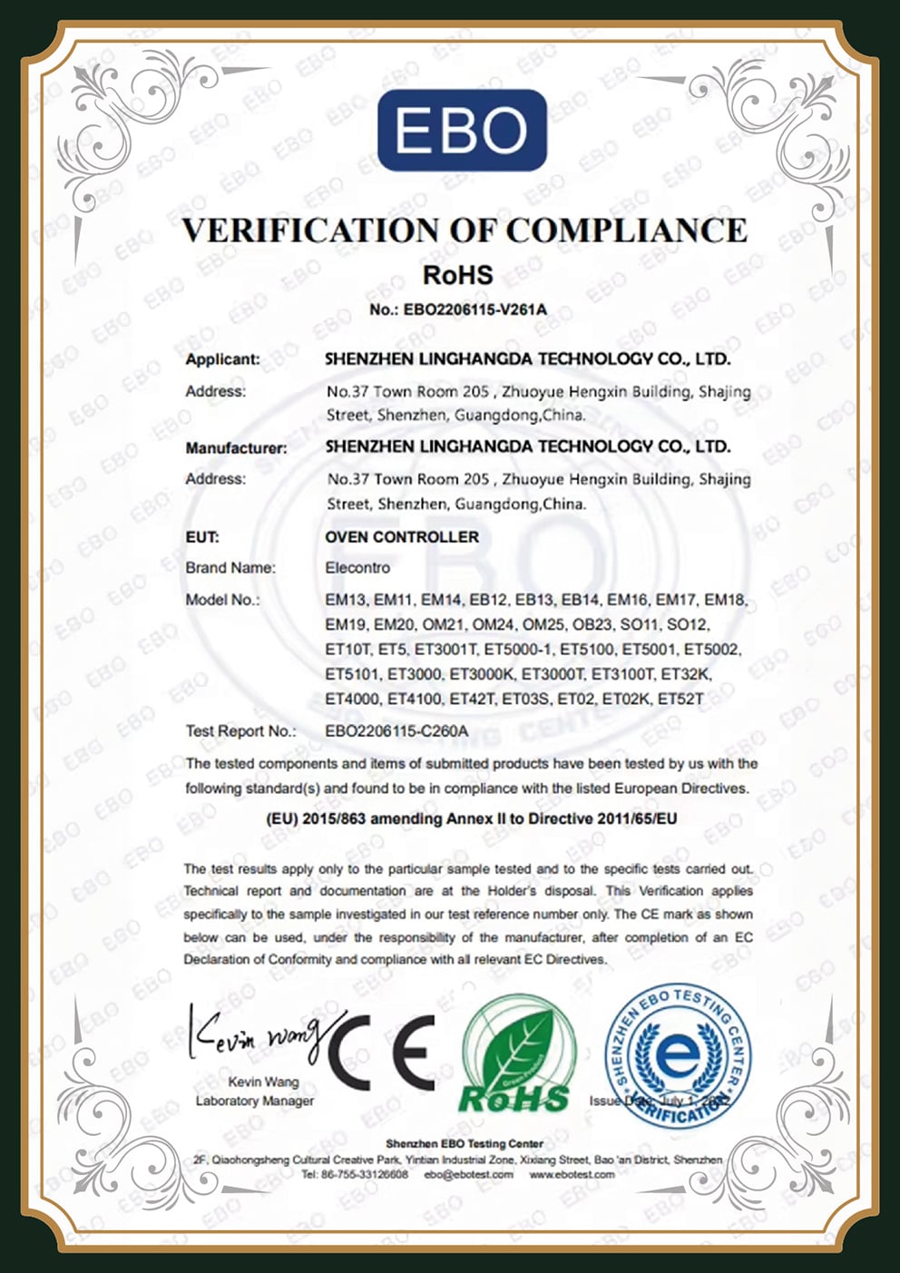
ISO 9001:2015

Quality Sys

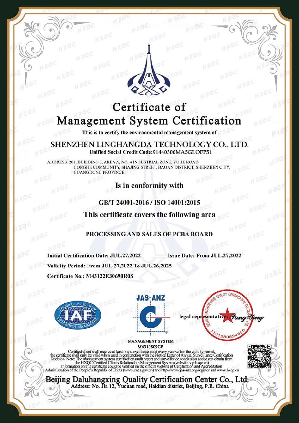
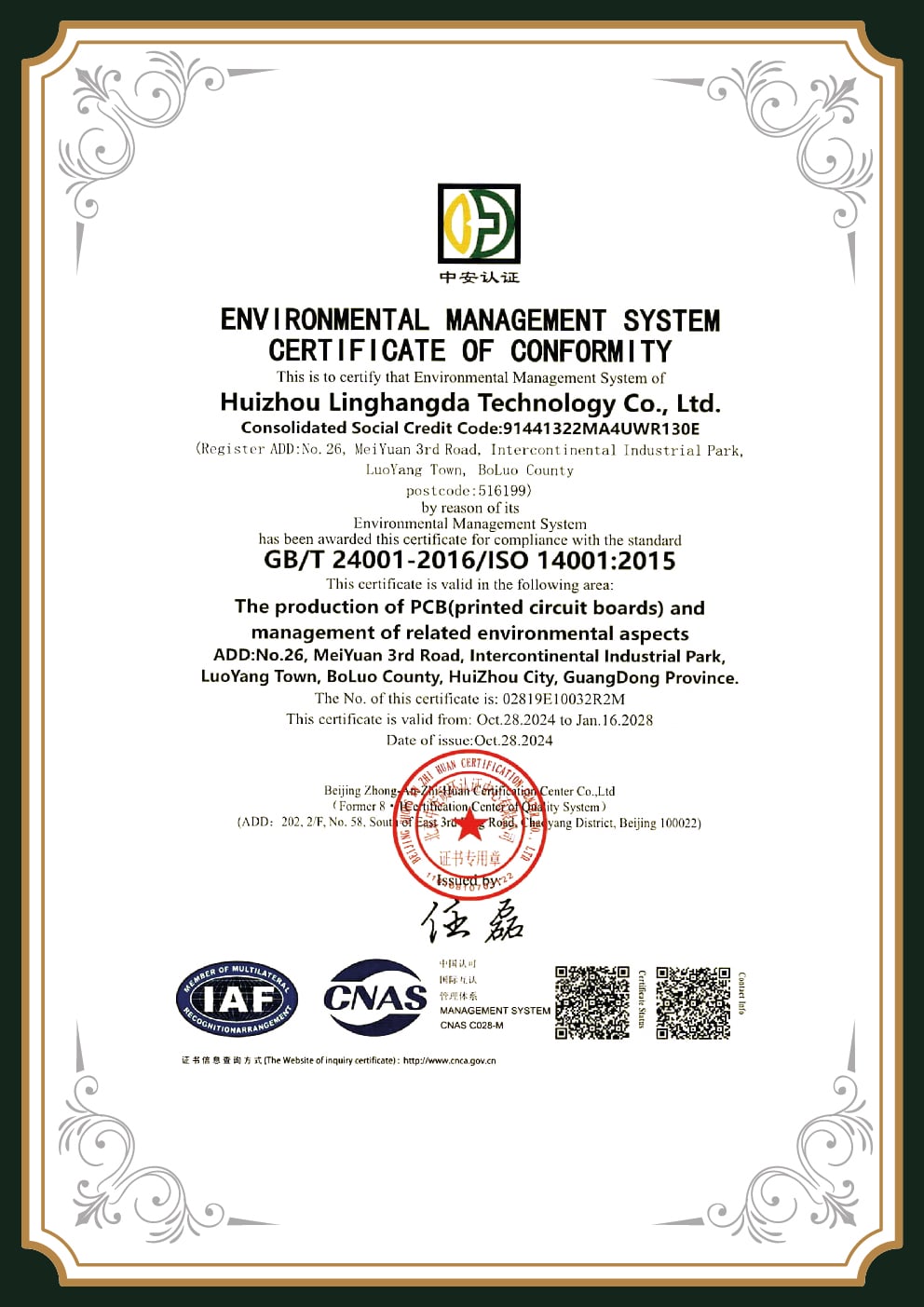
ISO 14001

Environmental

IPC-A-610 Cl 3

Acceptance

J-STD-001

Soldering

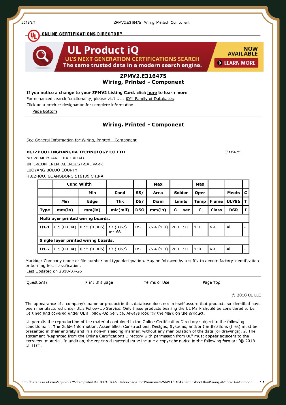
UL · RoHS

Compliance

REACH

Substance
This is where a supplier earns trust: buyers screen on a certified quality system, a stated IPC class, and inspection coverage matched to board complexity. The standards reference for class definitions is published by IPC itself.
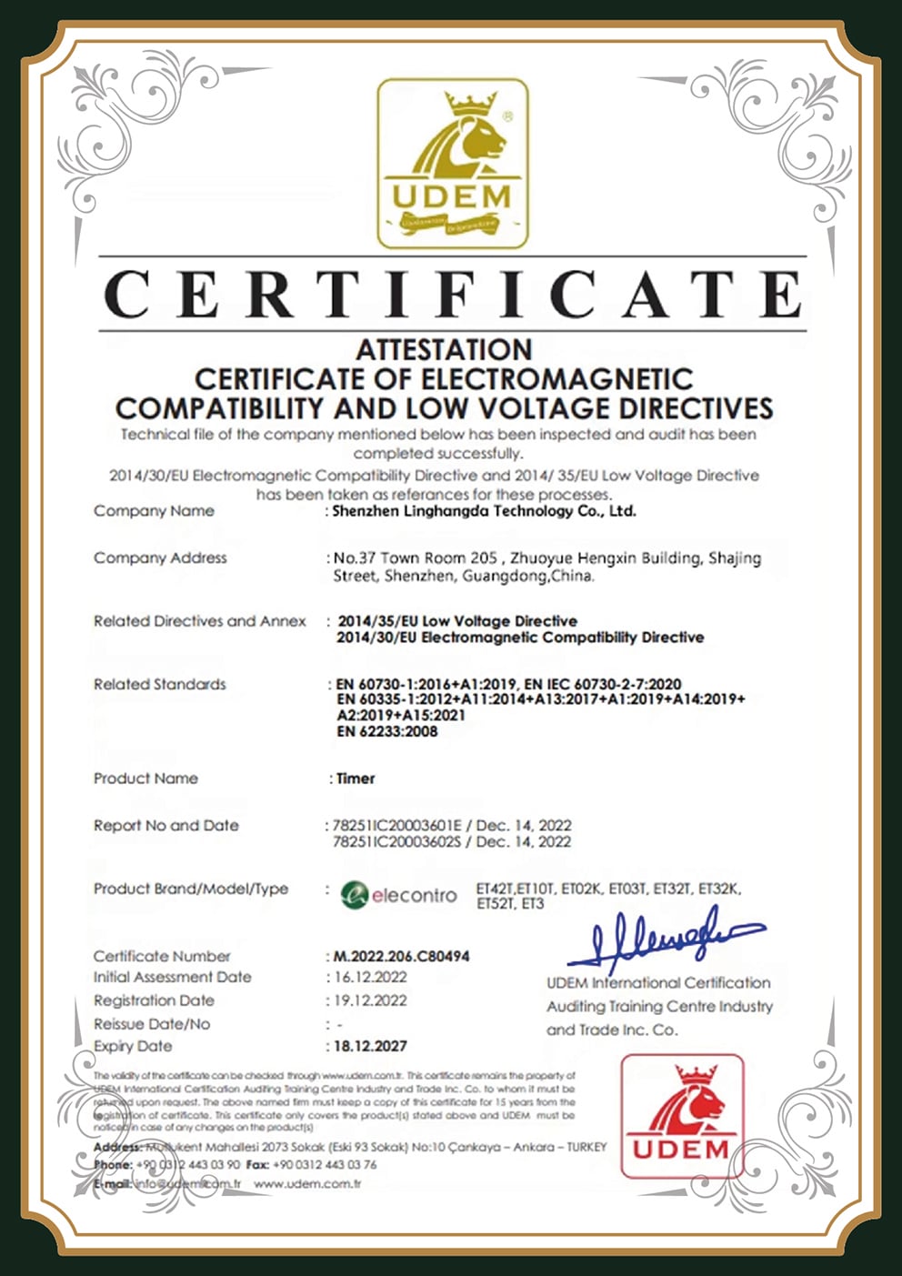
× Zoomed Certification

SMT Assembly Costs & Lead Times: The 5-Lever SMT Cost Model

A language barrier turn drawings into defects, and a headline turn time hides the real delivery date, the two cost surprises buyers report most. PCBark answers both with transparency instead of a single magic number, because an SMT assembly quote is driven by five levers, and the landed cost from China carries adders that an ex-works price never shows. Modeling that honestly is the core 2026 sourcing decision: relocating assembly alone doesn’t guarantee duty relief.

Factory-Direct vs US-EMS vs Broker, landed-cost crosswalk

The honest comparison isn’t unit price; it’s total landed cost. China-origin PCBs and PCBAs carry a 25% additional Section 301 tariff on top of the (often free) base duty unless a valid exclusion applies. (USTR, Section 301) The $800 de-minimis exemption has also been suspended, so even prototype shipments now need formal entry. (Executive Order 14324)

+45%

One buyer’s real China-to-US PCBA order ran about 45% over the ex-works quote once shipping, taxes and tariffs were added. Compare landed cost, not unit price.
Landed Cost Breakdown Data

Industry/buyer-reported figure; 178 Section 301 exclusions run to Nov 10, 2026, and duty drawback can recover up to 99% of eligible duties on re-exported goods.

The five cost levers

01

BOM & placements

Unique line items and total placements drive machine time and sourcing labor
02

NRE & tooling

Stencil and program are one-time; they dominate small runs
03

Density & class

Fine-pitch/BGA and IPC Class 3 add stencil precision, X-ray and inspection labor
04

Volume & turn

Setup spreads over units; quick-turn carries a rush premium
05

Landed-cost adders

Section 301 tariff + freight + customs/broker on top of ex-works

Choosing a partner on unit price alone understates true total cost of ownership by roughly 20–30% once capital, logistics, duties and risk are counted, which is why a factory-direct EMS with in-house test depth usually beats both a broker (who marks up and controls nothing) and a domestic shop quoting 4–5× the unit price. To start a quote we need only your BOM, Gerber and Pick-and-Place files; pricing for your smt assembly service follows from the five levers above. Request a landed-cost estimate and we’ll model it against your volume and destination.

SMT Assembly Planning & Evaluation Tools

SMT Landed-Cost Crosswalk

Compare the landed cost of a China-direct SMT build — not the headline unit price. Section 301 tariff, freight and broker fees included.

Evaluate Costs

SMT vs Through-Hole Selector

Five questions map your board onto the right assembly technology. Most real designs are mixed — this tells you where the balance sits.

Select Technology

SMT Complexity & Lead-Time Estimator

A quick read on where your build sits on the complexity scale and which lever drives its lead time. Not a quote — a planning aid.

Estimate Lead Time

FAQ: SMT Assembly Services

Find answers to the most common questions about our Surface-Mount Technology assembly processes, quality standards, and capabilities.

What is the difference between SMT and SMD assembly?

SMT (surface-mount technology) is the assembly process — printing paste, placing parts and reflow soldering. SMD (surface-mount device) is the component that process places. In short: SMT is how, SMD is what. You will see both terms on the same job.

What does SMT stand for?

Surface-Mount Technology — the method of mounting electronic components directly onto the surface of a PCB rather than through drilled holes.

Can a board mix SMT and through-hole components?

Yes. Most real designs are mixed-technology. We run surface-mount, then through-hole via wave, selective or hand soldering, with one BOM and one inspection plan covering both.

Do you handle low-volume and prototype assemblies?

Yes — 1–10 piece prototypes through 1,000+ piece production run on the same calibrated lines, typically 1–5 working days for a prototype once files and materials are confirmed.

What files do you need to start an SMT quote?

A Bill of Materials (BOM), Gerber files, and a Pick-and-Place / centroid file (XYRS). Those three let us run DFM, source components and program the line.

What industry standards ensure quality in SMT assembly?

IPC-A-610 sets visual acceptance (Class 2 or Class 3), J-STD-001 governs the soldering process, and J-STD-033 controls moisture-sensitive and BGA handling. We build to the class your application requires under an ISO 9001:2015 system.

What inspection and testing do you use?

3D SPI verifies solder-paste volume after printing, AOI inspects every joint after placement and reflow, and 3D X-ray looks under BGA and QFN packages for hidden voids, bridging and head-in-pillow that no camera can see. Electrical coverage follows with ICT, flying probe, burn-in and functional test as the board demands. X-ray proves a joint is connected; electrical test proves it actually works — so high-reliability boards get both, never one as a substitute for the other.

How much does SMT assembly cost?

It is driven by the five levers above — BOM and placements, NRE/tooling, density and IPC class, volume and turn, plus landed-cost adders like the 25% Section 301 tariff. Send your BOM/Gerber/Pick-and-Place and we will model a transparent quote rather than a placeholder number.

Do PCBs need cleaning after SMT assembly?

It depends on the flux and the end-use class. No-clean processes are common for Class 2; water-soluble paste and high-reliability Class 3 builds are cleaned and verified. We match the cleaning step to the solder chemistry and the standard.

Get an SMT Assembly Quote

Send your BOM, Gerber and Pick-and-Place files. PCBark will run DFM, model your landed cost, and quote 0201-to-BGA surface-mount assembly built to your IPC class.

Get an SMT Assembly Quote