Get in touch with PCBark Company

⚙️ IPC-A-610 Certified / Class 2 & 3
PCB Assembly
PCB Assembly Services From a Full-Turnkey Manufacturer
Nine assembly services in one coordinated workflow, with offshore cost advantages and inspection controls built for U.S. and global buyers. SMT, through-hole, BGA and box build are quoted with the landed-cost assumptions shown before you order.
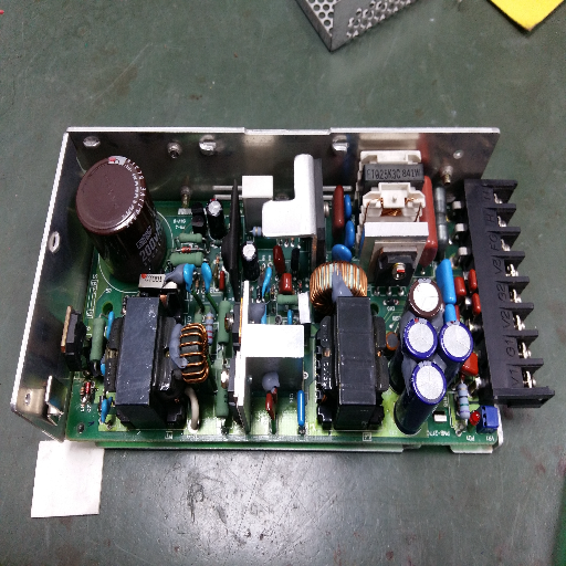
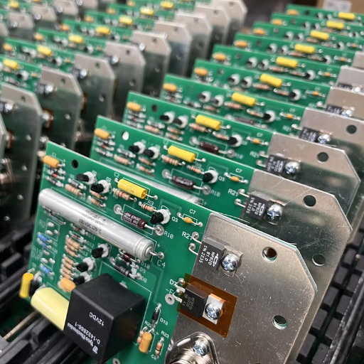
PCB assembly is the process of populating a bare printed circuit board with electronic components: solder paste printing, surface-mount placement, reflow, through-hole insertion, soldering, inspection and test. PCBark runs the full sequence in-house on 8 SMT lines, with DFM review, component sourcing, inspection and testing coordinated under one quote.
8
SMT lines (Yamaha YSM)
9M
placements / day
0201→BGA
component range
680×550 mm
max board size
1–15 days
turn time
Class 2 / 3
IPC-A-610 workmanship
SMT+THT+Box
build types
16 yrs
since 2010
Process Overview
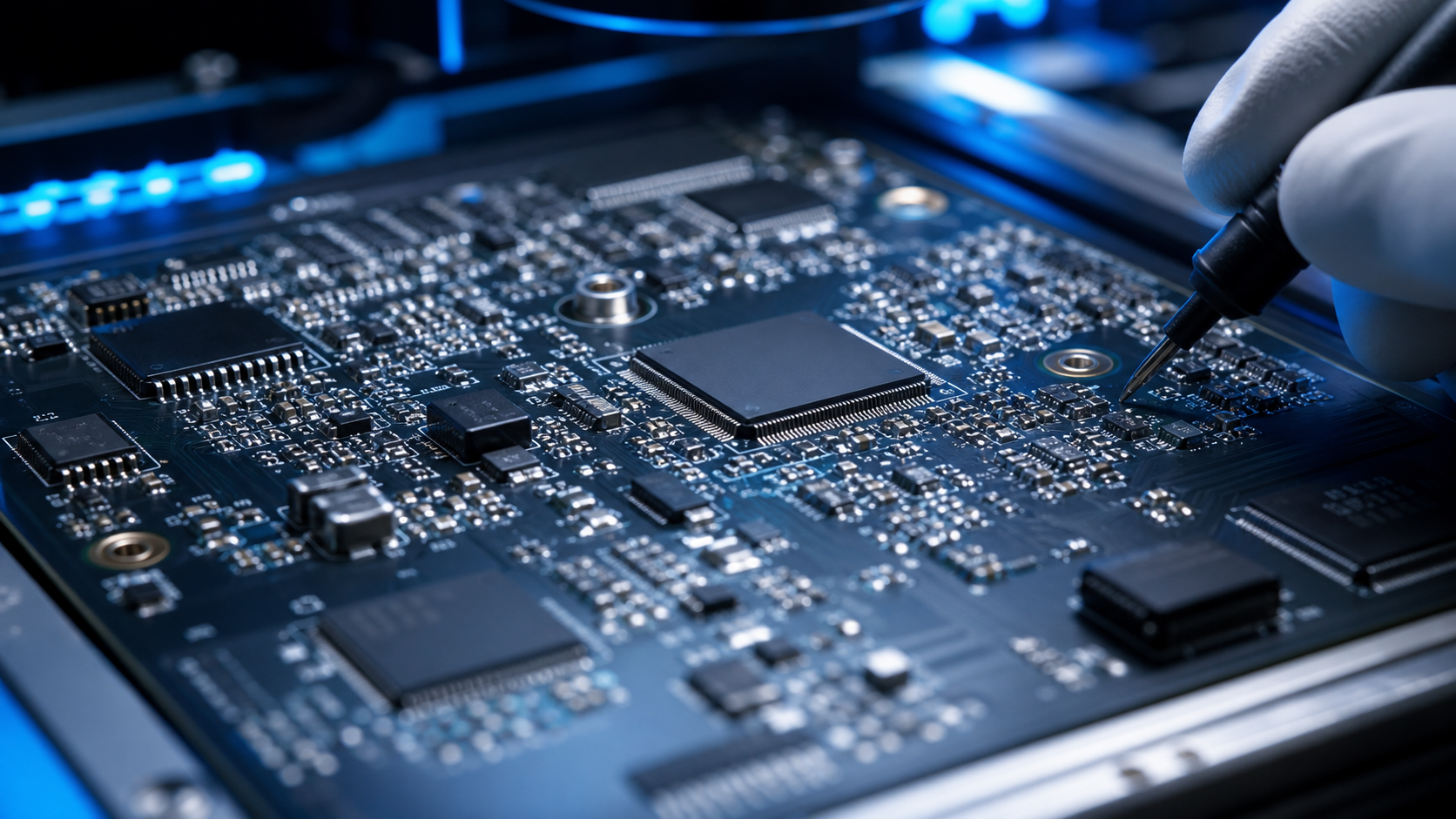
What PCB Assembly Is — and Why It Comes Down to Field-Failure Risk
The Reality of Offshore Disappointment
A finished printed circuit board assembly only matters if it still works after shipment. The real risk is rarely the first quote; it is the failure that appears months later in the field.
That concern is valid: counterfeit components sourced through grey channels can pass an initial power-up and then fail in service, and PCB assemblies inspected only by sampling can carry hidden solder defects into a customer’s hands.
Transparency and Inspection Discipline
Reliability is not decided by the country label alone; it comes from sourcing control, process traceability and inspection discipline. A standard commercial assembly can be built offshore successfully when the supplier documents component sources, verifies solder quality and gives engineering access to the people reviewing the job. Problems usually come from opaque economy flows where substitutions, rework and inspection limits are not visible before shipment.
The PCBark Standard
PCBark closes that gap with documented data review, layered inspection and a single engineering contact for RFQ and production questions. The goal is straightforward: give purchasing a quote they can compare and give engineering enough detail to judge risk before the board ships. PCBark has delivered PCB assembly and testing as core manufacturing services since 2010.
Closed-Loop SMT Process Control
Because solder paste printing drives many SMT defects, PCBark gates that step first with 3D solder-paste inspection before placement. The control loop is practical: print, inspect, place, inspect, reflow and feed deviations back to the process team. For fine-pitch and BGA work, AOI and X-ray checks add coverage before electrical or functional test requirements are applied.
9 PCB Assembly Services Under One Roof
Most buyers don’t need one assembly process, they need whichever combination their board demands, plus a partner who can carry the same project from a 5-piece prototype to a 50,000-unit production run of finished PCB assemblies without re-sourcing. From a small-volume prototype to production, one printed circuit board assembly services partner keeps every PCB project on the same line, traditional PCB assembly and advanced packaging together, instead of handing your PCB boards down a chain of separate vendors.
Big contract manufacturers shun low-volume and custom work; PCBark treats the full range as one continuous capability. The Coverage Atlas below maps every service we run, what it’s for, and where it fits your volume, so you can route your board to the right process in one read.
PCB Assembly Coverage Atlas
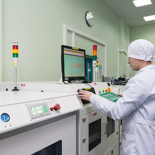
Turnkey PCB Assembly
- What it is Fab + component sourcing + assembly + test, single PO
- Best for Buyers who want one accountable partner
- Volume Proto → high volume
- Key spec BOM + Gerber in, tested board out
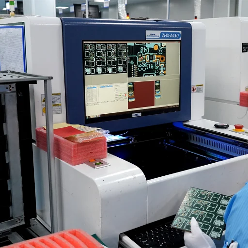
SMT Assembly
- What it is Surface-mount placement + reflow
- Best for Modern high-density boards
- Volume All volumes
- Key spec 0201 to fine-pitch BGA/QFN
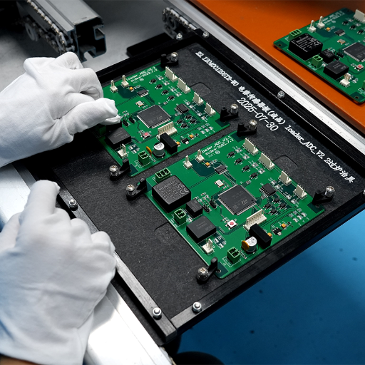
Through-Hole / DIP Assembly
- What it is Leaded parts, wave / selective / hand solder
- Best for Connectors, power, high-reliability joints
- Volume All volumes
- Key spec Wave width to 450 mm
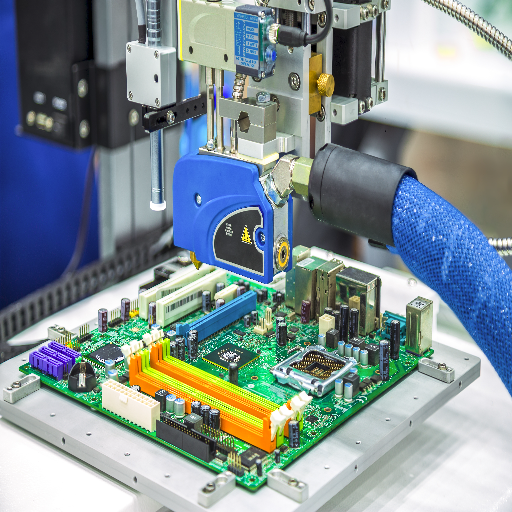
BGA Assembly
- What it is Ball-grid-array placement + 100% X-ray
- Best for Processors, FPGAs, dense ICs
- Volume Proto → volume
- Key spec 3D X-ray on every hidden joint
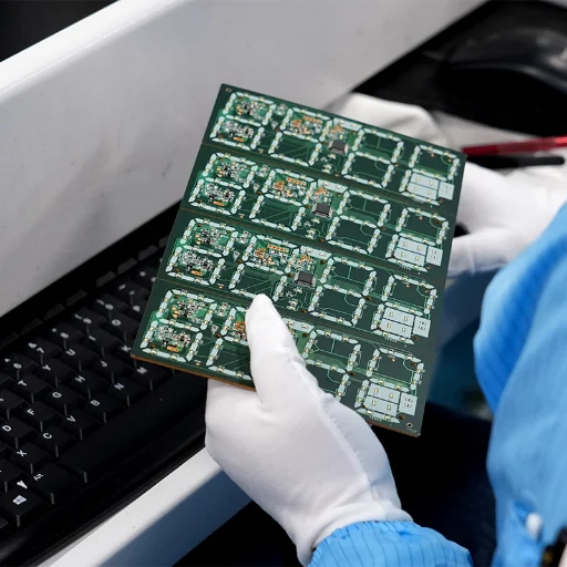
Prototype PCB Assembly
- What it is Fast first builds, flying-probe test
- Best for Design validation, NPI
- Volume 1–50 pcs
- Key spec 24–72 h quick-turn available
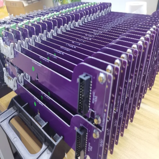
Quick-Turn / Fast PCB Assembly
- What it is Expedited build + ship
- Best for Missed-deadline recovery
- Volume 1–500 pcs
- Key spec 24 h expedited (1–10 pcs)
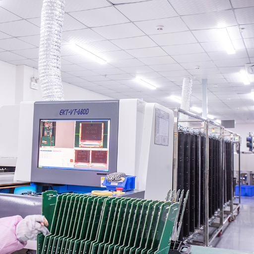
Low-Volume PCB Assembly
- What it is Short runs without volume penalty
- Best for Niche / industrial products
- Volume 10–1,000 pcs
- Key spec No re-source moving to volume
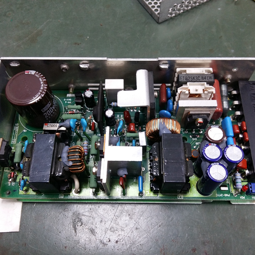
Box Build / Final Assembly
- What it is Enclosure, cabling, system integration, FCT
- Best for Finished sub-assemblies
- Volume Proto → volume
- Key spec Cabling + cable assembly + test
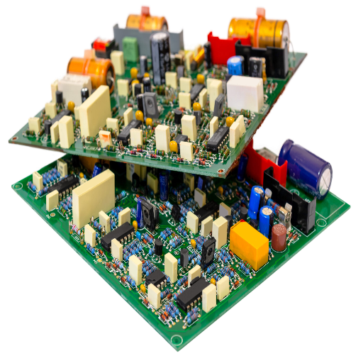
Circuit Card Assembly (CCA)
- What it is Class 3 workmanship, ruggedized builds
- Best for Industrial / high-reliability
- Volume All volumes
- Key spec IPC-A-610 Class 3 — see honest scope below
That breadth is exactly what buyers say keeps them with a full-service house: cheaper regional shops lose the work because they can’t match the range of thicknesses, finishes, package types and on-hand parts. Whether you need pcb assembly services for a single dense board, custom pcb assembly for a one-off design, or a long-term pcb assembly manufacturer for full turnkey pcb assembly across a product line, the line, the inspection stack and the engineer stay the same.
Assembly-Type Routing Path
If your board carries surface-mount components only, route it to SMT Assembly, and add 3D X-ray when it includes BGA or QFN packages.
If you mix SMT with leaded parts or connectors, combine SMT with Through-Hole and selective soldering on the leaded side.
If you need boards this week to hit a deadline, start with Quick-Turn or Prototype assembly.
If you want one PO for board, parts and build, choose Turnkey PCB Assembly, or pair it with our PCB manufacturing for fab-and-assembly in one place.
If you’re shipping a finished product with an enclosure or cabling, move to Box Build / Final Assembly.
PCB Assembly Capabilities, Package Limits and Inspection Process

Engineering
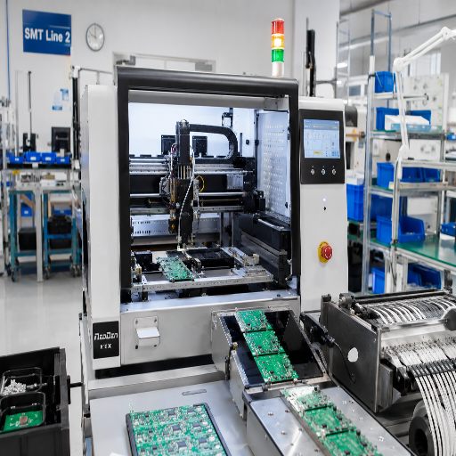
Engineers don’t want adjectives; they want limits. These are the numbers our floor runs to on real PCB assemblies, drawn from our own equipment list, eight surface-mount lines built on Yamaha YSM placement platforms, GKG and ZhenHua printers, JingTuo reflow ovens and a Nitto wave solder system.
SMT lines8 lines
Placement capacity9,000,000 placements / day
Placement speed0.15 sec / chip · 0.7 sec / QFP
Smallest passive0201 (metric 0603)
Package supportBGA, micro-BGA, QFN/leadless, CSP, QFP, long connectors
Max board size (SMT)680 × 550 mm · smallest 0.25″ × 0.25″
Wave solderMax PCB width 450 mm
Press-fit range0–50 kN · max board 800 × 600 mm
Solder typesLeaded, lead-free, water-soluble paste
Build typesSMT, through-hole, mixed, box build
Turn time1–15 days
From Bare Board to Tested PCB Assembly — the Build Flow
Every PCB assembly process on our floor follows the same disciplined sequence, whether it ends as a 5-piece prototype or a production lot of finished PCB assemblies. It opens with a PCB design and data review, Gerber, ODB++ or IPC-2581 plus the BOM, then solder paste printing onto the bare board through a laser-cut stencil, checked by SPI before a single part lands.
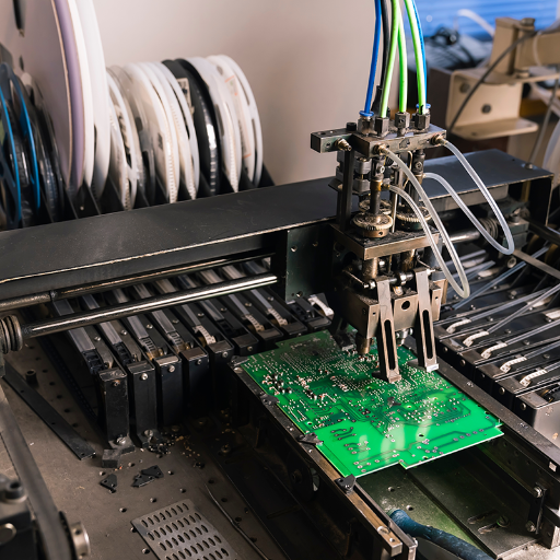
Our pick-and-place machines handle component placement for the SMT parts and surface mount devices, from 0201 passives, tiny parts smaller than a grain of rice, to fine-pitch BGAs, before each board passes through the reflow oven. Boards carrying through-hole components (PTH) move to wave soldering or selective soldering, or are soldered by hand for the lowest volumes, and mixed assembly boards (SMT plus thru-hole components) get both.
After cleaning, we add the finishing steps required by the application: conformal coating when moisture or chemical exposure is a risk, requested markings, and box build assembly into enclosures or cabling. Each step is documented and traceable, so the PCBA process turns bare copper and laminate into working boards under one manufacturing flow instead of a black box.
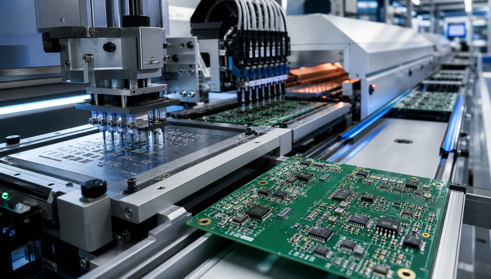
Layered PCBA Inspection Checkpoints
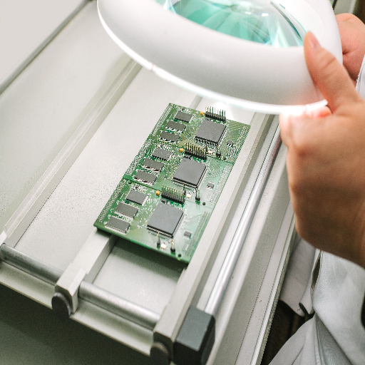
No single test proves that a board works in every condition. AOI verifies what the camera can see, but it cannot inspect hidden BGA solder joints. PCBark uses layered checkpoints so each method covers a different defect class: SPI for paste, AOI for placement and visible solder, X-ray for BGA and hidden joints, plus ICT and functional testing when the project requires electrical proof before shipment.
| No. | Checkpoint | Catches | Blind to | When we run it |
|---|---|---|---|---|
| No.1 | SPI (3D solder-paste inspection) | Paste volume, bridging, insufficient deposit | Placement / electrical | Before placement (≈80% of defects start here) |
| No.2 | AOI (automated optical inspection) | Missing/misaligned parts, visible solder defects | Hidden joints, electrical | After reflow |
| No.3 | AXI / 3D X-ray | Solder voids, BGA/QFN shorts & opens | Electrical function | All hidden-joint boards |
| No.4 | ICT (in-circuit, bed-of-nails) | Shorts, opens, wrong/missing values | System behaviour | Volume runs |
| No.5 | Flying probe | Same electrical checks, no fixture | System behaviour | Prototype / low volume |
| No.6 | Functional test + burn-in | Real-world operation, infant mortality | — | On request / Class 3 |
This stack is built on established metrology, high-speed X-ray inspection is itself a patented field (see US Patent US9129715B2, high-speed X-ray inspection microscope). It also defines our honest capability line. Standard SMT, through-hole and mixed boards run clean. Where buyers report offshore trouble, and where we ask for an upfront conversation, are the hard cases: Cheap economy assembly shorted the connector pins under the metal body on a USB-C part for one forum buyer, a failure the correct (not the cheapest) process avoids. We quote the right process for the board, not the cheapest one that books the order. Every circuit assembly we build to IPC Class 3 gets 100% automatic optical inspection plus X-ray, and the testing and inspection records travel with the boards, the added manufacturing costs of that rigor are exactly what a Class 2 build lets you skip when the application allows.
We do not let a board with hidden BGA joints leave the floor on AOI alone. If the camera can’t see the joint, the X-ray does, and on a Class 3 build, that is 100% of those joints, not a sample.
Want the full numbers on your packages?
Download PCBA Datasheet_
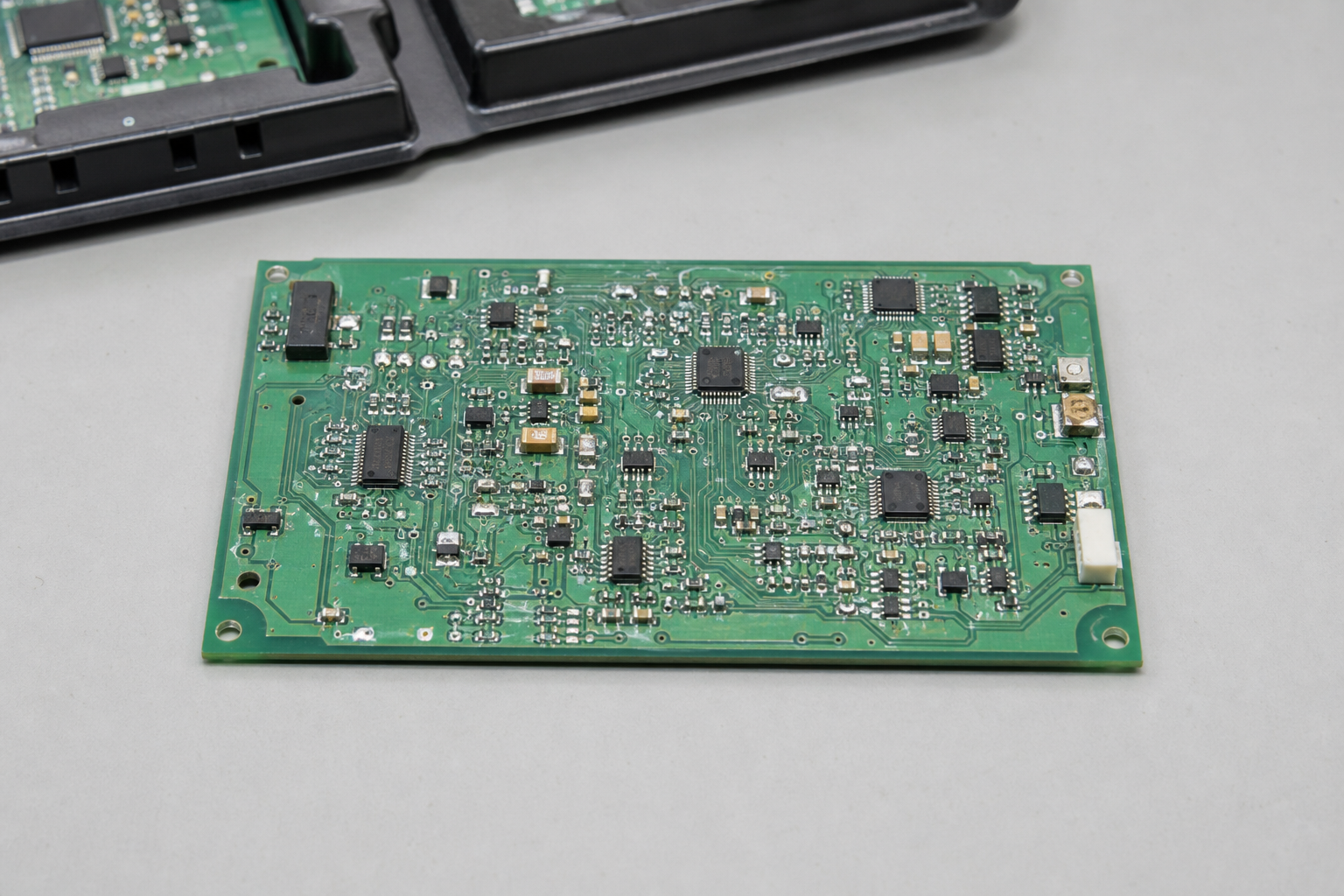
Commodity Output
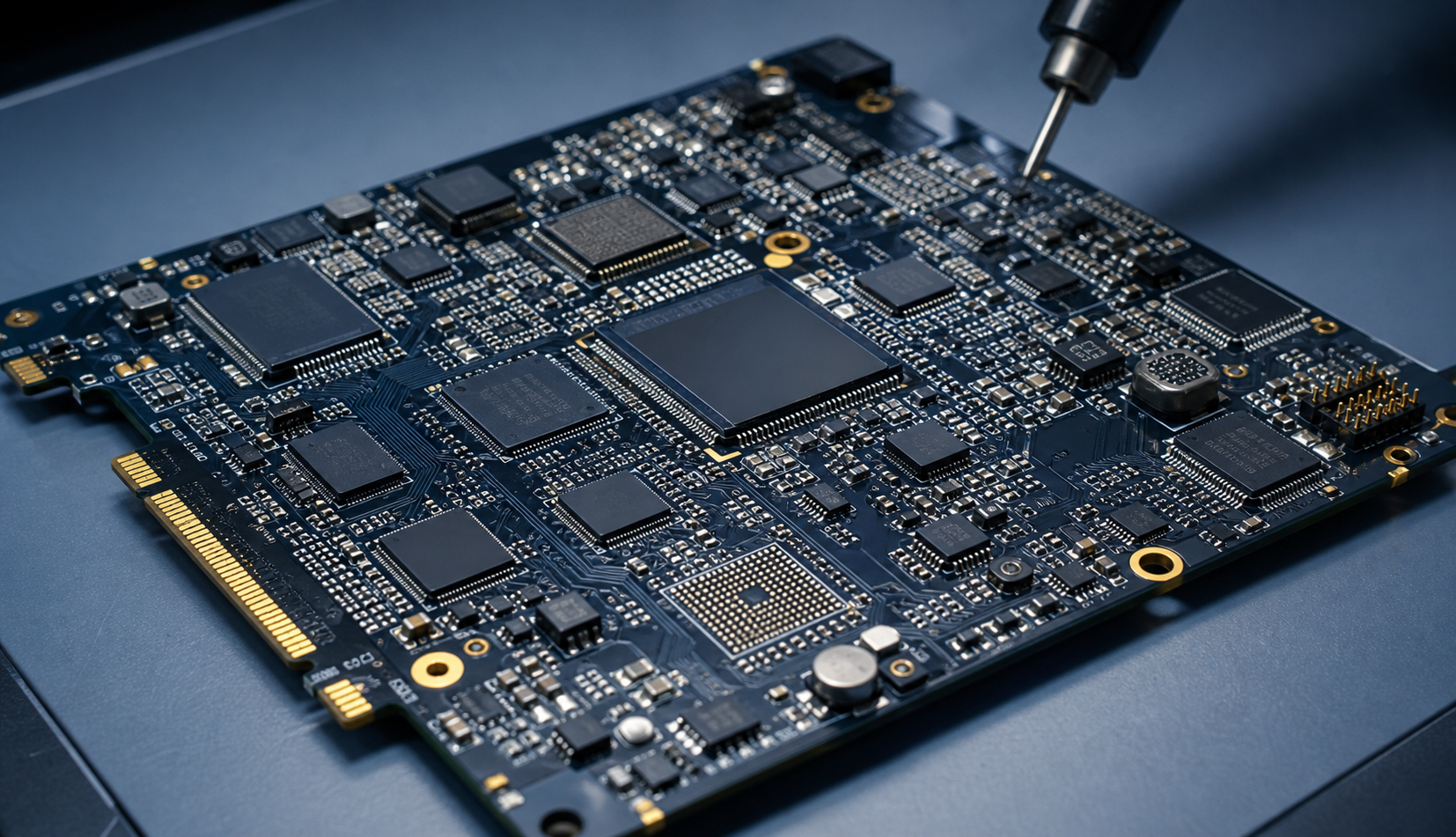
PCBark Engineered
The Real Cost of Offshore PCB Assembly: A Landed-Cost Ledger
The number that can change an offshore project is the delivered cost, not the line-item assembly price. For China-sourced PCBA, import treatment depends on board function, component origin, shipment value and current tariff rules. PCBark itemizes FOB price, freight, duty assumptions and customs-related fees in the quote so your purchasing team can review landed cost before ordering.

PCBA Landed-Cost Ledger
| FOB factory price | $25,000 |
| Ocean / air freight | ≈ $1,500 |
| Duty / tariff assumption | Quote-specific |
| Customs + broker fees | ≈ $400 |
| Estimated landed cost | Calculated before order |
Before PO
PCBark separates product cost, freight, tariff assumptions, broker fees and optional test scope so buyers compare delivered cost instead of headline unit price.
Two landed-cost details to check before ordering.
First, classification: a bare PCB and a populated PCBA may be treated under different headings depending on function and destination. PCBark flags the likely classification assumptions for broker review instead of treating HTS as an afterthought.
Second, quote assumptions: consigned components, country-of-origin rules, tariff exclusions and duty programs can affect the dutiable base. Because these rules change, PCBark treats tariff line items as quote assumptions for your broker to validate, not as legal advice.
Certifications, Standards and Capability Boundaries
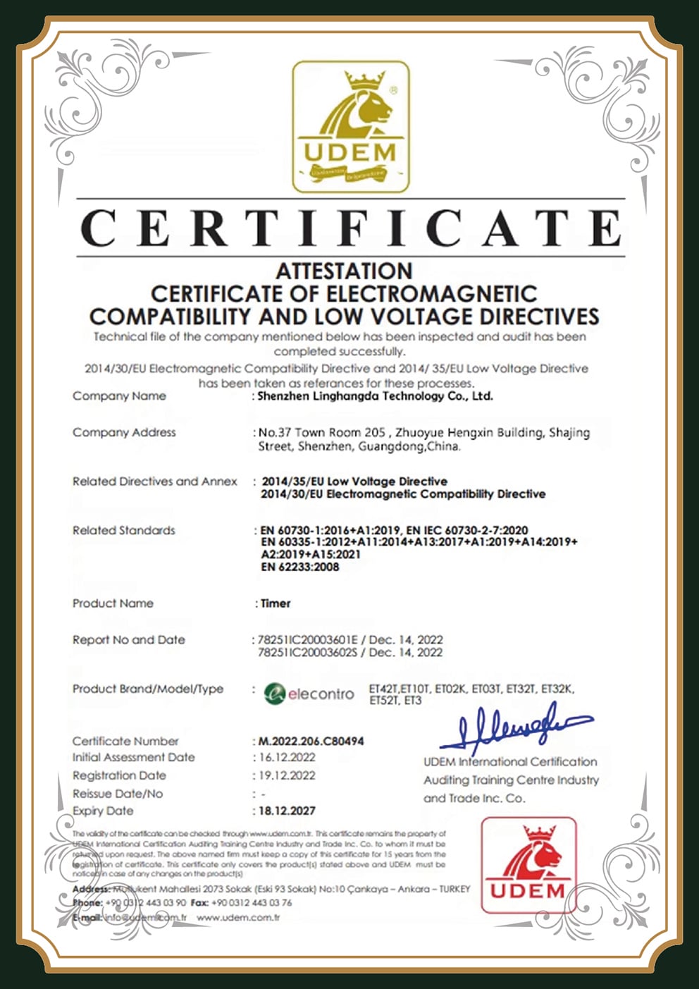
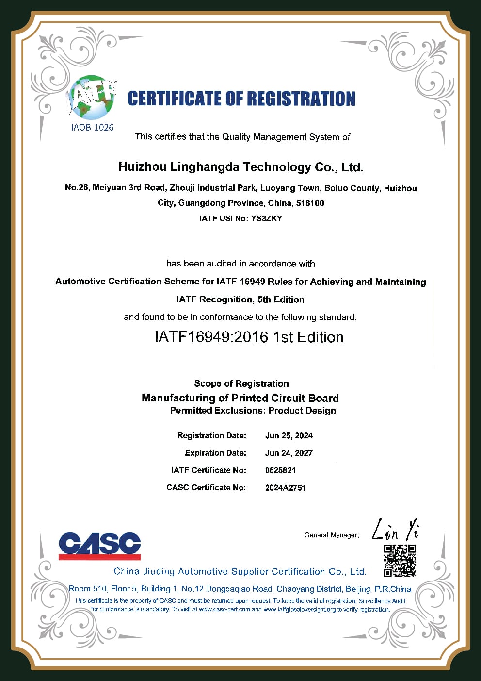
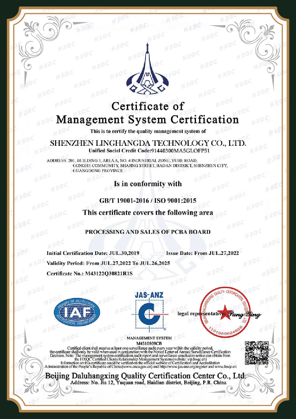
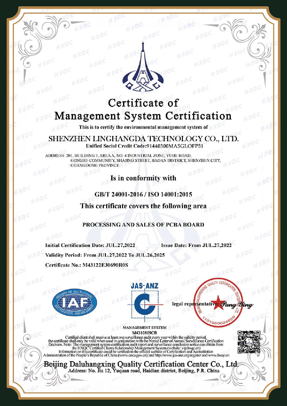
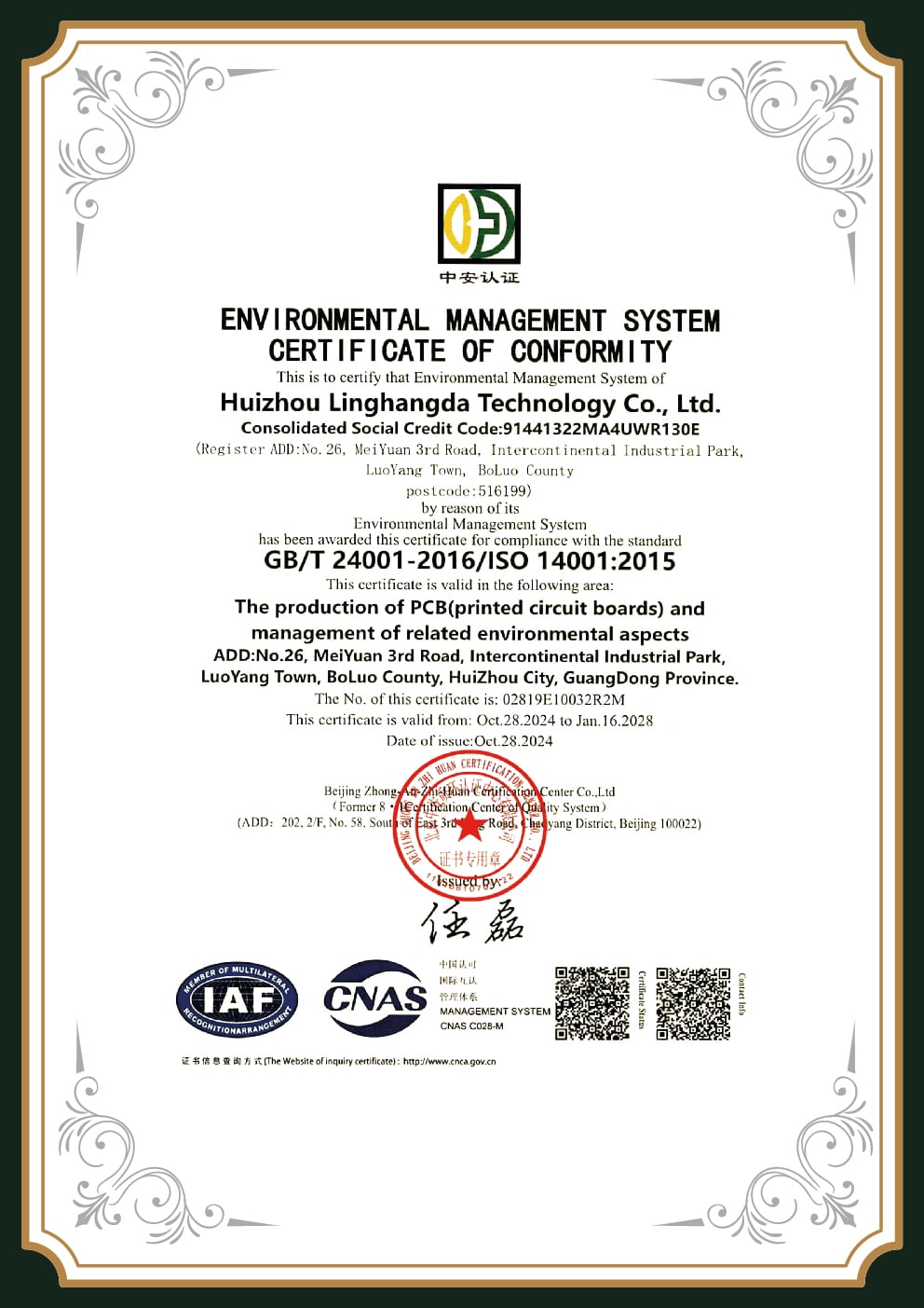
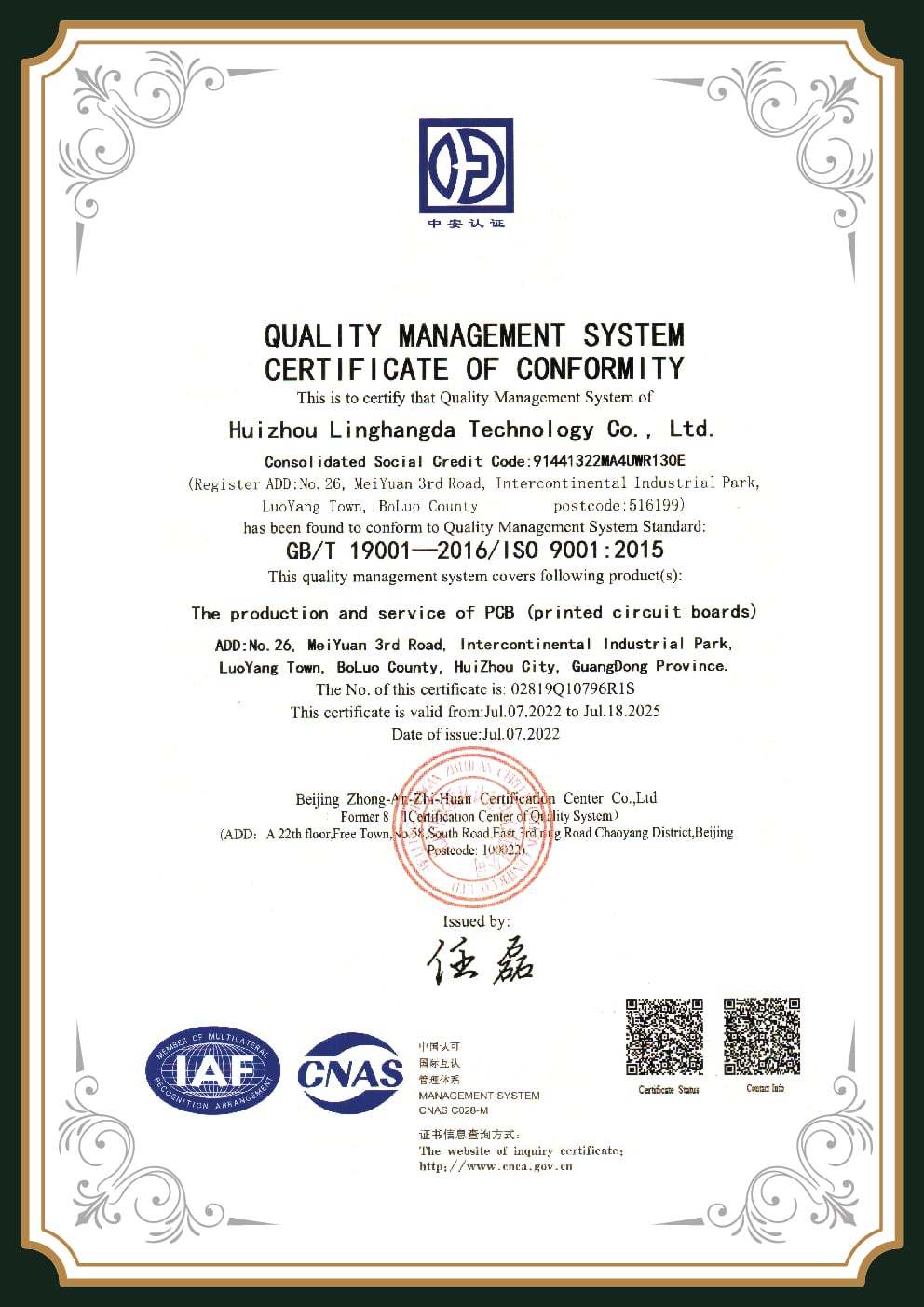
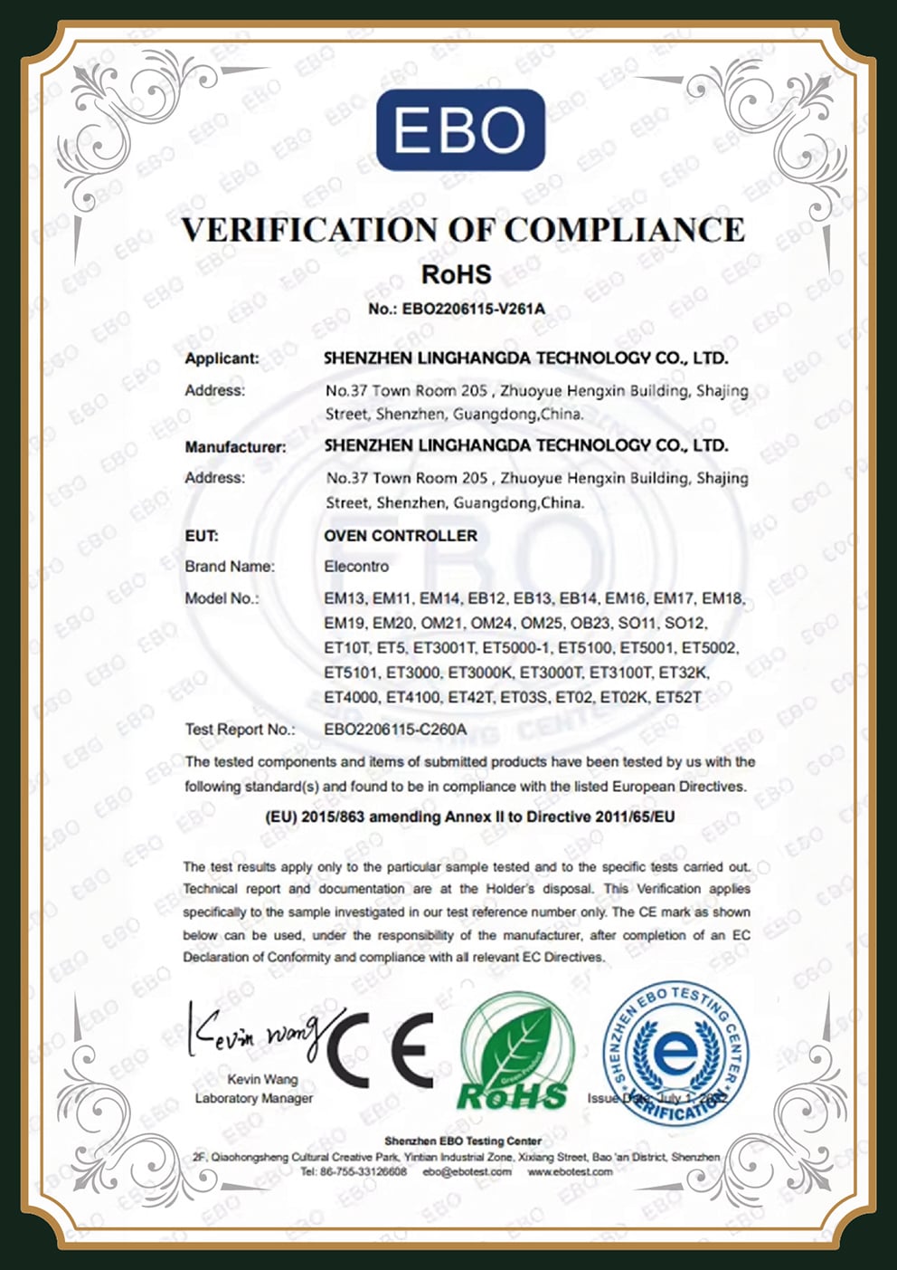
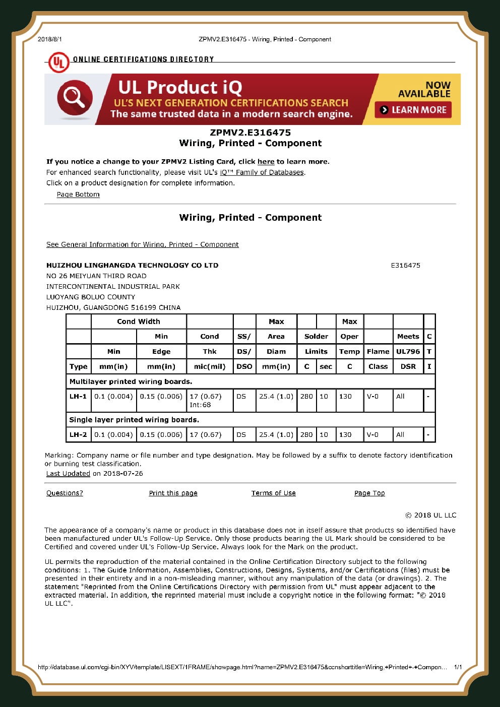
Certifications are a system, not a logo. PCBark assembles to the standards below and keeps the lot, date and inspection records that let you verify it, because a stated standard you can’t audit is worth nothing.
8 Certs Auto-playing
ISO 9001:2015
Quality management
ISO 14001
Environmental
IPC-A-610 Class 2/3
Assembly Acceptability
J-STD-001
Soldering process
UL
Recognized
RoHS / REACH
Materials compliance
Core Assembly Standards
The two standards that matter most on the floor are complementary: IPC-A-610, run under our ISO 9001 system, defines whether the finished assembly is acceptable, and J-STD-001 defines the soldering process used to build it.
Both share the same Class 1/2/3 framework, and the jump from Class 2 to Class 3 is concrete, not marketing.
Notice: A common misconception ties Class 3 to aerospace alone. It does not. IPC class is chosen by the reliability requirement of the end product, not by industry label, so Class 3 can also apply to critical industrial controls, automotive safety electronics and medical electronics. Pick the lowest class that genuinely meets your reliability needs; over-specifying Class 3 adds cost without value.
| Acceptance criterion | Class 2 (Dedicated) | Class 3 (High Rel) |
|---|---|---|
| Plated-through-hole fill | 50% minimum | 75% minimum |
| Copper voids in barrel | 1 void in ≤5% of holes | None |
| Min plating thickness | 0.8 mil | 1.0 mil |
| Annular ring | ≤90° breakout allowed | No breakout — unbroken |
| Solder wetting (solder side) | 270° | 330° |
| Inspection regime | Sampling, AOI common | 100% + X-ray |
Capability Boundary for Regulated Programs
PCBark does not hold AS9100D, ITAR registration or ISO 13485. We do not accept ITAR-controlled defense work, AS9100 aerospace programs or Class III / implantable medical-device programs that require those systems. For commercial, industrial, consumer, IoT and non-safety-critical automotive PCB assemblies, PCBark supports IPC-A-610 Class 2 or Class 3 workmanship, ISO-system documentation, inspection records and practical engineering review.
Click anywhere to close
PCBA Engineering & Cost Intelligence
PCBA Landed-Cost Estimator
See your real China→U.S. delivered cost — FOB + freight + Section 301 duty + fees — before you order.
Initialize Tool
Assembly-Type Routing Selector
Answer three questions and we’ll route your board to the right PCB assembly service.
Select Route
IPC-A-610 Class 2 vs Class 3 Selector
Pick the lowest class that meets your reliability need — over-specifying Class 3 adds cost without value.
Analyze Standards
A PCB assembly, or PCBA, is a bare printed circuit board that has been populated with its electronic components, resistors, capacitors, integrated circuits and connectors, and soldered into a finished, working unit through surface-mount and through-hole processes. The bare board only carries the copper pathways; the assembly step adds every active and passive part, then proves the result with inspection and electrical test before the PCB assemblies ship to you.
A PCB is the bare, unpopulated board, copper traces on an insulating laminate with no components, while a PCBA is that same board after parts have been mounted and soldered, which is the version that carries component cost, assembly labour and a different customs classification entirely.
Fabrication builds the bare board itself, etching the copper, laminating the layers, drilling and plating, while assembly is the later step that places and solders components onto that finished board, which is why a full turnkey order at PCBark moves straight from our PCB manufacturing line into assembly under one roof and one PO.
Assembly cost is driven by component count, placement time, package difficulty, volume, turnkey model and test coverage. The figure that sets your budget is delivered cost: FOB price, freight, tariff assumptions, customs fees, inspection scope and any rework or expedite charges. PCBark itemizes these pieces so purchasing can compare quotes on the same basis.
For prototype and low-volume runs, expedited builds may be available for small quantities once PCB files, BOM, components and engineering questions are complete. Standard lead time depends on component availability, quantity, inspection scope and the selected build window.
Ask for an itemized quote first, because a single total price with no breakdown is the clearest sign that testing, sourcing control or engineering review is quietly missing from the number you’re comparing. Then confirm the inspection and test steps, the workmanship class (IPC-A-610 Class 2 or 3), the traceability and certificate-of-conformance records that prove it, and who answers your engineering questions, a house that documents its standard beats one that’s a few cents cheaper per board.
No, and we say so plainly: ITAR-controlled defense work, AS9100 aerospace programs, and ISO 13485 Class-III or implantable medical devices all require a U.S. facility or registrations that PCBark does not hold, and U.S. export law bars a China factory from handling ITAR-controlled technical data at all. We build commercial, industrial, consumer, IoT and non-safety-critical automotive PCB assemblies to IPC-A-610 Class 2 and Class 3, and when your project falls outside that scope we tell you up front and point you to a shop that can take it.