Get in touch with PCBark Company


Prototype PCB assembly is the process of populating a manufactured blank board with components and testing it, turning a Gerber file and a BOM into a tangible, operating circuit with which you can interact. It lies between manufacturing the board itself and going into mass production, and is the very first place that the actual behavior of your circuit (as opposed to the circuit’s schematic logic) can be tested.
Quick Specs
| Typical first-run quantity | 3-10 boards (single-board runs risk a false pass) |
| Hand-solder practical limit | Down to roughly 0201 passives / 0.4-0.5mm pitch, per industry guidance |
| Minimum file package | Gerber (RS-274X/IPC-2581) + BOM with MPNs + CPL/centroid file |
| Cost structure at 1-5 boards | Dominated by fixed setup (stencil, programming, first article), not components |
| Governing standards | IPC J-STD-001 (soldering), IPC-A-610J-2024 (acceptance), IPC-2221 (design) |
In short: Prototype PCB assembly turns a design file into a testable board. Most first-time builders lose time not to the assembly process itself, but to decisions made before the order ever goes out — whether to hand-solder, what files to send, and how many boards to build. This guide walks through those decisions in order, using a hand-solder threshold, a cost-structure breakdown, a first-run failure catalog, and a design-maturity framework you can apply regardless of which assembler you use.
TL;DR
- Parts finer than approximately 0.4 to 0.5mm are well above anything reliable hand soldering can provide, and is quite literally above that line (and then some).
- Perhaps the most likely cause of a first quote being stuck or incorrectly generated, the absence or positioning error in the centroid file.
- At 1-5 boards, it’s the fixed setup charge, not the parts, that dominates your per-board cost.
- There are typically a half-dozen repeatable culprits behind nearly all first-prototype failures; they’re not just bad luck.
- Three gate readiness checks (stolen from engineering approaches to managing risk) can give you insight into whether you’re truly ready to exceed prototyping volumes.
What Is Prototype PCB Assembly (and When You Actually Need It)
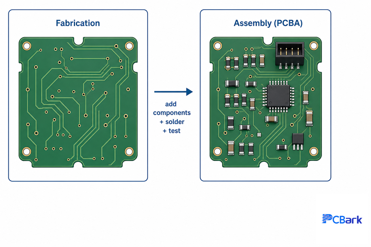
A prototype PCB assembly isn’t a prototype PCB fabrication. Fabrication makes the bare printed circuit board (the board itself, including traces, solder mask, silkscreen, plated holes, etc) without anything mounted to it. An assembly, often called a PCBA or printed circuit board assembly, involves putting the physical components (resistors, ICs, connectors, etc) onto the board and soldering them into place, and then testing the board.
If you only need to see if a board fits a housing or check the impedance target of a stack-up, the fabricated bare board may be all you need. If you intend to plug in power, load some firmware, and see if the sensor reading makes sense, you need to order an assembled prototype.
And the difference makes a difference to what gets shipped and who gets shipped to – a reminder that you’ll encounter from time to time any time “printed circuit board” appears as a generic catch-all that might be describing just the bare board or a complete assembly. Fabrication-only customers send in the Gerber and drill files. Customers for complete assemblies need to supply a bill of materials, a placement file and, for many modern designs, parts with component packages small enough to fit the fabrication equipment at the PCB house.
Getting this distinction wrong costs real time: a surprising number of first-time buyers request “quick turn prototype pcb” fabrication only, then discover mid-project that they actually needed a fully populated board to test firmware – triggering a second order and a second lead-time cycle. The NASA training curriculum built on IPC J-STD-001 treats fabrication and assembly as two distinct process domains with separate acceptance criteria for exactly this reason: a board can pass every fabrication inspection and still not be an assembly-ready product. Any PCB assembly service worth using will ask which one you actually need before quoting, rather than assuming. Most printed circuit board assembly services split cleanly along this same line: a pure-fabrication pcb service quotes bare boards only, while full pcb assembly capabilities cover file review, sourcing, and populate-and-test in one order.
What Is PCB Prototype Manufacturing?
PCB prototype manufacturing covers both fabrication (making the bare board) and assembly (populating and testing the finished boards) for a small (1-25) pre-production batch of prototype boards constructed to verify the design before committing to manufacturing. Normally the same processes used for production are used (e.g. solder paste printing, pick-and-place, reflow soldering) but on flexible, short-turn-around lines rather than on long production runs. The aim isn’t maximum efficiency, but knowledge: how does it behave, and is it ready to go?
Exporting clean files from your pcb design software during the design phase – not scrambling to fix them after a vendor flags an issue – is what keeps a pcb assembly prototype run on schedule.
Hand-Assembly vs. Professional Prototype Assembly: The Hand-Solder Ceiling
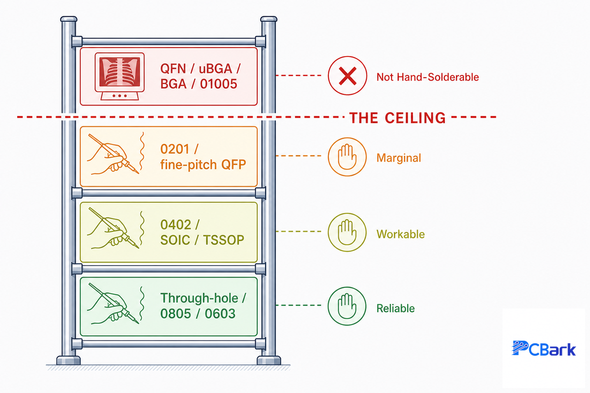
The Hand-Solder Ceiling is where a design’s component packages stop being hand-solderable for practical purposes no matter who holds the iron. Below the ceiling, hand-assembly is an entirely valid, and in fact quite popular, approach – most boards made by hobbyists, and in the very early days, much of professional boards, were done by hand. Above the ceiling, the physics of the solder joint get very much in the way of manual methods, and the defect rate goes up, not down.
| Package Type | Hand-Solder Feasibility | Why |
|---|---|---|
| Through-hole, 0805/0603 passives | Reliable | Pads and pitch are large enough for visual alignment and manual iron control |
| 0402 passives, standard SOIC/TSSOP | Workable with practice | Small but still individually addressable with fine-tip tools and magnification |
| 0201 passives, fine-pitch QFP | Marginal — expect defects | Approaching the ceiling; tombstoning risk rises sharply as thermal mass drops |
| QFN, uBGA, BGA, 01005 | Not hand-solderable | Joints are hidden under the package body — there is no way to inspect or rework by eye or iron |
There’s a reason this is a cliff and not a slope. Thermal balance. A 0201 passive weighs about a milligram and has virtually no thermal mass; a mere 2-3°C difference between its two pads during a reflow cycle will pull it upright before solder wetted both sides.
The NASA training standard (based on IPC J-STD-001) dedicates separate modules to through-hole and surface-mount soldering for exactly this reason – the physics that work for one family of packages breaks down as the pitch gets smaller. With QFN and BGA devices, where terminations are on the underside, there’s no way to even visually inspect a joint, much less make corrections. X-ray inspection is the only way to check those joints from that point on.
⚠️ Important
It’s tempting to think that hand-assembly will be cheaper/slower; once you figure in the real cost of doing it wrong, that advantage vanishes. Setting up a professional run has heavy front-loaded fixed costs (see below); you can wipe out the “savings” from hand-soldering a marginal board with one single defect requiring a rework and a second board spin.
Getting Your Design Assembly-Ready: Files, Formats, and What Trips Up First-Timers
So What Exactly Does PCB Prototyping Involve?
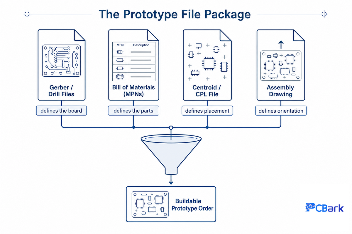
PCB prototypes ship with three related files that have to match perfectly: Gerber/drill files to define the board layout, a bill of materials (BOM) listing every part by manufacturer and part number, and a centroid (CPL/pick-and-place) file for guiding the assembly machines. New designers typically get the Gerbers (they’re usually auto-generated from your CAD) and mess up the other two files.
- BOM lists the manufacturer’s part number for each line item, not just generic part types like “10k resistor”.
- Centroid file orientation and origin match your board layout, not your CAD software’s default coordinates.
- BOM reference designators match the board’s silkscreen print and the centroid file exactly.
- Polarities and pin 1 designations are clearly indicated so the assembler doesn’t have to guess.
- Every file in the shipment (Gerber, BOM, centroid, assembly drawing) is for the same revision of your design.
Missing or improperly scaled centroid files are among the most frequent causes of the initial prototype quote being delayed or of parts being placed in the wrong location on a completed board – a placement offset of even 0.1mm on a 0.4mm-pitch part is enough to cause an open joint. This is also one of the simplest problems to avoid; unlike a design error, it doesn’t involve engineering a new solution-it simply requires verifying that the file exists, and that its units and origin match the board, before you click “Submit”.
📐 Engineering Note
If your board ties any pad – through-hole or thermal – into a solid copper plane on 1oz or heavier copper, that plane is a heat sink during soldering. This is normal PCB design practice which is referenced throughout the entire IPC-2221 family of printed-board design standards; the same rules are incorporated here as a thermal relief spoke pattern – a narrow copper bridge connecting the pad to the plane, instead of a solid tie – which prevents that connection from starving the joint of heat during reflow or hand-soldering. Consult your fab house on which specific edition and section they design to, since standards are periodically updated. Failing to include this on a heavy ground plane is a common cause of cold joints that will seem perfect on visual inspection but still fail once-in-a-while in the field.
While PCBark’s own DFM readiness checker and similar tools from the majority of assemblers will automatically catch the structural design-rule violations – annular ring, trace spacing, solder mask clearance – this section focuses on the file-package layer those tools can’t verify: whether what you send is complete, consistent, and describes the board you actually want built.
Design and assembly are two separate disciplines with their own failure modes: a board can pass every board manufacturing inspection and still be unassemblable, just as a board can be perfectly populated and still fail because of a stack-up problem baked in at layout. Impedance control matters here too – on multilayer boards a mismatched trace width or missing reference plane will corrupt a signal long before assembly ever touches it, and it’s far cheaper to catch during the design phase than after boards are populated. Late design changes discovered post-order are one of the more expensive ways to relearn that lesson.
SMT, Through-Hole, or Mixed: Matching Assembly Technology to Your Prototype
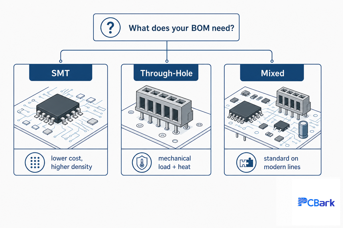
Most modern designs default to surface-mount technology (SMT) because it supports higher component density and lower placement cost per joint. However, through-hole (THT) hasn’t disappeared from prototype boards and the reason is purely mechanical: a 2021 Microelectronics Reliability study testing solder joints across 550 thermal cycles spanning -20°C to +80°C specifically identified THT as the essential choice when a joint has to bear real mechanical load or remove significant heat – connectors, large electrolytic capacitors, and power devices subject to repeated insertion force or thermal cycling in the field.
| Your BOM Looks Like | Choose | Why |
|---|---|---|
| Mostly ICs, passives, no board-edge connectors carrying real force | SMT | Lower per-joint cost, higher density, faster placement |
| Board-edge connectors, power components, anything user-facing that gets plugged/unplugged | Through-hole for those parts | Mechanical retention and thermal dissipation the surface-mount pad alone can’t provide |
| Both of the above on one board | Mixed technology | Standard on modern lines; a mixed assembly costs a modest premium for the extra process step, not a fundamentally different build |
For a first prototype in particular, resist the temptation to force every part into SMT footprints just to save on build time. Connectors undergoing real insertion cycles during bench testing are precisely the sorts of joints you don’t want to fail mechanically while you’re working out the firmware.
On the shop floor, matching technology to your BOM plays out as a straightforward process flow: solder paste printing, a pick and place machine setting every part, reflow at a profile commonly peaking near 245°C for lead-free alloys, then inspection. Modern pick-and-place machines handle both SMT and through-hole insertion points on the same line, which is a large part of why mixed-technology boards no longer carry the cost penalty they once did. Automated optical inspection catches most visible placement and solder defects immediately after reflow, 3D X-ray catches the solder-joint defects hidden under a component body that AOI can’t see, and functional testing – actually powering the board, probing it with an oscilloscope, and checking it against your pass/fail criteria – is what confirms the design works, not just that it was built correctly.
What Actually Drives Prototype PCB Assembly Cost, The NRE-to-Piece-Price Split
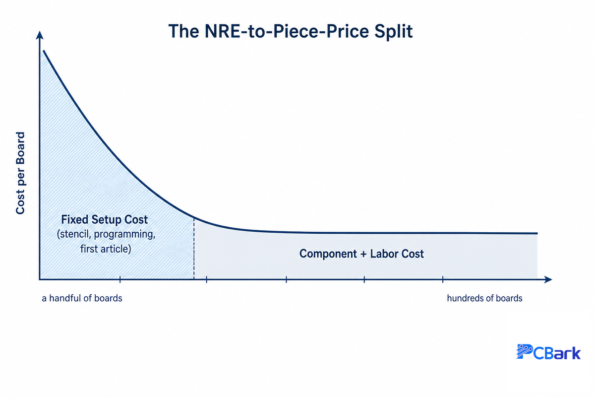
Prototype assembly quotes often appear costly per board in comparison to production pricing, and the reason is rarely that the components or labor costs are higher at low volume – rather that non-recurring engineering (NRE) costs are flat per job, not per board. The NRE-to-Piece-Price Split defines this: that your per-board cost at prototype quantities is dominated by costs that don’t scale downward with quantity: stencil fabrication, pick-and-place programming, first-article inspection setup.
Industry pricing patterns typically illustrate this directly: a setup cost in the $200-$400 range (stencil, programming, first-article inspection combined) adds roughly $40-$80 to each board on a 5-board initial run, but only a few cents per board once that same fixed cost is amortized across a 1,000-unit run 6-12 months later – with no change to the processes behind it. This is why the same design can appear drastically cheaper per piece once you’ve scaled from five boards to five hundred, despite there being no change to how it’s manufactured.
Where Your Prototype Dollar Actually Goes
- Fixed setup – stencil, placement program, first article inspection. A stencil alone commonly runs $30 to $150, on top of programming and first-article costs. Paid for once per job regardless of quantity.
- Components (BOM) – the cost of your components scales directly with quantity, because at low volumes you generally won’t get direct from supplier pricing and you’re paying for a piece price through distribution.
- Assembly labor / machine time – This is largely driven by placement count, and the complexity of your board layout; roughly linear with quantity.
- Test and inspection – this scales per board, although the fixture or program cost supporting it’s fixed, like setup.
Why this split matters when making decisions on your first order is that it tells you what you should actually negotiate over. Reducing the cost of a specific component will make a negligible difference for 5 boards because it’s not where your money is. However, grouping another design revision on your second order with this first, or changing your turnaround from a rush to standard will have a much bigger impact because they both reduce the frequency at which you have to pay for the setup fees.
This is also the trap in chasing the “cheapest pcb manufacturer” quote for a prototype run: a vendor advertising the lowest per-board price often gets there by minimizing exactly the fixed-cost items – a thin DFM review, no first-article inspection – that catch problems before they reach production. A patented failure-analysis methodology for electronic components makes the same point from the engineering side: predicting where a design is likely to fail before it’s built is cheaper than discovering it after, which is exactly what a stripped-down setup process skips. When comparing prototype pcb assembly price across suppliers, ask what’s actually included in that per-board number, not just what the number is.
Why First Prototypes Fail: The First-Article Fault Tree
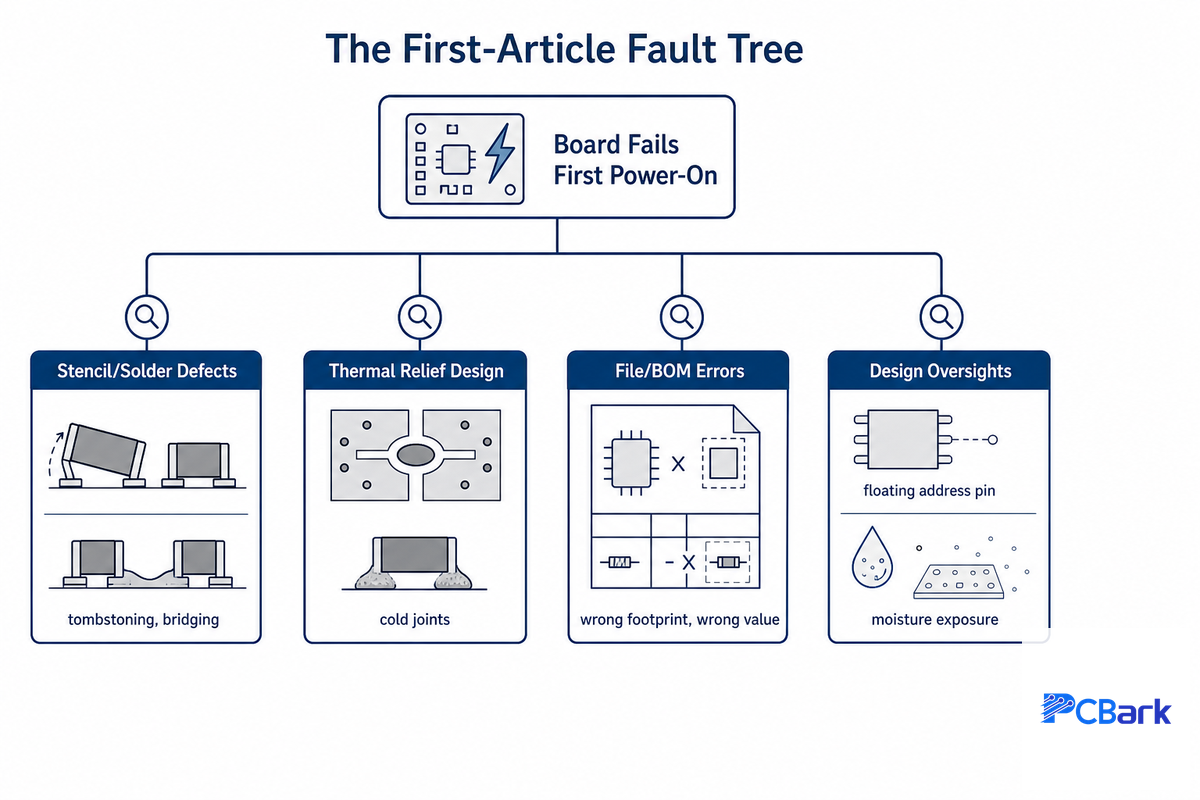
As you’ll find reported throughout the technical literature on manufacturing and assembly, over 70% of assembly stage defects are linked back to the first manufacturing step a board goes through: the stencil printing. This first process occurs before a single component is placed, and it reveals a key insight: most first prototype failures aren’t random events. Academic work on solder joint thermal-cycling reliability traces the same pattern down to a mechanism: repeated fatigue driven by CTE mismatch, not random chance.
In fact, by looking at a First-Article Fault Tree, you can identify a small set of recurring, repeatable root causes for the failures, instead of having to analyze every one as a completely new problem.
“There’s rarely anything ‘magical’ about the reasons why a first run board fails the first time it’s powered up. They nearly always fail for a reason you should have already found if you’d looked for it properly. When we review boards coming back from the factory floor that are DOA, the same handful of causes keep showing up over and over again in different disguises.”
| Failure Type | Likely Root Cause | Prevention |
|---|---|---|
| Tombstoning (small passive standing on end) | Thermal imbalance between the two pads as the board moves through the reflow oven, often triggered by a ramp faster than roughly 1-2°C/second, not a placement error | Keep both pads within 10% of the same copper area and thermal mass; avoid tying one pad into a large copper pour without a thermal relief |
| Insufficient solder / open joints on fine-pitch parts | Stencil aperture area ratio below roughly 0.66, too thick or too narrow for the paste to release cleanly | Confirm stencil area-ratio is adequate for apertures under 0.5mm before ordering; a 100-120µm foil often outperforms a thicker one on fine-pitch parts |
| Solder bridge between adjacent pins | Excess paste volume or stencil misalignment on pitches under 0.5mm | Verify stencil-to-pad alignment tolerance and paste volume before the full panel runs, not after |
| Cold joint that reads fine but fails intermittently | Through-hole pin tied directly to a heavy (1oz+) copper plane with no thermal relief | Use thermal relief spoke connections per IPC-2221 Section 9.1.4 instead of a solid plane tie |
| Board builds clean but simply doesn’t work electrically | Footprint/pinout mismatch that electrical rule checks can’t catch, because they only know what you drew, not the real part | Cross-check every footprint against the current manufacturer datasheet, not a shared library part |
| Wrong value part installed and passed visually | BOM line described generically (“10k resistor”) instead of by manufacturer part number, letting a substitution slip through | Lock every BOM line to a specific MPN with approved alternates, never a generic value description |
| Component reversed or misoriented | Ambiguous or missing pin-1/polarity marking in the centroid file or silkscreen | Mark polarity and pin-1 orientation explicitly on the assembly drawing, not just the silkscreen |
| Intermittent failures appearing only after handling or storage | Moisture-sensitive components exposed beyond their floor life before reflow | Follow moisture-sensitivity handling guidance (the J-STD-020/033 standard family) for any MSL-rated part, especially after a board sits between design revisions |
| Address conflict between two identical sensors/ICs | An address-select or enable pin left floating instead of tied to a defined logic level | Verify every configuration pin has a defined state in the schematic, not just in the datasheet’s typical application circuit |
As two accounts from forum participants working through their very first PCBs show, these root causes often aren’t the high-tech surprises we’d imagine, but the most basic oversights. One reported tracing a non-working board to two sensors sharing the same address because an address-select pin was left floating rather than tied to a supply rail — a design decision, not a soldering defect. Another reported finding “about a dozen issues” on a first prototype, mostly incorrect footprints and wrong-value resistors.
Fixing these problems at the beginning can save a lot of money, beyond just your peace of mind. One report on the costs of defects in the electronics industry found that fixing a defect caught before reflow soldering costs roughly $0.44, versus roughly $550 once it reaches the field after shipment – over 1000 times as much. The value proposition for checking a design against a known fault list before it leaves your hands for the first time makes itself immediately clear through the sheer economics of the matter.
From Prototype to Production: The 3-Gate Design-Maturity Framework
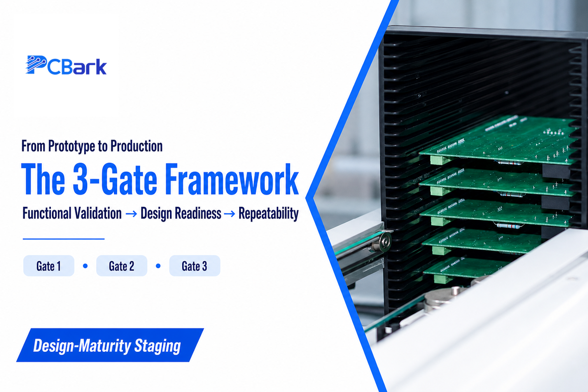
The 3-Gate Design-Maturity Framework directly answers the question that nearly all first-time PCB designers eventually ask themselves at some point in the prototype process: “How many rounds of prototyping will it take before my board is ready for mass production?” This framework mirrors the approach documented by the U.S. Government Accountability Office for large acquisitions programs and their well-established knowledge-based gates used to mitigate risk when investing large sums of money in unproven systems – the application of the concept to your prototype PCB project is intended to offer practical guidance, not a dogmatic approach.
The Three Gates
- Gate 1 — Functional Validation: Is the fundamental design sound against its original requirements? Some teams simulate expected electrical or thermal behavior before tooling up, but simulation doesn’t replace a populated board coming back from reflow and getting tested against the real world. Don’t over-build your boards; leave test points, debug headers, and programming access in place for this stage as you’ll want to find and fix issues.
- Gate 2 — Design Readiness: Is the design stable, so subsequent work is refinement rather than redesign? At this point, a completed DFM with no open issues, a locked Bill of Materials with approved alternatives, and a stackup matching the final mechanical outline should be complete.
- Gate 3 — Repeatability: Have at least two iterations proven the production process (not just the design) capable of reliably building a working board? This is something a single working prototype can’t demonstrate.
Too often, companies treat every build of a prototype as being the same – no matter which stage it’s supposed to prove.
A prototype used to find and fix design flaws needs to be as open as possible (messy files and mid-build modifications are the norm at Gate 1), whereas a prototype used to verify production-readiness needs to be stable enough that no further design tweaks are being introduced – and if they’re, that’s an indicator the prototype missed a gate.
How to Order Your First Prototype PCB Assembly (A Vendor-Agnostic Checklist)
How Can I Place a PCBA Order?
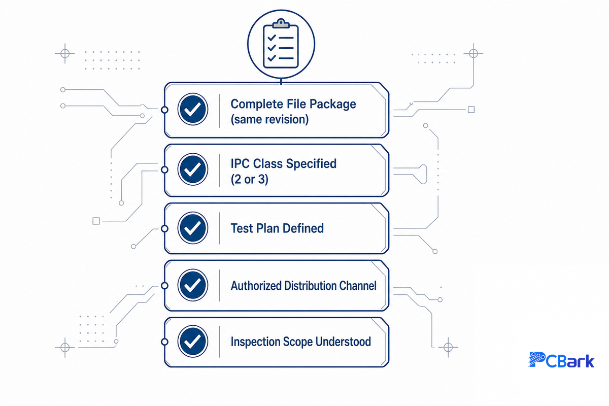
Whether you’re ordering from a large overseas firm or a local quick-turn facility, ordering prototype PCB assemblies hinges on a ready file package, a clear IPC class expectation, and asking the right questions before you commit to a vendor.
This checklist applies equally, regardless of order size or turnaround time:
- A complete file package including Gerber/drill files, Bill of Materials (with part numbers), centroid data, and an assembly drawing – all on the same revision
- An IPC class (Class 2 for most consumer and commercial products; Class 3 for those that must perform in demanding environments for extended periods).
- A test plan, at least to the extent of a power-on sequence, required voltage rails and a pass/fail criterion. You should have an understanding of what “working” looks like before boards show up.
- Assurance that any single-sourced component is procured through an authorized distribution channel, not the open market.
- Understanding of which inspection services (optical inspection, and possibly X-ray of BGA and QFNs) are included and which are optional and how they affect turn time and cost.
Beyond the basic list, three specific questions help distinguish between a vendor who will find and address issues before your prototype arrives versus one that simply produces what you send: Is the design reviewed by a human engineer or just automated design rule checking?
What do they do when a Bill of Materials entry is ambiguous?
And is first article inspection included, or a paid add-on?
If you prefer not to do this vetting yourself, PCBark’s prototype PCB assembly service uses our production-certified lines with a complimentary DFM review for every job.
Choosing the right manufacturing partner matters more for a small run than it does once you’re placing large recurring orders, because a partner who delivers consistent quality on a 5-board prototype run is the one you actually want handling your 5,000-board production order later. If your design also needs a full box build assembly beyond the bare PCBA, confirm that scope is covered by the same vendor before you split the order across two suppliers – and be skeptical of any quote promising low costs without explaining what’s excluded from it. Understanding the full pcb assembly process end-to-end, not just the assembly step in isolation, is what lets you ask the right questions at each stage.
Industry Outlook: What’s Changing in Prototype PCB Assembly for 2026
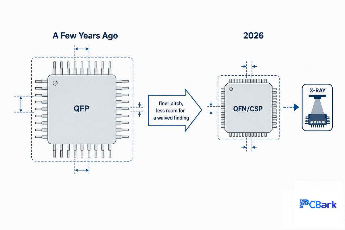
What’s changing prototype PCB assembly going into 2026 is clearly not price-it’s risk. Denser components and finer pitch packaging are going from rare to standard on most new designs and with each step lower in pitch, we chip away at the margin for error at the exact time a design first faces scrutiny – first article assembly. Whereas two years ago, a PCB design would likely employ an 0.8mm-pitch QFP package, that board likely has a 0.4mm-pitch QFN or CSP today pushing designs over the Hand-Solder Ceiling, thus increasing the importance of the file-preparation and DFM-review phases of your design as previously outlined in this guide. Automated inspection is picking up part of that slack – automatic optical inspection systems designed for exactly this kind of dense, fine-pitch board are becoming standard rather than optional on assembly lines built for 2026-era designs.
What that practically entails: allow more review time at the back end, not less, in spite of design tool advancements that accelerate layout-the DFM check that required a 24-48 hour turn for a 0.5mm pitch board two years back can take 3-5 days now on a 2026 layout that features both 01005 passives and a 0.4mm pitch BGA. As of right now, if you’re lining up a 2026 production run with any mixed technology and fine pitch elements, consider the DFM check to be something of an absolute, a required check point, as opposed to a discretionary pass. A waived finding against a 0.4mm-pitch part is far more likely to become a field failure than the same waived finding was on yesterday’s coarser-pitch designs.
Market size projections for the overall PCB assembly sector ($100 billion for 2025-2026, per a few estimates) are useful context, and nothing more.
Frequently Asked Questions About Prototype PCB Assembly
Q: How many prototype boards should I order for a first build?
View Answer
Usually a first pass at a prototype is somewhere between 3 and 10 boards per engineering team – never one board. With a single board, you learn if that board actually works; you cannot learn if that board can be repeated (a suspect solder joint or a tolerance near the limit of the range can pass on one board, fail on another). Placing an order for several units at once will catch many of the same first-time file-package issues (check out the checklist above) within a single order rather than resulting in two submissions and two waiting periods.
Q: Can I hand-solder my own PCB prototype instead of using an assembler?
View Answer
Yes, if your design stays below the Hand-Solder Ceiling of 0402-and-larger passives and standard-pitch ICs (no blind termination packages). The second the BOM includes QFN, BGA, or 01005 parts, hand-soldering shifts from a question of reliability to a matter of physical reality-those solder joints are hidden by the component, and cannot be inspected or re-worked except using reflow-grade tools and an X-ray machine.
Q: What’s the difference between a bare PCB prototype and a prototype PCB assembly?
View Answer
A bare PCB prototype is simply the board that was manufactured with all of the layers, the solder mask, and drilled holes, but without any of the electronic components attached. When you attach all the parts to that bare PCB and then probably test it, it is now called a prototype PCB assembly. A bare board may be used to check fit within a mechanical design or to test a manufacturing process, whereas an assembled board is necessary to check for proper electrical operation.
Q: What causes a first prototype run to fail testing?
View Answer
Most first-run failures have less to do with random bad luck than a few repeatable failure modes, which are fully broken out in the First-Article Fault Tree shown above. These are, roughly: small components tombstoning from a thermal imbalance during reflow; solder joint starving or bridging from stencil printing defects; large-plane thermal-relief design flaws on a component; footprints or pinouts that electrical-rule-check okay but don’t match the physical part; and moisture-sensitive components exposed for too long before assembly. Nearly every one of these failures can be eliminated during the design review, before a board is ever produced-and at a tiny fraction of the cost of addressing them after they ship.
Q: What’s a Gerber file and do I really need one?
View Answer
A Gerber file set describes your board’s physical layers-copper, silkscreen, solder mask, drill data-in the format manufacturing equipment reads directly. Yes, you need one. Every mainstream PCB design tool exports it automatically.
Q: How do I know if my design needs SMT, through-hole, or both?
View Answer
Consider whether the component can withstand mechanical loads, in addition to the expected electrical load. ICs and passives with little mechanical stress and no meaningful heat generation are candidates for surface-mount assembly. Connectors on the edge of the board, power components, and any component subjected to plugged-in connections or significant mechanical testing will need through-hole components to get enough mechanical holding power and to dissipate heat into the plane. Most modern prototype assemblies will end up mixed technology.
Q: What questions should I ask before choosing a prototype assembler?
View Answer
Ask if a real human reviews your design, rather than just an automated checker; what happens to your BOM if a line item is unclear (is it back-ordered or substituted, by them); whether first-article inspection and AOI are included or an additional charge; and whether they source components through the manufacturer’s authorized distribution network. These four pieces of information tell you more about your specific experience than the published turnaround time.
Why We Write This
We wrote this guide because much of the advice about prototype PCB assembly is written from the vendor’s perspective: a catalog of services, rather than a decision-making guide for a new prototype builder. This piece stays intentionally vendor-neutral – the Hand-Solder Ceiling, fault-tree failure modes, and three-gate checklist stay useful no matter who builds your board. Reviewed by the Shenzhen Linghangda Technology Co., Ltd. technical team.
References & Sources
- Soldered Electrical and Electronic Assemblies (IPC J-STD-001) Training — NASA Jet Propulsion Laboratory MTTC
- IPC-2221A: Generic Standard on Printed Board Design — IPC
- Closed-Loop Process Control in the Solder Paste Printing Process — IPC APEX Technical Paper (Speedline Technologies / Agilent Technologies)
- Acceptability of Electronic Assemblies (IPC A-610J-2024) — American National Standards Institute
- Thermal Cycling Reliability of Doped SnAgCu Solder Joints — Auburn University
- Solder Joint Reliability Under Thermal Cycling — Microelectronics Reliability (ScienceDirect), 2021
- Defense Acquisitions: Knowledge-Based Decision Gates — U.S. Government Accountability Office, GAO-06-368
- NPR 7123.1A, Appendix G: Production Readiness Review — NASA
Related Articles
- What Is PCB Assembly? A Complete Guide to the PCBA Process, Standards & Sourcing
- Turnkey PCB Assembly: A Buyer’s Guide to Quotes, Files, and Sourcing Risk
- PCB Manufacturing capability index and landed-cost crosswalk
- SMT assembly capacity and process specifications
- DFM analysis tools for trace width, annular ring, and via checks
- Low-volume PCB assembly for post-prototype pilot runs