Get in touch with PCBark Company


Quick Specs
| Typical Layer Count | 2 layers (simple sensor nodes) to 6+ layers (Wi-Fi/BLE/cellular gateways) |
| RF Trace Impedance | 50 ohms, controlled impedance routing |
| Deep-Sleep Current Target | 1–5 µA |
| HDI Trigger Point | BGA pitch ≤0.5 mm or Type I microvia ≤0.15 mm per IPC-2226A |
| Governing Standards | IPC-2221 (design), IPC-6012 (bare-board fab), J-STD-001/IPC-A-610 (assembly) |
An iot pcb is a circuit board built for a particular device on the internet of things — designed to contain a wireless radio, low-power microcontroller, and one or more sensors in an area that’s usually smaller than the space required for a general-purpose board. Most of the engineering challenge is hidden in that single sentence: whereas a typical board need only to function, an IoT board needs to function at sub-microamp sleep currents, survive years on a coin-cell, transmit a clean signal off a few square centimeters of copper, and still pass a contract manufacturer’s DFM review at volume.
In brief: an iot pcb houses radio, sensor, and MCU within a tiny footprint, constrained by a stack of layout guidelines (IPC-2221), a set of acceptable fabrication criteria (IPC-6012), and when including wireless, a distinct FCC equipment-authorization track. Any single guideline or standard skipped guarantees failure, whether in the field or at compliance, not in the schematic review.
Key Takeaways
- High-Density interconnect (HDI) isn’t necessarily warranted — a simple two-layer sensor can beat a bloated eight-layer board on cost without compromising any performance.
- Board assembly quality and bare-board fabrication quality are dictated by separate standard families, not a single overarching standard — asking for “IPC certification” without specificity is an expensive but common mistake.
- A board with an on-board radio require not only IPC quality standards but also separate FCC equipment authorization — these are independent approval paths.
- Antenna placement, not firmware, is the most common cause of poor IoT wireless range.
What Makes a PCB an “IoT” PCB
Every IoT PCB design must meet four competing goals that distinguish it from ordinary PCB layout: miniaturization (routing a radio, MCU, and sensors into a matchbook-sized envelope), power efficiency (sub-microamp sleep current for years of battery life), connectivity (stable wireless signal despite tightly packed components), and reliability (surviving temperature swings, humidity, and vibration). EE Times calls this coordination one of electronics design’s fastest-growing drivers, and the routing techniques for packing radio, memory, and sensor components into that shrinking footprint have been the subject of patent activity for over a decade (see US7757196B2, ASIC-to-HDI-PCB pinout optimization).
Across smart devices and other electronic devices that need to communicate with other devices over a network, IoT applications increasingly demand board designs built for an entire IoT system rather than a single component. Every IoT component on the board plays some role in the device’s overall reliability, and the practical use of IoT in your specific application shapes which applications of IoT priorities matter most. These design strategies apply whether you’re weighing the requirements of IoT for a single wearable or an IoT system of networked sensors.
Device class matters more than first-pass layouts may acknowledge. While industrial vibration sensors, health-patch devices, and smart home hubs all fall under iot devices, they’ve vastly different design imperatives:
| Device Class | Dominant Constraint | Typical Layer Count | Typical Deep-Sleep Current |
|---|---|---|---|
| Wearable health patch | Board area ≤15mm across, HDI required | 4–6 (HDI) | 1–2 uA |
| Simple environmental sensor node | Battery life, low cost | 2 | 2–5 uA |
| Wi-Fi / BLE smart-home hub | RF stability, EMI control | 4–6 | 5 uA |
| Industrial vibration sensor | Temperature range −40°C to 85°C, vibration survival | 4–6 (HDI) | 3 uA |
| Cold-chain temperature monitor | Operation to −30°C, multi-year battery | 2–4 | 2 uA |
| LoRa asset tracker | Range over 5km, 3–5 year battery life | 2–4 | 1 uA |
| Smart electricity meter | Mains-powered, 20 year service life target | 4–6 | n/a (mains) |
| Security camera node | High-data-rate Wi-Fi, thermal management | 6 | n/a (mains/PoE) |
| Multi-radio cellular gateway | Power integrity across multiple RF chains | 8+ | 10–20 uA |
The rest of this guide breaks down each of these design objectives in turn, including guidelines for determining layer counts and using HDI, managing the radio signal, budgeting power consumption, fortifying the board against malicious access and off-specification RF behavior, and which fabrication standard is relevant to which manufacturing process stage.
Board Complexity and Layer-Count Planning
How Many Layers Should an IoT PCB Have?
Most Wi-Fi-and-BLE-equipped IoT boards require 4 to 6 layers to accommodate a solid ground plane and controlled-impedance routing. Small, slow-speed sensor nodes with no radio complexity can get away with 2 layers, while complex multi-radio cellular gateways can need 8 or more — but each added layer raises fabrication cost, so you need a compelling electrical reason, not a blanket assumption.
There’s a place where a common assumption need careful scrutiny: HDI (High-Density Interconnect). Although one of the four core IoT constraints is shrinking device size, multiple, independent PCB-fabricator design guidance agree: build the simplest stackup that meets component-density requirements, not the most expensive one with lots of HDI and stacked microvias. Two- or four-layer boards work just fine for many simple sensor nodes; HDI only pays off when component pitch or the size limits you need to meet require it.
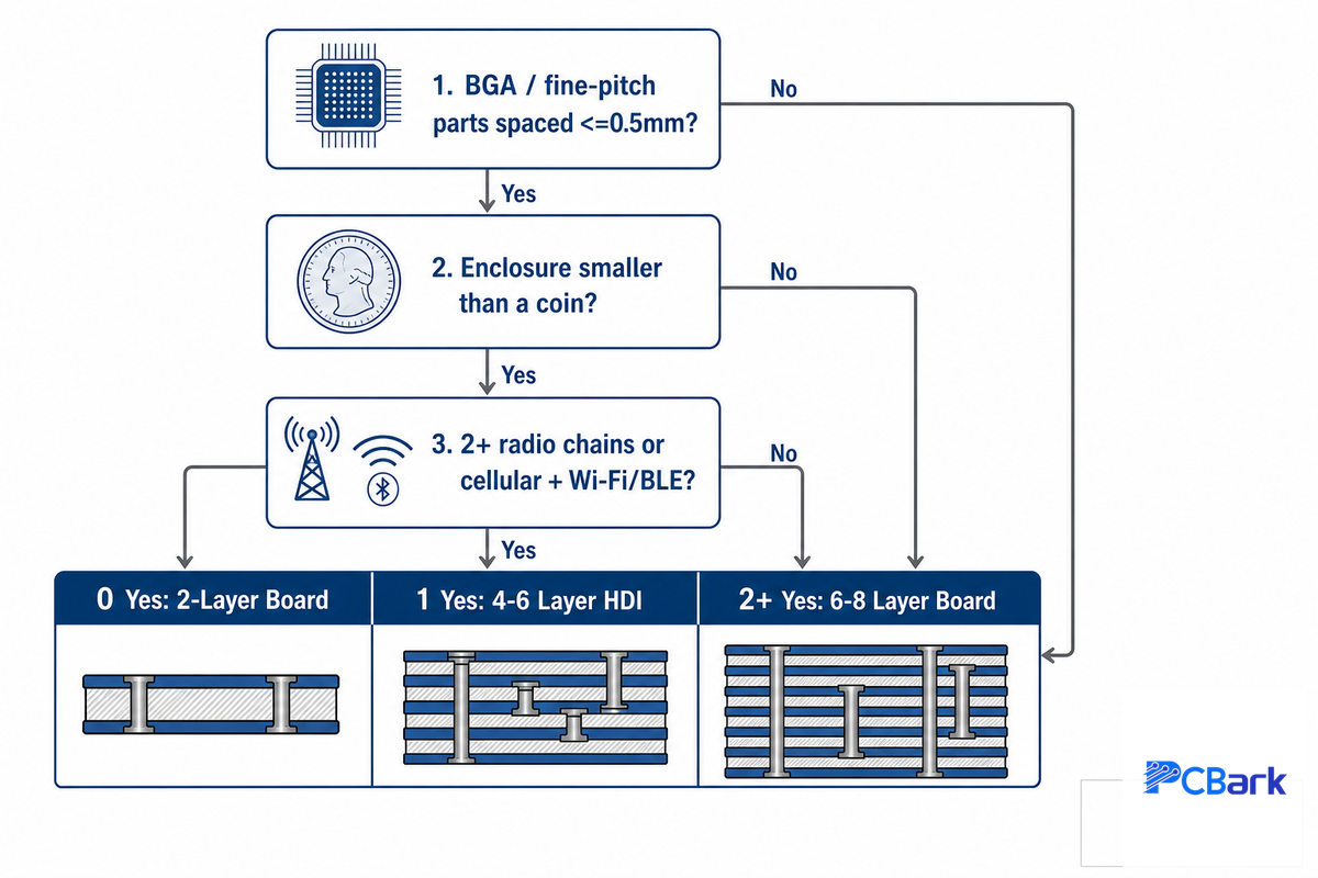
The 3 Factor HDI Decision Grid
A three-question guide to determine if you really need HDI for your design.
- Are any BGAs or fine-pitch components spaced 0.5 mm or closer? Yes. You’ll need HDI microvias (0.15mm per IPC-2226A Type I) to keep you off the pads.
- Will the enclosure force the board into less space than roughly the footprint of a coin? Yes. Try a 1+N+1 HDI buildup (an HDI layer pair surrounding a traditional core) to make space for your routing before moving to stacked vias.
- Do you’ve 2+ radio chains or need to support cellular and Wi-Fi/BLE? Yes. Those design requirements usually mandate 6-8 layers for power-integrity reasons alone, regardless of pitch.
0 “Yes”s: A 2-layer board will likely do the job. 1 “Yes” (pitch or area): A 4-6 layer HDI board is in the cards. 2+ “Yes”s, especially a “Yes” to the radio question: A 6-8 layer board, HDI or not, depending on pitch.
Failures on HDI boards tend to occur in different places than on standard multilayer boards. Via barrel fractures and outer-layer trace corrosion are the most common causes of failure on traditional multilayer boards; HDI failures, by contrast, tend to occur where the microvia joins the pad or as a micro-crack growing in the microvia, or even a gradual resistance increase due to electromigration. By controlling via aspect ratios and copper-plating thickness, HDI PCB fabrication designers can prevent this kind of failure in a manufacturable way, rather than relying on layout tricks.
📐 Engineering Note
IPC-2226A, the current version of the sectional HDI design standard, groups HDI structures by build-up type, and identifies its Type I microvia features at 0.15 mm (0.006 inches) diameter, with pad diameters below 0.35 mm (0.014 inches) and an aspect ratio at 1:1 (0.75:1 preferred for plating quality). If the design’s finest feature is above this Type I limit, the design doesn’t have to be called HDI no matter how “sophisticated”the final product may appear.
However for designs that don’t require the full HDI benefit but still require the increased routing density, a multilayer PCB stackup using simple buried vias is a lower cost intermediary solution than full stacked microvias.
Form factor constraints often push a design toward a 4-layer PCB as the practical middle ground between a simple 2-layer sensor node and an advanced PCB with a full HDI build-up. Flexible PCBs and rigid-flex constructions extend this same layer-count logic to wearable devices and other wearables and compact sensors, where thermal vias and controlled dissipation matter as much as routing density. That same production process discipline behind automotive PCB manufacturing — tight tolerance control and mature pcb technologies — carries over directly to IoT boards built on the same lines.
RF and Antenna Integration for Reliable Wireless Performance
How Important Is RF Layout in IoT PCB Design?
Antenna implementation is where IoT PCB designs most often fail in the field, rarely firmware. The 2.4GHz quarter-wave antenna length used by Wi-Fi and BLE is around 31.25mm in free space, and every trace between radio and antenna feed point must hold a strict 50-ohm match. A mismatch there reflects energy back toward the radio instead of radiating it, showing up as poor range rather than an obvious firmware bug.
The Voltage Standing Wave Ratio (VSWR) is the metric that quantifies how well matched the antenna feed actually is: the closer the VSWR is to 1 the better it’s, but once the VSWR goes above 2 the losses begin to be noticed as decreased range. That impedance is in reality set by the trace width and its height off the ground plane. In fact for a microstrip trace the impedance will decrease with increasing trace width and increase with decreased width, and laminate in the dielectric range of 3.5-4.5 (standard for most lower cost designs the cheapest 3.5 will be the FR-4, if your operating frequency is higher then look for the likes of Rogers or PTFE base laminate).
Wireless connectivity and antenna performance depend on the same layout discipline no matter which protocol you choose in the next section, and sensor integration on a shared board adds another layer of isolation requirements between the RF path and any analog measurement circuitry.
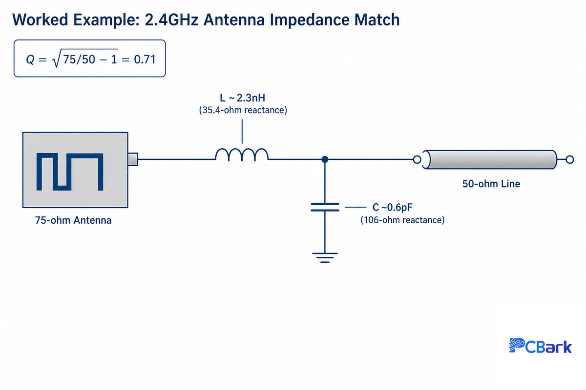
📐 Engineering Note — Worked Example: 2.4 GHz Antenna Impedance Match
Consider a practical case: a chip antenna with a native impedance of 75 ohms needs to be matched to a 50-ohm transmission line at 2.4GHz. The matching network’s loaded Q is Q = √(75/50 − 1) = 0.71. That sets a series reactance of Q × 50 = 35.4 ohms (an inductor of roughly 2.3nH at 2.4GHz) and a shunt reactance of 75 ÷ Q = 106 ohms (a capacitor of roughly 0.6pF). The exact values shift with a different antenna’s native impedance or a different frequency band, so this is a starting point for network analyzer tuning, not a universal component value.
Layout discipline matters just as much as the matching network itself. An antenna should sit at the edge or corner of the board away from the main component cluster, with all copper, ground planes and traces cleared from every layer within its keep-out zone. Don’t route high-speed digital lines close to the RF path, and the final enclosure needs to keep any metal fasteners and shielding clear of the antenna, a board that work great on a bench can still fail in the field if the enclosure design was never checked against the antenna keep-out zone. A RF PCB fabrication process that holds tight dielectric-constant tolerance across a panel is what keeps that impedance match consistent from board to board, not just on the first prototype.
Choosing a Wireless Protocol and Component Set
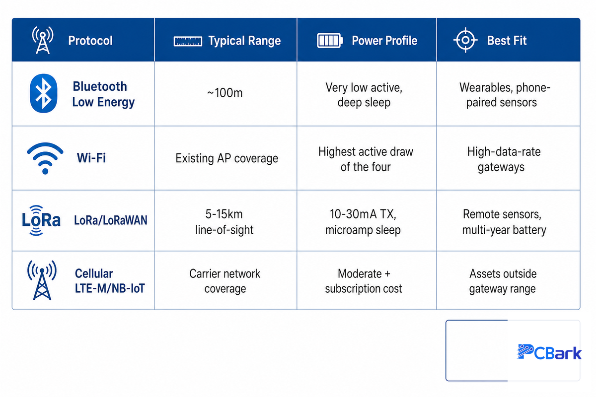
Your choice of wireless protocol determines the layout, power budget and number of layers on your board and should come first, not last. This decision is based on four things, not the radio module with which you’re most familiar: Range, power consumption, data rate and infrastructure dependency.
| Protocol | Typical Range | Power Profile | Best Fit |
|---|---|---|---|
| Bluetooth Low Energy | ~100 m | Very low active, deep sleep between beacons | Wearables, phone-paired sensors |
| Wi-Fi | Existing AP coverage | Highest active draw of the four | High-data-rate gateways, video/streaming nodes |
| LoRa / LoRaWAN | 5–15 km (line-of-sight, gateway-dependent) | 10–30 mA TX, microamp sleep | Remote sensors, multi-year battery deployments |
| Cellular (LTE-M / NB-IoT) | Carrier network coverage | Moderate, plus recurring subscription cost | Assets outside any fixed gateway’s range |
Sub-GHz LoRa devices typically work on 868MHz (Europe) or 915MHz (North America), offer small packet sizes of 51 to 241 bytes and a strict duty-cycle limitation on transmissions. These are precisely why LoRa trades data rate for range, battery life. While it won’t cut it if you need to stream constant data (don’t get it, despite the power advantage), it’s ideal for periodically sending a few readings to a server once an hour when there’s no Wi-Fi signal available. Cellular carries a recurring price point the other protocols don’t. This could matter depending on total cost of ownership, not just BOM cost.
A common mistake here is picking a protocol based on what an engineer already knows rather than the actual application: an OEM buyer sourcing a remote agricultural sensor for the field needs LoRa’s multi-year battery life, while an industrial buyer building a factory-floor gateway needs Wi-Fi’s throughput, not its power draw. Getting this wrong at the schematic stage is the single most expensive protocol decision a design team makes, because it forces a board respin rather than a firmware change once prototypes reach the field. PCBark’s turnkey DFM review, built on IATF 16949 and ISO 9001-certified process control, is specifically where this kind of protocol-to-application mismatch gets caught before tooling is committed.
One nuance worth flagging: not all Wi-Fi is short-range. IEEE 802.11ah (Wi-Fi HaLow) is an active sub-1GHz Wi-Fi amendment built for exactly this gap, supporting range up to 1km at a minimum data rate of 100Kb/s — a genuinely different profile from the 2.4/5GHz Wi-Fi most engineers default to when they hear the word. One peer-reviewed comparison in Sensors puts hard numbers on the wider LPWAN field: LoRa reaches roughly 20km range, Sigfox up to 40km, and cellular LTE-M runs up to 1Mbps with 50-100ms latency versus RedCap’s 150Mbps downlink — useful benchmarks when a design brief specifies range or throughput before a protocol has been chosen. And per 47 CFR 15.212, any pre-certified radio module still has to satisfy its own shielding, power-supply, and antenna-interface conditions to keep that certification valid in the final host design — the compliance detail covered in the hardware-security section below.
Power Management and the Power-RF-Thermal Isolation Discipline
Given that the vast majority of iot device systems will be powered by battery alone, power consumption becomes the governing parameter for the vast majority of decisions you’ll make about the PCB layout and design of your board. Achieving 1–5µA in deep-sleep, sufficient for multi-year operation on a coin-cell, means specifying a low-dropout regulator rated for greater than 90% efficiency under light loads, and verifying that every other passive component on the supply rail satisfies its specified leakage rating, not just the regulator. Low-power semiconductor design techniques of this kind, including sleep-mode current gating at the board level, are documented in patent filings such as US7282394B2 on embedded-chip power and interconnect design.
📐 Engineering Note — Worked Example: Battery-Life Estimation
The relationship for first-order battery-life calculations is quite simple: battery life (h) = Battery Capacity (mAh) / Avg. Current Draw (mA). Thus, a 220mAh coin-cell battery in a system drawing 0.01mA on average (a mixture of deep sleep and occasional burst transmits) could theoretically last 22,000 hours, or just about 2.5 years. Keep in mind this is an estimation: real-world battery life depends on temperature, discharge profile and battery cutoff voltage, among other factors, according to a recent paper on peer-reviewed battery research, so plan with margins or test using the actual cell’s discharge curve.
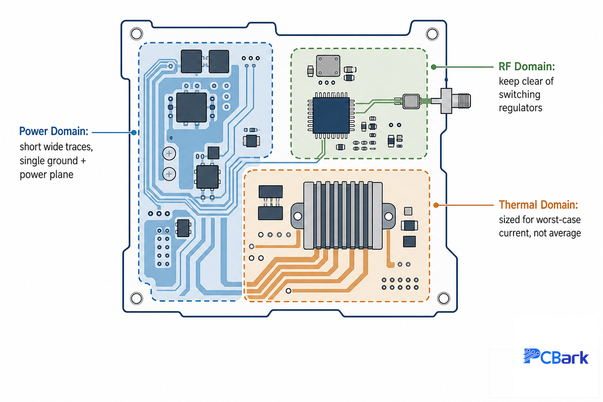
Because the two can fail together, it’s worth treating a board as consisting of three independent, though obviously related, physical domains-power, RF, and thermal-rather than as a collection of three disparate, uncoordinated, unrelated checklists.
Stable power delivery starts with routing thin power traces correctly and tying ground and power planes together without gaps between layers. Battery power budgets should account for realistic power usage patterns across a full duty cycle, not just datasheet best-case current draw — efficient power design at every stage is what separates a device that reliably lasts years from one that needs replacement within months.
The 3 Domain Power Isolation Model
- Power Domain. Power-supply traces should be short and wide to reduce resistive drop, with the board divided into a single ground plane and single power plane. Routing high-speed digital traces across a split plane is the worst offense here, creating an unpredictable loop in the return current and creates an unintended antenna that radiates noise across the board.
- RF Domain. An RF module should never be placed in proximity to a switching power regulator. Any such device injects wide-band switching noise directly into the receiver’s frontend, and nothing in the firmware will prevent it.
- Thermal Domain. Plan the thermal design to account for worst-case current draw, not average, for that reason alone. A cell transmit will put a spike of concentrated heat that would cook an adjacent analog sensor if the power and thermal copper pours were dimensioned only to the low average current flow in an IoT product.
Analog sensor circuitry needs its own isolated board sector, set aside from both high-speed digital routing and the RF section, with digital signals routed on inner layers sandwiched between ground planes to contain radiated emissions. Skipping this discipline commonly show up as voltage drop across a long, thin power-distribution trace, causing microcontroller brown-out at precisely the times the device should be functioning, for example, when associating to Wi-Fi or registering with a cellular network.
Hardware Security and Regulatory Compliance
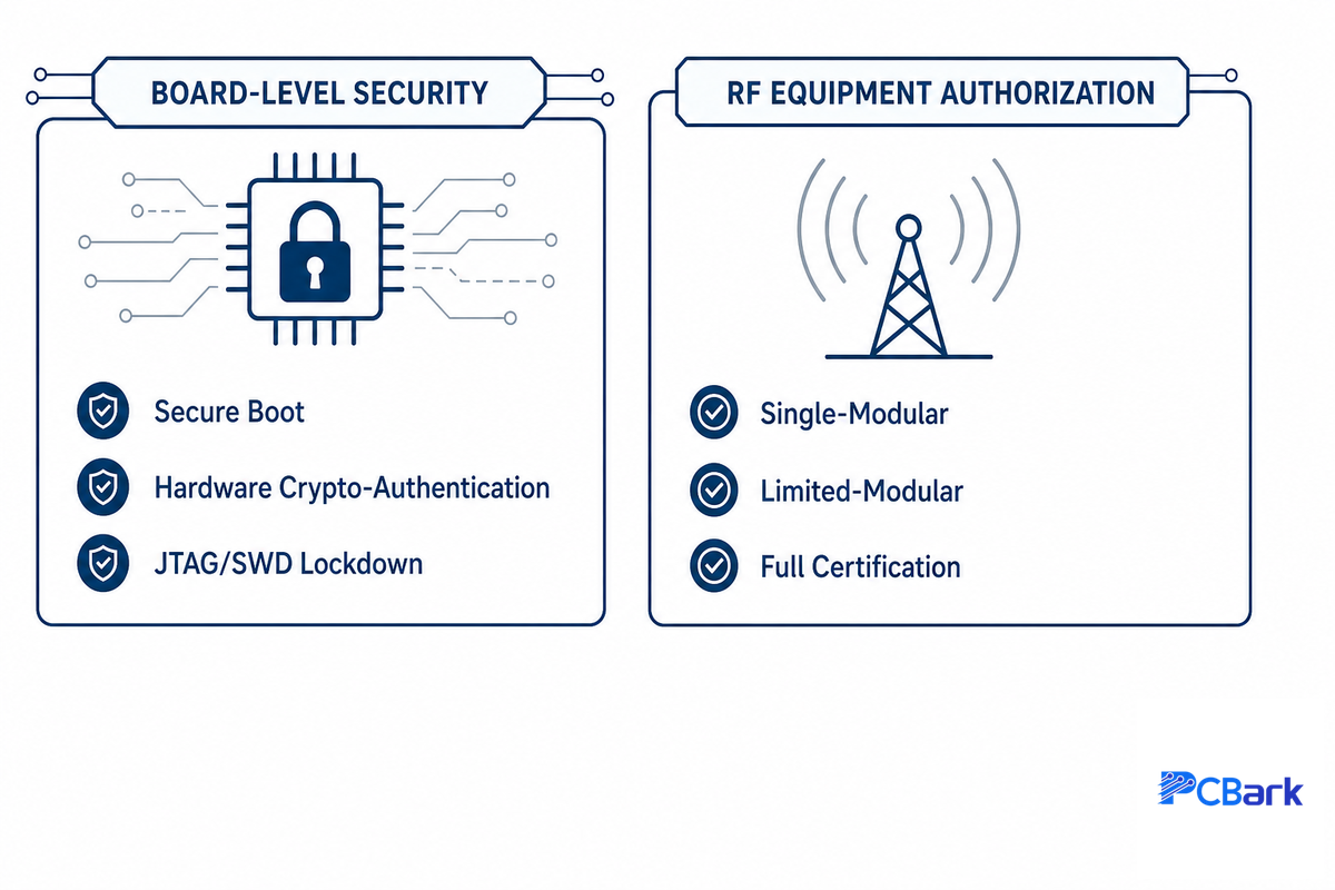
For any connected device, there are two completely different compliance disciplines, and lumping them into a single, post-design task is an easy, and expensive, mistake to make: Board level cybersecurity, and federal RF equipment authorization for the device’s radio. Neither one can substitute for the other.
Board-Level Security
Any board designer needs to allow for hardware secure boot. A JTAG or SWD port that can be used by an attacker after product delivery can be exploited to steal the device firmware, replace it with malware, and return a modified, hostile product into circulation; the physical debug-port interface must therefore be planned during the schematic stage, and not treated as something to be retro-fit in. A dedicated hardware crypto-authentication chip integrated early into the schematic provide hardware root of trust. Securing the debug port depend on the vendor: a micro controller may allow disabling JTAG/SWD through an eFuse when development is complete, or require an unlock via signed download to enable debugging, or a developer may choose not to place physical test points on the debug pads at all. Per the NIST Interagency Report 8259, Revision 1 (issued April 2026), IoT Product Manufacturer: Cybersecurity core activities should be planned into the development lifecycle as a deliberate component of the product development rather than as a post-launch patch process; a set of hardware design recommendations that apply to the foregoing board design recommendations.
RF Equipment Authorization
Having a board with a radio module in it doesn’t automatically make it FCC compliant just because the module is certified. A 2.4GHz or sub-GHz radio module will still require testing of the host: under FCC Knowledge Database guidance KDB 996369, modular transmitters require verification and testing of the final host device to demonstrate compliance, in the same way that other composite devices require testing. The modular grant simply means that the burden of testing the radio itself is lessened – the host design still needs to follow the module integration guidelines and pass a prescribed set of verification tests (including a composite test with every transmitter active simultaneously) before the product is deemed compliant. There are three types of certification based on how the module is integrated: single-modular (least host-level testing, but with strictest limitations from the module grant on layout and antenna), limited-modular, or full certification of the completed host system. This is a design-team decision that impacts everything from the need for an antenna trace vs. a connector, so it needs to be settled before laying out the antenna keep-out region described in the previous section.
Reliability and Environmental Design for Field-Deployed Devices

What Are the Biggest Reliability Risks in IoT PCBs?
iot devices endure temperature fluctuations, humidity, vibrations, and years of unattended operation that no lab bench can ever replicate, and the failures that emerge in the field are different than those found in prototypes. Especially with compact HDI IoT controllers, the root cause of field failures is typically not found in a schematic defect, but in power delivery, a failed ground plane or RF layout issue that would never surface in benign lab conditions. A documented academic field trial makes the point concretely: the UMBRELLA IoT testbed study ran 20 field-deployed devices for a six-month trial and surfaced hardware and software defects at real installation distances that lab-only validation had missed, catching them before large-scale rollout rather than after.
“In real IoT deployments, most failures do not happen in the lab, they happen months later, in the field. IoT PCBs rarely fail because of one big mistake. They fail because multiple design pressures collide on a very small board.”
A power plane/ground plane pour below any components that have high peak currents, a conformal coating rated to your specific deployment’s peak relative humidity (commonly specified around 85% RH for outdoor or industrial enclosures, though the exact figure should come from the enclosure’s environmental spec, not a default assumption), and a panelization plan that includes breakaway tabs and fiducials approved by the contracted manufacturer before release to fabrication-these are the tangible, checkable items that distinguish a prototype that works fine “on the bench” from a product that ships in the thousands and work reliably. Having a contract manufacturer perform microsection analysis and via integrity testing as part of their routine incoming inspection QC-rather than as a special order test-is what catches a failure mode of degradation at the microvias before it leaves the factory, not after units come back from the field.
Manufacturing, Assembly, and Sourcing an EMS Partner

A working prototype doesn’t say anything about whether or not a design can be mass-produced reliably. iot devices are routinely used in extreme environments that cycle through much wider ranges of temperature, humidity and vibration than a single prototype hand built on your bench, so verifying your layout choices with your contract manufacturer’s process flow before generating final Gerber files isn’t optional. If you’re building an wearable and / or miniature design that has rigid-flex elements or a non-rectangular board outline, then you need an approved breakaway tab and fiducial design that allows an automated assembler to place and process it without damaging the hanging elements.
PCBark has been offering turnkey PCB and PCBA solutions for over 16 years, providing up to 500,000 sq meters of manufacturing capacity annually that support everything from low volume HDI prototypes to volume assembly – the sort of capacity range where your DFM analysis passes are more than just a stamp. When your team is evaluating IoT-focused fabrication and assembly partners, what you really want to know from them is what HDI layer stack-up type your design decision requires, whether their certifications support the standards addressed in the next section, and whether they’ve a genuine capability for low volume or prototype runs without forcing you to buy a full volume run before your product is ready. With PCBs from prototypes through production that pass true HDI testing and provide certified volume assembly, PCBark’s iot pcb manufacturing services offer a one stop path.
Manufacturing and assembly capability covers the full pcb design and manufacturing lifecycle — design and manufacturing coordination during DFM review, through pcb manufacturing and assembly at volume. Working with pcb manufacturers who understand automated assembly constraints for high-performance iot devices, and who can deliver reliable iot pcbs at volume and not just on a prototype run, is what determines whether a design survives the jump from bench to production. The right circuit components and a production process built for both common pcb builds and effective pcb builds alike matter here just as much as sourcing pcbs for iot programs from a single accountable partner.
Request an IoT PCB Quote →
Ask About HDI Prototype Runs
Quality and Certification Standards for IoT PCBA
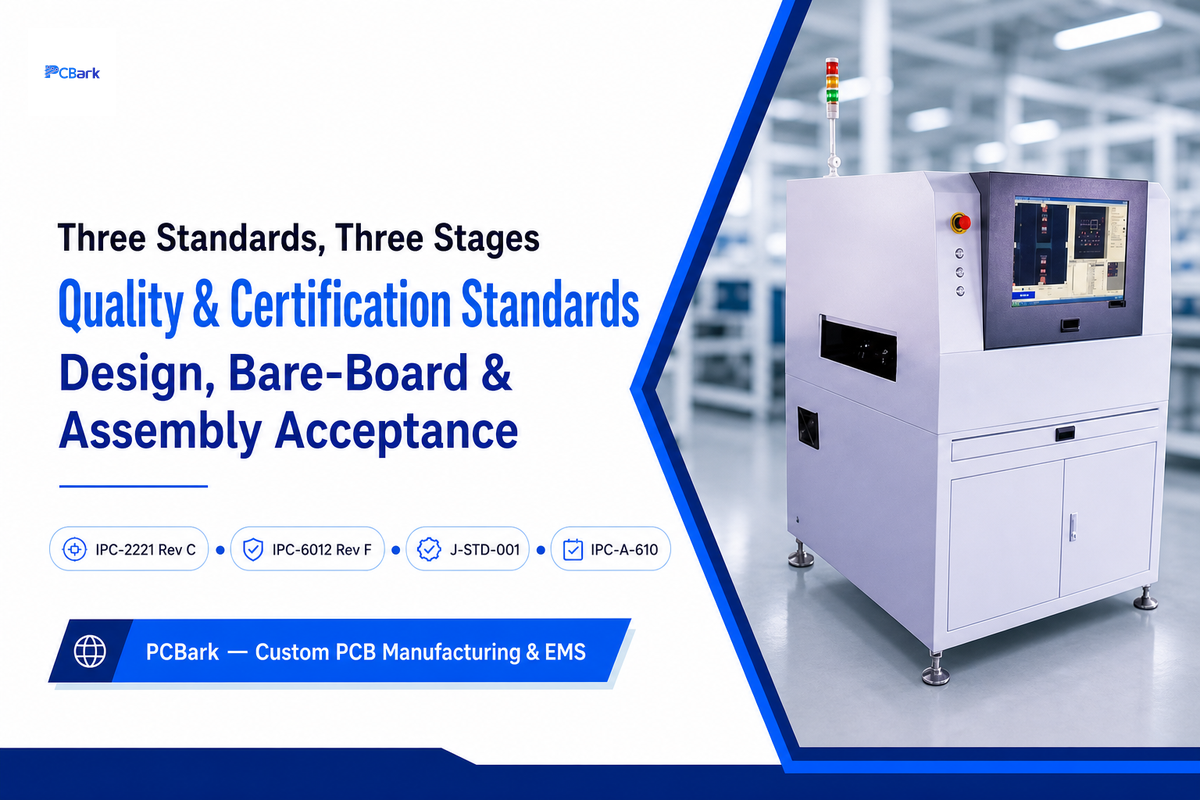
Be warned: “IPC certified” doesn’t refer to any single, all-encompassing standard; there are actually three distinct standard families that correspond to the three key phases of taking a board from a schematic through to an assembled product and so the particular IPC standard that your potential supplier refers to can make a big difference when you’re placing your PO. NASA’s GSFC-STD-8001 quality-assurance requirements for printed circuit boards illustrate just how granular this scoping gets in a high-reliability program, breaking design, fabrication, and assembly acceptance into separate qualification stages.
| Standard | Governs | Applies At |
|---|---|---|
| IPC-2221 (Rev C) | Design rules: material selection, conductor spacing, clearance, via design, thermal management | Design phase, before fabrication |
| IPC-6012 (Rev F) | Bare-board qualification: structural integrity, solderability, conductor spacing on the fabricated board | After fabrication, before assembly |
| J-STD-001 / IPC-A-610 | Assembly and soldering acceptance criteria for the populated board | After assembly, final acceptance |
IPC-2221 specifies design standards for layout; IPC-6012 provides standards for acceptance of bare PCBs (pre-populated); J-STD-001 along with IPC-A-610 cover acceptance criteria for soldered, assembled boards. Simply saying your product meets “IPC certified” may not mean anything as for some board and connector systems your interconnects will need to meet IPC/WHMA-A-620 for those cable-and-wiring components; also the certification requirements for acceptance of bare PCBs (IPC-6012) will be unrelated to the workmanship of soldering that goes on when you bring components onto your boards (J-STD-001 and IPC-A-610).
With a design that’s getting so far out in terms of routing density as to border on the HDI it actually is. In the case of the IPC-2226A, the aforementioned sectional HDI design standard simply adds microvia design requirements on top of the more general requirements of IPC-2221. It’s not a standalone design standard in this respect, it’s an additive standard that defines a section of a design.
Common IoT PCB Design Mistakes to Avoid
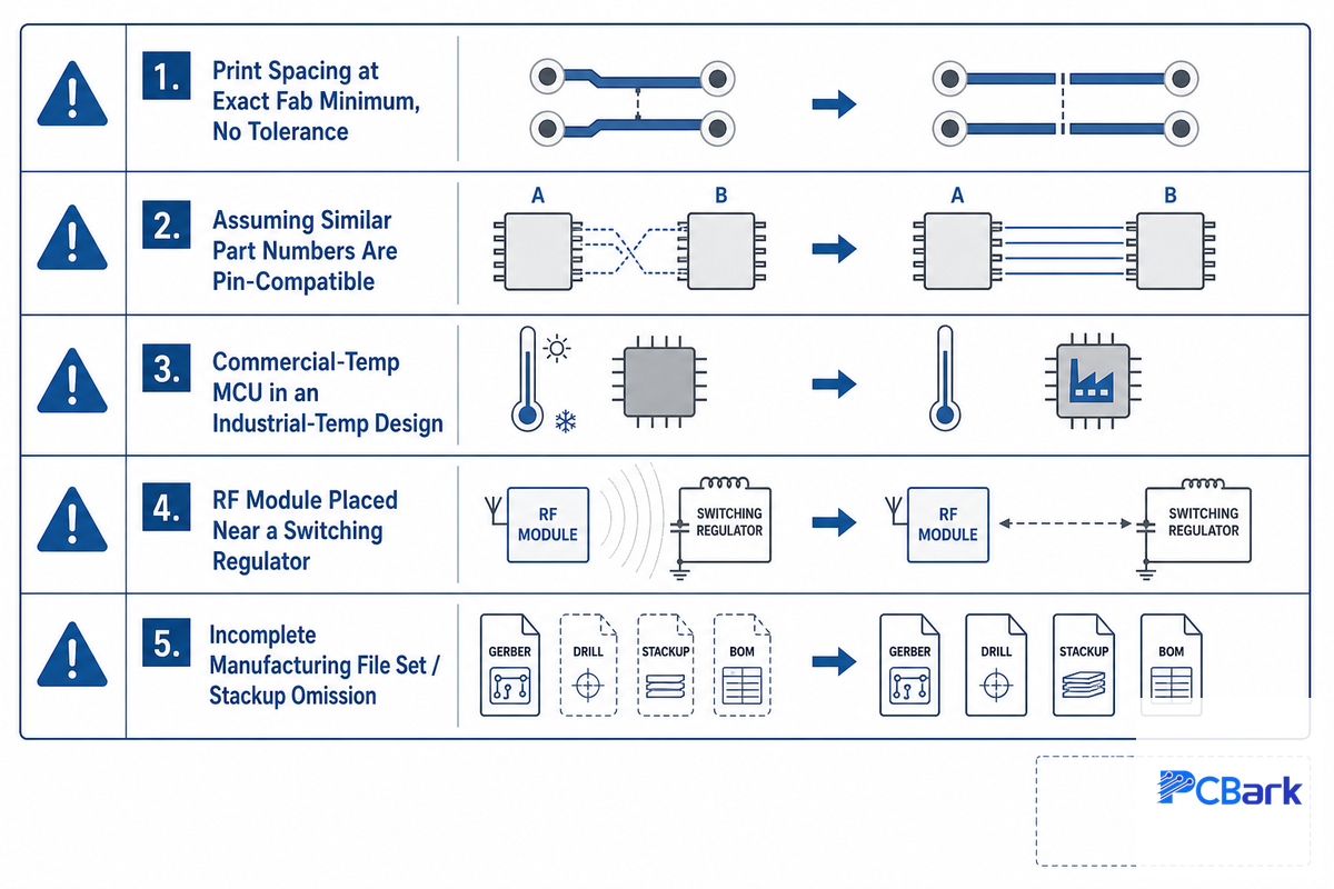
Two separate design-guidance authors agree on a short list of field-tested mistakes, a much stronger indicator of common pitfalls than either individual article is.
- Print spacing of exactly the fab’s minimum (e.g., 0.10mm), no room for tolerance — actual etch will often erode the spacing to 0.06mm in fabrication, on standard 1oz copper etch factors, creating shorts where none were in the design file.
- However, wrongly assuming that two components with similar part numbers are pin compatible is a real risk: a substitute LDO regulator with an inverted enable-pin polarity has been known, in practice, to cause prototype power-up failure.
- Choosing a commercial-temperature-rated MCU (0–70°C, a 70°C window) for a design that will indeed run over an industrial temp range (−40 to 85°C, a 125°C window)-the difference that reveals itself as thermal throttle, or worse, system death during environmental validation-but not during board level, room temperature testing.
- (The above and placing an RF module in the close proximity to the switching regulator, dumping broadband noise straight into the receiver front end, which we discuss further in the isolation-discipline section earlier)
- Sending out the manufacturing file set with an omission for an unexplained stackup or tolerance in the fabricator’s hands, and you’ve turned an easy documentation error into an even easier production one.
None of those are exotic failure modes. Those are the concrete, inspectable points that a design review ought to explicitly step through prior to shipping a board out to fabrication — not a vague “make sure the design is sound”, but rather a list of the five actual failure points discovered through field data for IoT boards. Best practices for pcb design for IoT devices increasingly mean checking against this kind of real field data, not just a datasheet checklist — the same discipline documented in manufacturing-sequence patents like US Patent 12,063,751, where repeatable, fully specified process steps are what separates a design that scales from one that doesn’t.
Industry Outlook: What’s Changing in IoT PCB Manufacturing
The most obvious near-term change in iot pcb sourcing isn’t a market-size number – it’s that HDI and miniaturization techniques that once were reserved for the consumer’s finest electronics are now table stakes for an even larger range of iot device classes — from the consumer ones down through the industrial and automotive adjacent ones that would have once run on standard multilayer boards. EE Times’ trade coverage highlights IoT in particular as one of the acceleration trends pushing up PCB demand, for precisely the reason that designing for IoT requires solving for the sensors, the power circuitry, and the wireless communication together, as a system, rather than in their discrete pieces–precisely the discipline this guide walked you through step by step. Growing demand for IoT applications across devices and technologies of every kind, from wearables and compact sensors through automotive PCB integrations, is one driver behind the broader considerations for IoT that manufacturers are weighing today. So if you’re thinking about what to do for your 2026 or 2027 program, then what it implies for your planning is that the ability to execute HDI and the process-level discipline in DFM of your manufacturer are now important to a larger swath of your IoT designs than was the case even a year or two ago, and not just those that go in the latest top-end wearable. That HDI-capability expectation is increasingly paired with the cybersecurity planning covered earlier in this guide (NIST IR 8259 Rev.1), since both are now treated as baseline procurement criteria rather than optional add-ons for a 2026-era IoT program.
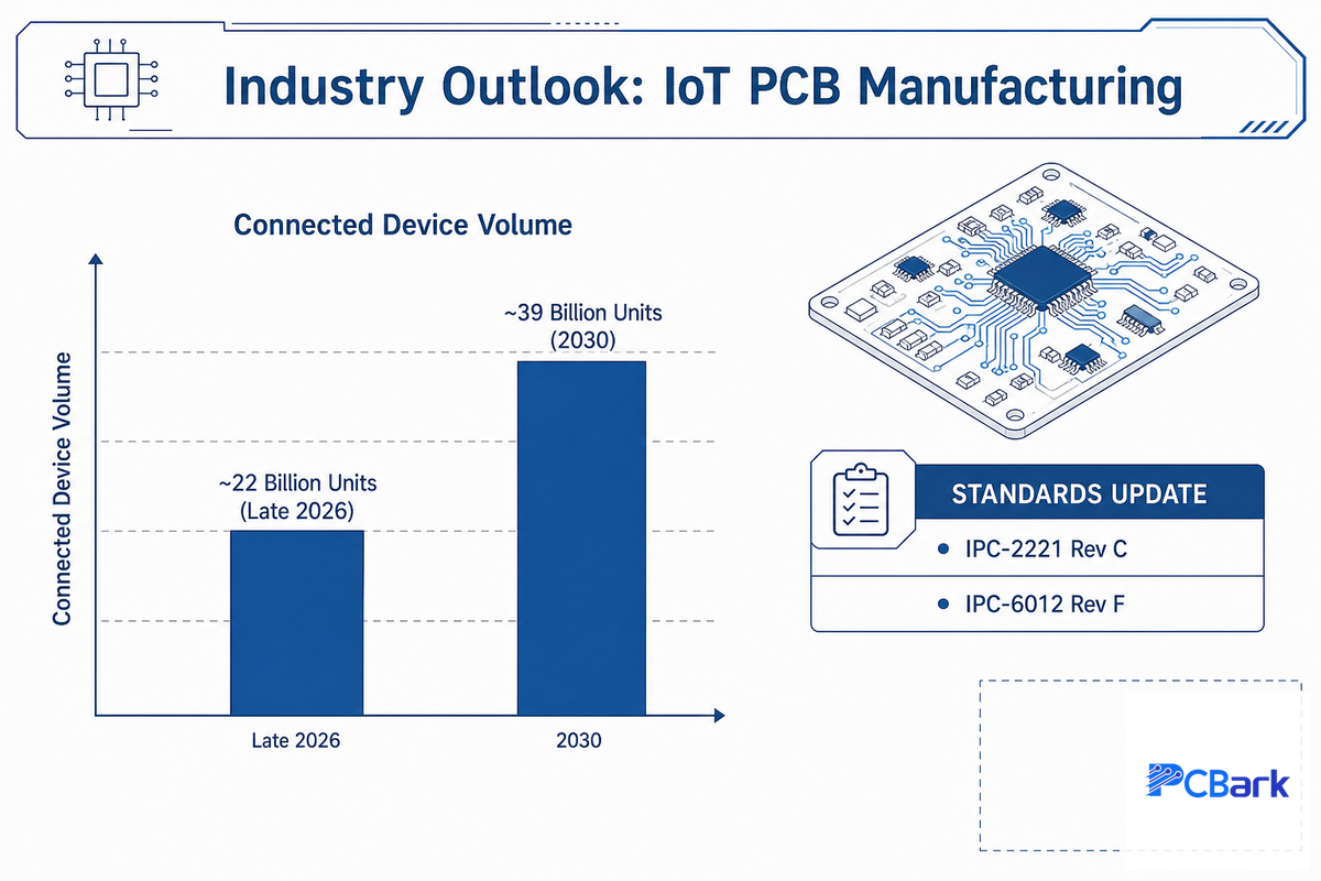
In standards, both IPC-2221 (now at Rev C) and IPC-6012 (now at Rev F) have received significant updates — new guidance on material/copper foil selection, edge-board plating and, in particular, microvia reliability criteria in 6012F — that merit close attention from any team who defaults to the existing, or an older, revision out of habit. Such a revision change can be substantial; microvia reliability guidance in 6012F, for example, is directly applicable to any HDI-designed IoT device.
Industry-wide projections suggest that connected device volume will increase from ~22 billion units in late 2026 to about 39 billion in 2030. Knowing this directional trend can help teams think long-term about product roadmap decisions, but it says nothing specific about which board designs or material selections a program should make for a next-generation device. It’s the standard and HDI-adoption trends above that actually change what a design team need to do from one year to the next.
Design teams face a structural risk here, not a hypothetical one: assuming an existing FR4 fabricator’s certification automatically covers HDI microvia builds is a common and expensive gap, because IPC-6012F’s newer microvia reliability requirements are unfamiliar territory for suppliers built around conventional multilayer boards over the past 10 years. PCBark’s HDI and conventional production lines share the same in-house, ISO 9001-certified process control, which is what closes that gap for an OEM buyer evaluating a single manufacturing partner across both build types in the field.
Frequently Asked Questions
Q: What Is an IoT PCB?
View Answer
An iot pcb integrates a radio, a microcontroller, and one or more sensors into a tiny, efficient package, optimized specifically for four factors simultaneously: miniaturization, ultra-low power consumption for battery life, maintaining RF signal integrity at extremely close component spacings, and guaranteeing long-term reliability in the harsh and variable conditions typically found in field operation.
Q: What Is HDI in IoT PCB Design, and Do All IoT Devices Need It?
View Answer
High-Density Interconnect (HDI) uses microvias, blind/buried vias, and fine-pitch routing to pack denser interconnect into the same board area, defined under IPC-2226A Type I as microvias ≤0.15mm with pad diameters under 0.35mm and an aspect ratio capped at 1:1. Not every IoT device needs it: simple, low-complexity sensor nodes work fine on basic two-layer boards. HDI earns its cost premium specifically when BGA pitch drops to 0.5mm or below, or when enclosure size won’t allow standard component placement.
Q: Can IoT PCBs Be Designed for Low-Volume or Prototype Production?
View Answer
In most cases, the answer is yes; the trick is to find a contract manufacturer who can accommodate those low-volume, true-prototype runs without forcing a large minimum production order quantity on a design before it’s validated. Contract manufacturers who are capable of producing both HDI prototypes and high-volume runs on the same production equipment often pass design-for-manufacturability lessons directly from one phase to the next, resulting in fewer and faster design-build cycles.
Q: What IPC Standards Apply to IoT PCB Assembly?
View Answer
Assembly and soldering workmanship is governed by J-STD-001 and IPC-A-610, not IPC-6012 (bare-board fabrication) or IPC-2221 (design rules) — naming the wrong one on a purchase order is a common, costly mix-up. Cable-and-wiring interconnects also fall under IPC/WHMA-A-620.
Q: What Type of PCB Is Best for a Given IoT Device?
View Answer
Device class, not a universal answer: a simple sensor fits 2 layers, a Wi-Fi/BLE gateway needs 4-6 layers, and a multi-radio cellular gateway often needs 8 or more layers for power-integrity reasons alone, not because of routing density.
Q: How Do IoT PCBs Differ From Standard PCBs?
View Answer
A standard PCB only needs to be functionally capable; an IoT PCB has to meet that function while also holding controlled RF impedance, running on microamp sleep currents for years of battery life, surviving field conditions beyond a lab bench, and, if it carries a radio module, clearing a separate FCC authorization track alongside any IPC quality standard — all at once, on a smaller board.
Why We Write This
The intention behind writing this guide is to tease apart the critical load-bearing engineering choices (layer count, RF impedance, choice of standards) that define IoT pcb design, from common “rules of thumb” repeated without critical review (like assuming HDI is the only path forward). We produce high-volume, conventional multi-layer, and HDI IoT PCBs at PCBark, so the recommendations here come from our perspective as manufacturers with significant DFM experience. Reviewed by the PCBark technical team.
References & Sources
- NIST Interagency Report 8259 Revision 1: Foundational Cybersecurity Activities for IoT Product ManufacturersNational Institute of Standards and Technology (finalized April 2026)
- GSFC-STD-8001: Standard Quality Assurance Requirements for Printed Circuit BoardsNASA Goddard Space Flight Center
- KDB 996369: Modular Transmitter Approval GuidanceFederal Communications Commission, Office of Engineering and Technology
- IPC Releases J-Revisions of Two Leading Standards for Electronics Assembly (J-STD-001 / IPC-A-610)IPC / Global Electronics Association
- IPC Standards Revision TableGlobal Electronics Association (confirms current IPC-2221 Rev C and IPC-6012 Rev F)
- IPC-2226A: Sectional Design Standard for High Density Interconnect (HDI) Printed BoardsGlobal Electronics Association
- US Patent 12,063,751: Manufacturing Sequences for High Density Interconnect Printed Circuit BoardsUnited States Patent and Trademark Office
- Trends and Challenges in PCB ManufacturingEE Times
- The 50 Ω Question: Impedance Matching in RF DesignAll About Circuits
Related Articles
- Ceramic PCB Guidematerials science and manufacturing process for high-thermal-conductivity substrates
- Aluminum PCB Guidemetal-core PCB design for thermal-management-critical applications
- Turnkey PCB Assembly Guideend-to-end sourcing from bare board through populated assembly
- Industrial Control PCB Guidedesign considerations for harsh-environment industrial deployments
- PCBark IoT PCB Manufacturing Servicescapability matrix and turnkey EMS solutions for connected-device programs