Get in touch with PCBark Company

HDI vs MLB
HDI PCB vs Multilayer PCB: When You Actually Need HDI
Both technologies stack copper to route dense designs. The real engineering question is not which board is “better” – it is the point at which your part count, BGA pitch, and signal speed can no longer fit on a traditional multilayer board.
Get a Free DFM Review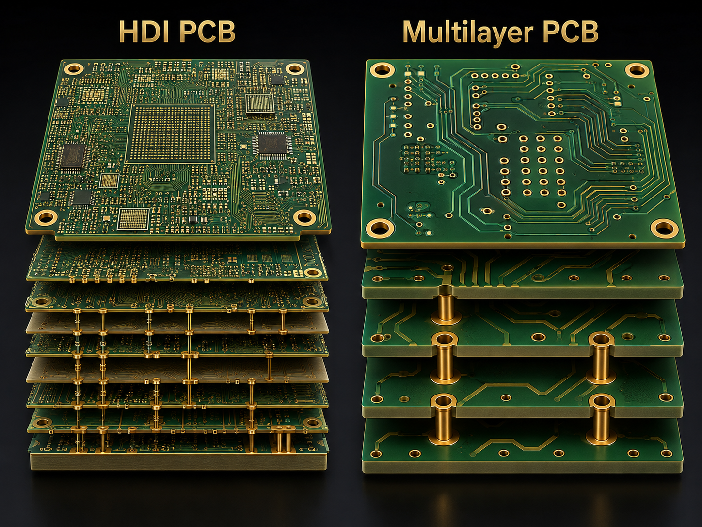
Side-by-side, by the numbers
≤0.5 mm
BGA pitch that typically forces HDI
<150 µm
Typical microvia diameter
1+N+1 → any-layer
HDI build types we run
IPC Class 2/3
Build standards offered
16 yrs
PCBark fabrication experience
Engineering Reference
When You Need HDI — A Decision Matrix
We get asked all the time about the difference between traditional multilayer boards and their high-density interconnect (HDI) counterparts. Most comparison guides leave you with little more than a general understanding of what HDI offers over multilayer designs – smaller components, more traces per square inch, and perhaps a touch better performance. This guide tells you more – it describes the points at which you really have no choice but to transition from a multilayer PCB to HDI design. When those points arise, here are the exact limits we apply at the incoming DFM stage to decide whether a design truly necessitates the additional complexity of HDI technology.
In practice these triggers cluster in the same products — smartphone main boards, 5G and RF modules, automotive ADAS sensor modules, and compact wearables — where board area is scarce and signal speed is high. Industrial and power electronics rarely hit them.
| Design trigger | Threshold (rule of thumb) | Verdict |
|---|---|---|
| 01Fine-pitch BGA / CSP escape routing | Pitch ≤ ~0.5 mm, or high I/O count | HDI required (microvia / via-in-pad) |
| 02Trace width / spacing demand | Need < ~100 µm lines | HDI required |
| 03Layer count vs. space / weight budget | Layer count won’t fit board area or thickness | HDI (any-layer can cut layers) |
| 04High-speed / RF signal integrity | Need short, controlled-impedance paths, low crosstalk | HDI favored (microvia stubs shorter) |
| 05Product form factor | Wearable, handset, implant, dense module | HDI favored |
| 06Coarse components, ample space | ≥ 0.65 mm pitch, moderate density | Standard multilayer is enough |
| 07Cost-driven, high-volume, simple routing | Density well within PTH capability | Standard multilayer is cheaper |
Engineering Note
Why 0.5 mm Pitch Is the Wall
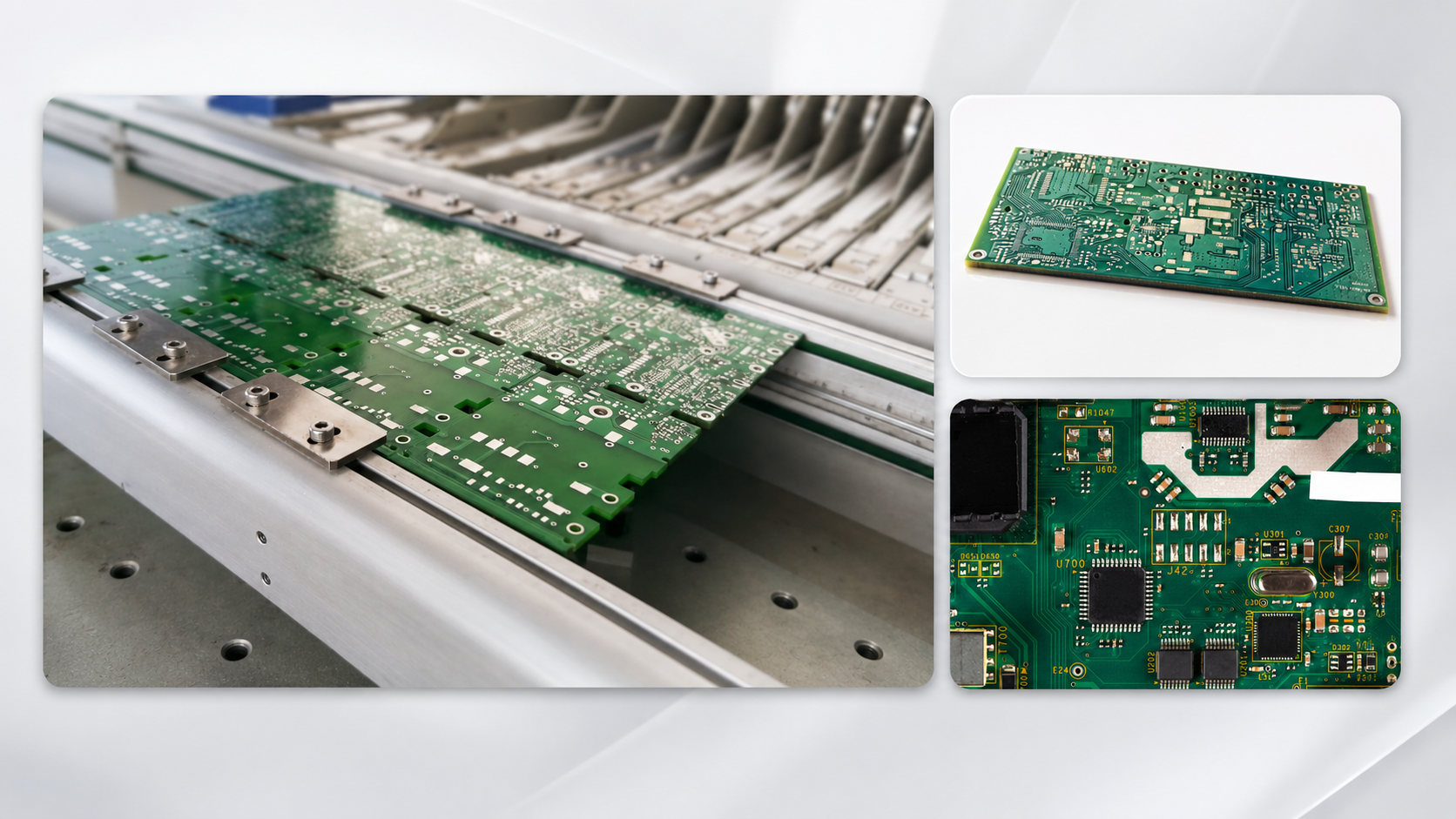
Below approximately 0.5 mm BGA pitch there simply isn’t enough space between adjoining pads for a via and its antipad plus an escape trace. A microvia placed directly in the pad (via-in-pad), filled and plated over, is the only fix here — and only HDI processing can do it. This, alone, is the actual reason for the “HDI required” judgement; it is geometric constraint, not a designer’s whim. This reasoning also applies to a greater or lesser extent as I/O increases: a 600+ ball device at 0.8mm pitch is often quite capable of running out of viable via options before it runs out of escape width even though it seems fine at first blush.
Build Strategy
When Standard Multilayer Is the Smarter Choice
This deserves to be said plainly, since nobody else in the industry will: HDI is not necessarily the most appropriate choice. In fact, for many of your industrial, power, and control electronic boards, the economical and efficient choice is simply a multilayer board. If your best-case pitch is a 0.8mm QFP and your clock speed tops out a moderate data bus and your layout isn’t even half-full, you’re getting nothing but cost and risk by using HDI.
01Hybrid Build
HDI Outer Layers Over a Conventional Core
Yet another choice, invisible in a pure “HDI vs. multilayer” box, exists: a hybrid build — HDI structures on the outer layer pairs over a conventional multilayer core. This lets you escape-route one dense BGA without paying for any-layer construction across the whole board, and without adding board thickness. For teams migrating a maturing product toward higher density, it is usually the cost-controlled first step, and the route we most often recommend on a first HDI project.
02Sourcing Advisory
Don’t Over-Specify
One source of the price “bleed” we see in new RFQs is a fully specified “any-layer” HDI stack-up on a board that only contains one fine-pitch part. Check with your fabricator what the layer pairs actually need (before signing a committed build type) – reserving HDI for the pairs that genuinely need it – and letting the other ones be conventional multilayered, for instance, can shave a surprising chunk off the price, with zero changes in the schematic.

Cost Analysis
The Cost Question — Total Cost, Not Just Board Price
“Well, how much more for HDI?” is how the procurement call always starts, and the honest, initial answer is: a little more per square foot. The addition of laser drill and sequential lamination add additional steps and thus lead to added time and cost. However, this is a poor way to begin comparing options, because the bare-board price matters far less than the number that actually lands in your Bill of Materials.
HDI’s play is layer reduction and miniaturization. By eliminating free routing, a design that might require a huge conventional layer count can sometimes fit in just a few HDI layers, in a smaller board. Fewer layers, smaller size, a much thinner board, and higher yields on fine pitch components can compensate for the increased layer cost, provided we have reached a certain density. Otherwise, the conventional board will simply be less expensive.
The Crossover Principle
Total cost ≠ board price
The HDI cost crossover depends on layer reduction, panel utilization, and assembly yield — evaluate it per design, not per square inch.
- Layer reduction
- Panel utilization
- Assembly yield
Qualitative cost model — based on standard PCB cost drivers (process steps, layer count, panel area). Not a guaranteed figure; request a costed comparison for your build.
Quote Both Constructions Before You Commit
A sensible move is to quote each construction approach on the same design before you commit. Your fabricator should be able to tell you where the crossover sits for your board — and whether a hybrid build wins on both cost and signal integrity. That side-by-side comparison is exactly what our DFM review produces.
Build Types & Stack-ups
HDI Build Types & Stack-ups — 1+N+1, 2+N+2, Any-Layer
“HDI” isn’t one construction — it’s a range of stack-ups, classified by how many sequentially laminated microvia layers sit on each side of a conventional core. Picking the right HDI PCB build is most of the cost-versus-capability trade-off.
The common build types
1+N+1
01
Structure
One microvia layer each side of an N-layer core
Best fit
Single fine-pitch BGA, entry-level HDI
2+N+2
02
Structure
Two sequential microvia layers each side
Best fit
Denser routing, stacked/staggered vias
Any-layer
03
Structure
Microvias on every layer, no through-holes
Best fit
Highest density — handsets, modules
Engineering Note
Stacked vs. Staggered & the Aspect Ratio Limit
A blind via or microvia links only the layers it must, never the entire board. On a 2+N+2 or any-layer build you route those microvias across layers either stacked (directly on top of one another, copper-filled) or staggered (landing on a pad between). Stacked vias route tighter but depend on reliable copper fill, which adds cost; staggered vias are more forgiving but consume board area. A second blind via stacked on the first has to register precisely, or yield drops. Stacked microvias also run up against a practical depth-to-diameter limit, which is why HDI boards are built layer by layer rather than drilled in one pass. Registration tolerance between sequential laminations is the quiet driver of HDI yield — the line between a clean board and a field failure. These boards are qualified to IPC-6012, with Class 3 reserved for high-reliability uses.
Manufacturing
How PCBark Builds Both — DFM-First, Prototype to Volume
Regardless of whether your choice places you on one side of the argument, the board is built at PCBark; be it a traditional multilayer, 1+N+1, to all layer,HDI, or anything in the middlehybrid. Electronic manufacturing solutions since 2005, our facility processes half million m per year, and when your board is built at PCBark, we deal with it from the position of an integral component within your complete unit, not a standalone item.
How that looks in practice: proactive DFM on every job – it’s that same engineering thinking that informs the matrix we referenced above – so you see your structures, aspect ratios, and registration tolerances before you tooling not after a bad first article. Then it’s truly turnkey: sourced components (you get our pricing), fabrication, precision SMT, and in-process inspection – all done here, in one location. From prototype for a quick turn, to higher volumes, we scale our builds with no supplier re-qual.
Turnkey, One Location
One Facility, End to End // no supplier re-qual
02
Component Sourcing
Sourced components at our pricing
03
Fabrication
Multilayer, HDI & hybrid builds in-house
04
Precision SMT
Fine-pitch assembly under one roof
05
In-Process Inspection
Quality verified at every stage
Since 2005 — half a million m² processed per year. From prototype quick-turn to higher volumes, builds scale with no supplier re-qualification.
What to Send Us for an Accurate HDI Quote
Five things
01
Gerber files or ODB++
02
Target stack-up (the “advise”)
03
Your smallest BGA pitch
04
Tightest impedance tolerance
05
Your targeted volume
Gerber files or ODB++, target stack-up (the “advise”), your smallest BGA pitch, the best possible tight tolerance on impedance, and what your targeted volume looks like. Once we know those five things, we can simultaneously quote a classic multi-layer, HDI and offer one of our high-value hybrid options; and then show you exactly where your price crossover begins.
Quality & Compliance
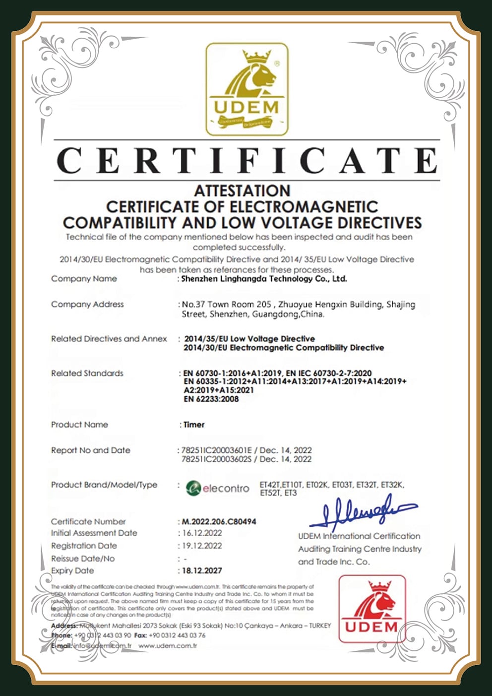
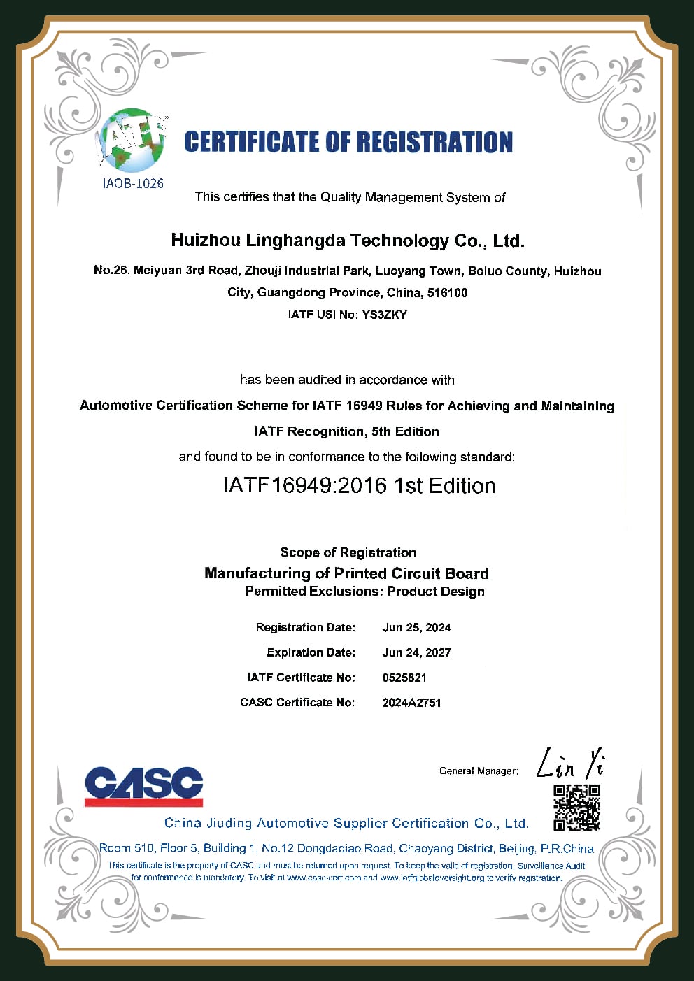
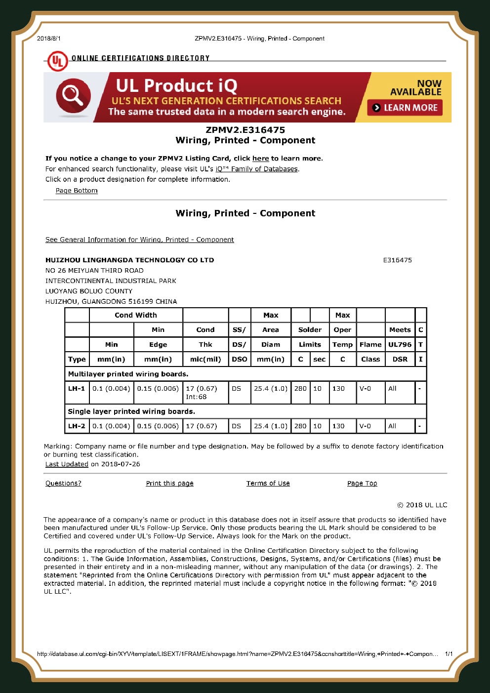
Certifications & Standards
08 accredited standards
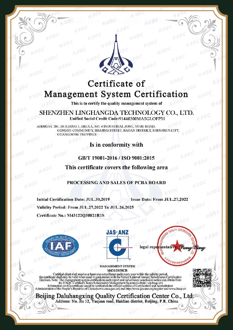
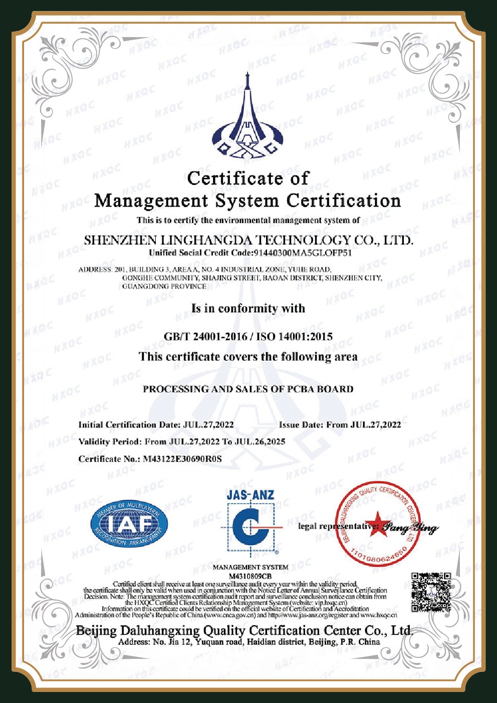
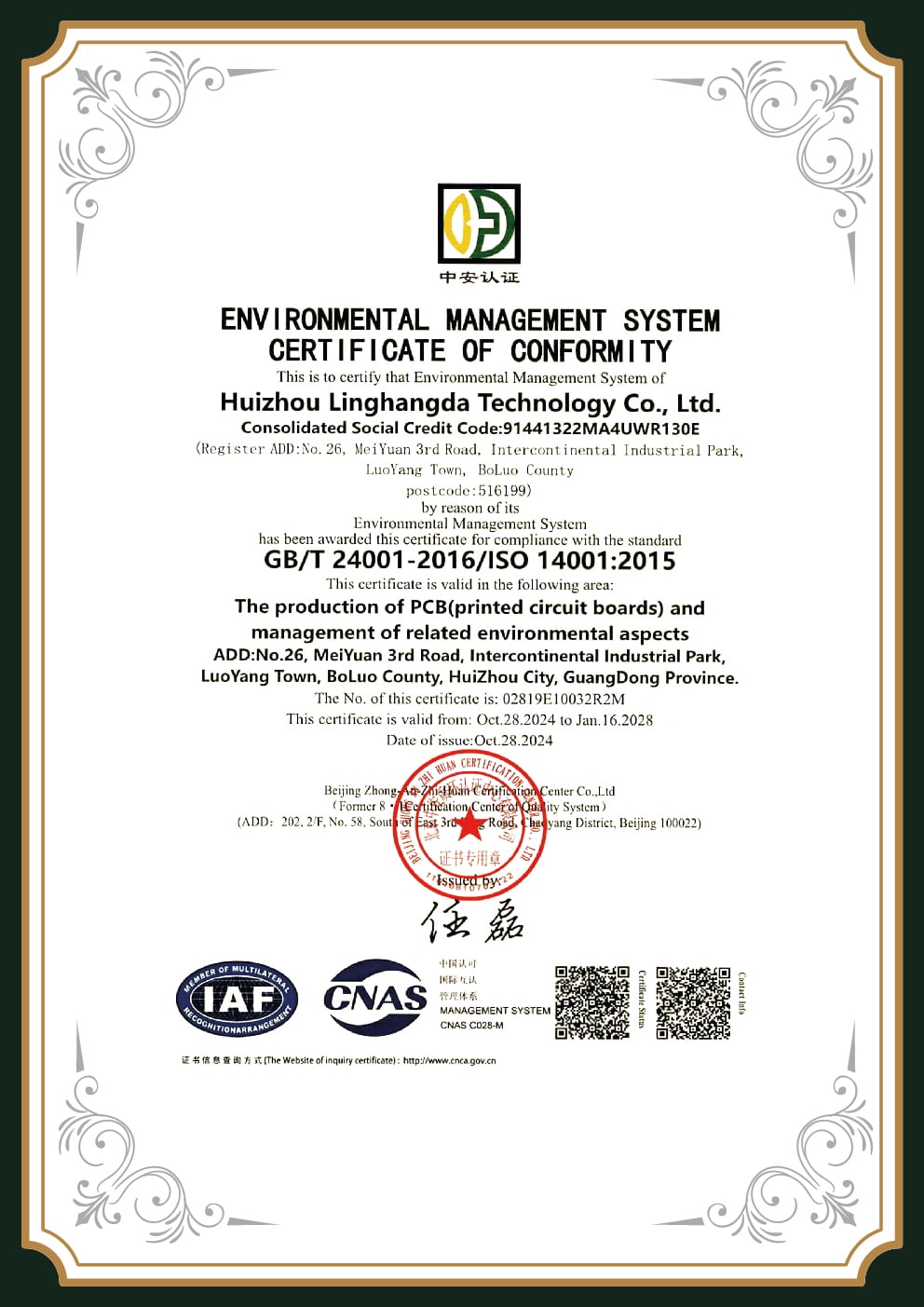

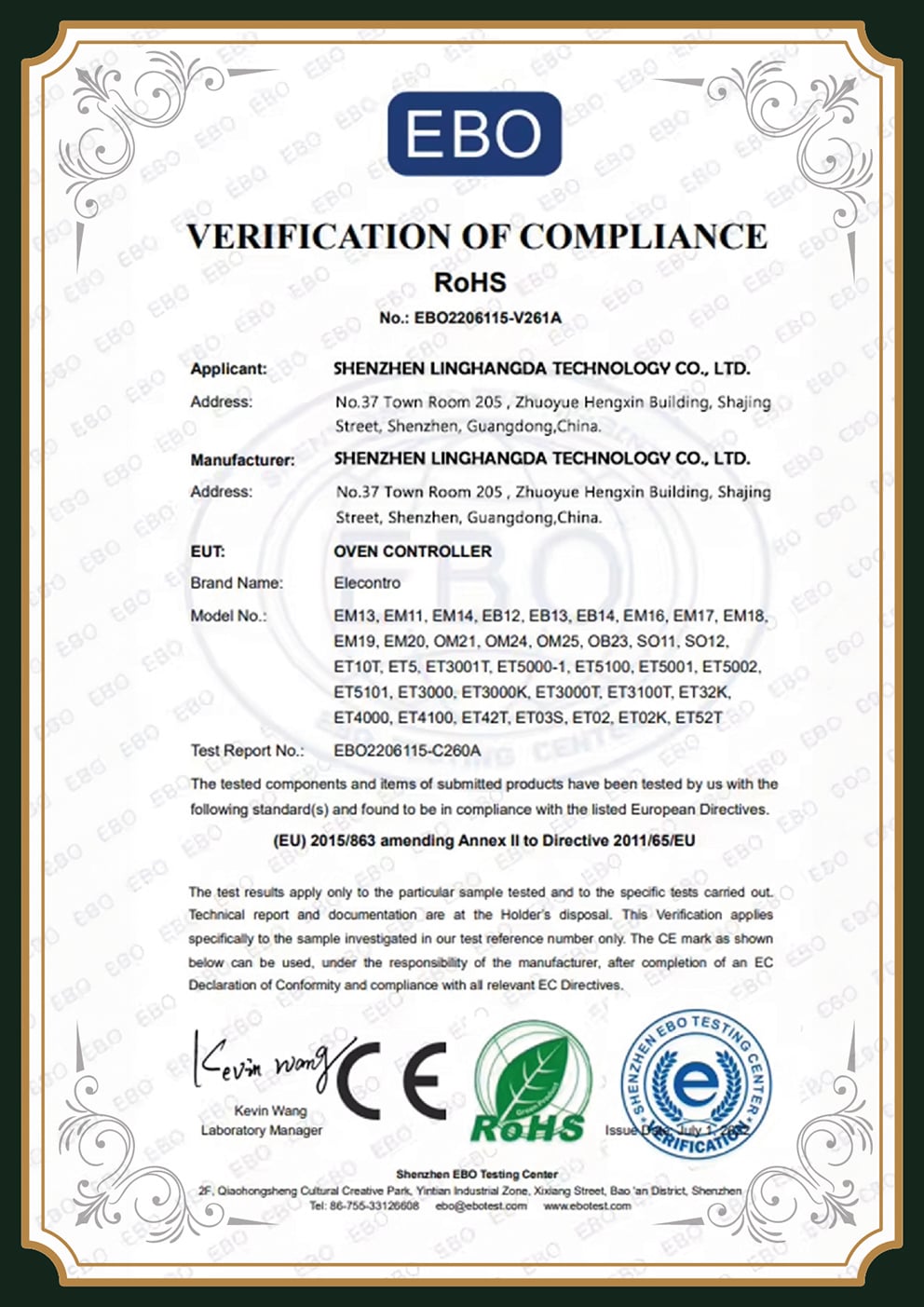
FAQ
HDI vs Multilayer PCB — FAQ
07 QUESTIONS
The questions our DFM engineers field most. Tap any question to expand the answer.
01
What is the difference between HDI and a standard multilayer PCB?
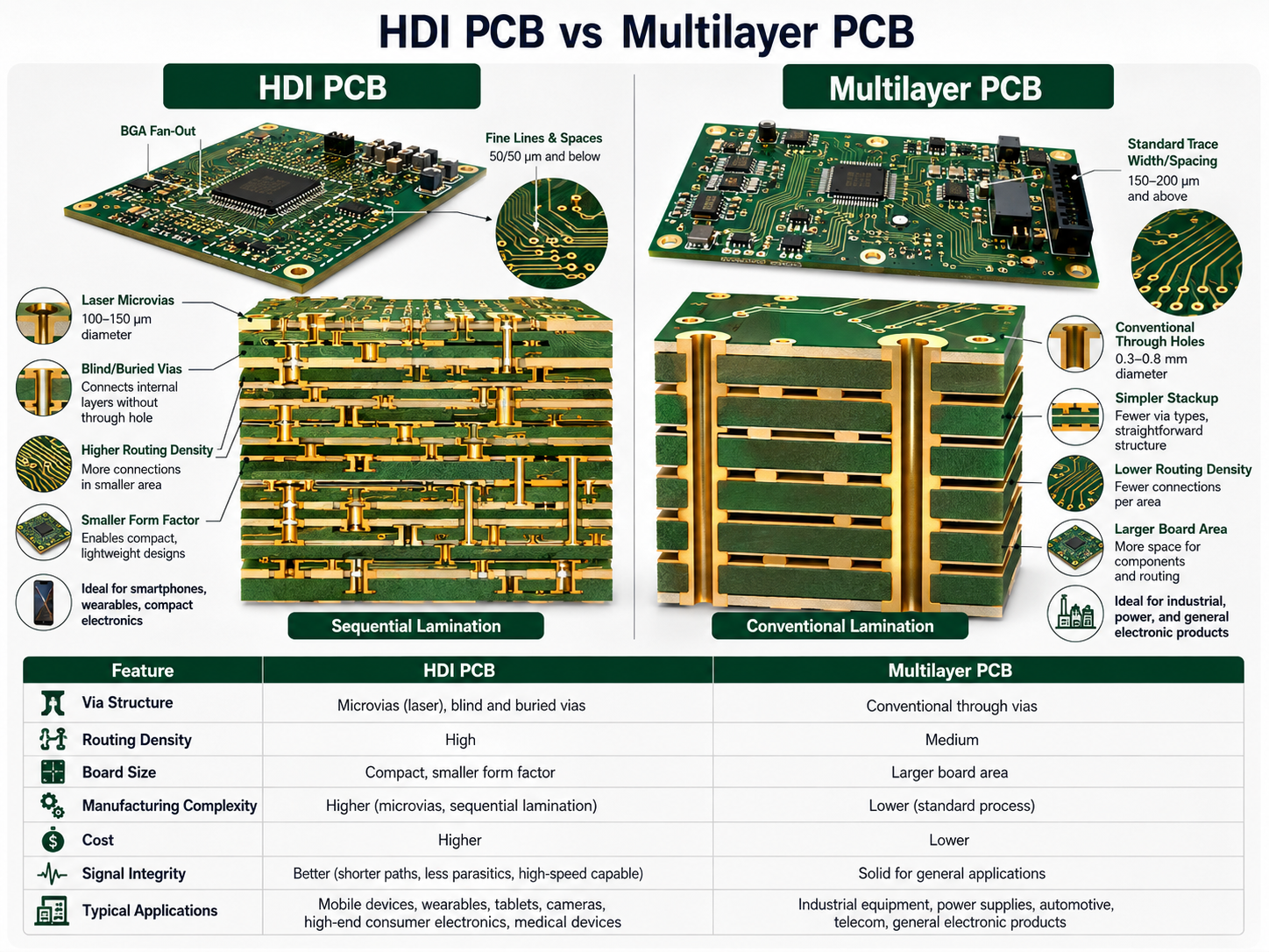
A standard multilayer PCB connects its layers almost entirely with plated through-holes that run through the whole board. An HDI board adds laser-drilled microvias, plus blind and buried vias, so only adjacent layers get linked. That is what lets the same area carry finer traces and far higher routing density.
02
When should I choose HDI over a standard multilayer PCB?
When the board geometry forces you to use BGAs with a pitch down around 0.5 mm or so, trace widths below about 100 microns (less than 4 mils), layers in a high component density scenario that the boards’ planar area or height limitations can’t contain, or for high-speed / RF designs that demand controlled-impedance signal paths that are inherently short and controlled. Barring these exceptions, a standard multilayer board is still likely your least expensive and most efficient route.
03
Is an HDI PCB more expensive than a multilayer PCB?
Per square unit, yes; laser drilling and sequential lamination do increase the cost of bare-board, but HDI can cut the overall layer count and the panel size down, which in some circumstances could translate into a net saving in finished-product costs. So cost wise the general argument would be based on total cost, not bare-board price.
04
Can HDI reduce my layer count and total cost?
Sometimes yes. If your board layout requires 12 traditional layers but microvias give you some available routes, you can often do your layout in fewer HDI layers. Some HDI boards have both fewer layers and smaller footprint so it can be the most cost-effective board — if it reaches a high enough density level. Below that, an HDI board still costs more than a standard one.
05
What BGA pitch requires an HDI design?
As a rule of thumb, components in BGA & CSP packaging on ~0.5mm pitch & under are generally not able to be escape-routed using standard through-hole vias – it doesn’t leave adequate space between the pins. At that point a microvia HDI structure becomes the solution (frequently via-in-pad). Coarser-pitch components seldom require HDI.
06
What are the disadvantages of a multilayer PCB?
Conventional multilayer boards lean on through-holes, which eat routing space on every layer they pass and stretch high-speed signal paths. On very dense or fine-pitch designs they hit a wall — you cannot escape-route the part — and stacking on more layers to compensate adds thickness, weight, and cost.
07
What are the main types of PCB?
By construction: single-sided, double-sided, conventional multilayer, and HDI. HDI is at heart a multilayer board with added microvia (blind/buried) interconnects for higher density — more a construction technique applied to a multilayer stack-up than a wholly separate type.
Interactive Tools
Three Tools to Scope Your Build
03 self-service tools
01
Decision
HDI vs Multilayer PCB Decision
Answer four questions about your design and get an HDI / multilayer / hybrid recommendation with the reasoning.
Open the decision tool
02
Stack-up
HDI Build-Type Selector
Map your density to a starting stack-up — 1+N+1, 2+N+2, or any-layer — with the reasoning behind it.
Open the build-type selector
03
Cost
PCB Cost-Driver Estimator
See which process choices push fabrication cost as a relative complexity index — spot where to simplify.
Open the cost estimatorEngineering Perspective
Our Engineering Perspective
These thresholds — 0.5 mm BGA pitch, sub-100 µm lines, the any-layer-vs-hybrid call — come from how we scope incoming HDI and multilayer work during DFM, not from a datasheet. Where we cite microvia and line-width figures, they reflect industry-standard ranges. Design to whatever your fabricator’s published capability sheet lists, since that is the real limit. We are open about the hybrid build and its benefits because our customers routinely find it saves them money on a first HDI project — even though it is a smaller order for us.
DFM Review
Not sure which build your design needs?
Send in your designs and receive a DFM review with HDI-vs-multilayer call included (with hybrid option when it pays!).