Get in touch with PCBark Company


Updated July 2026 · Reading time ~15 min.
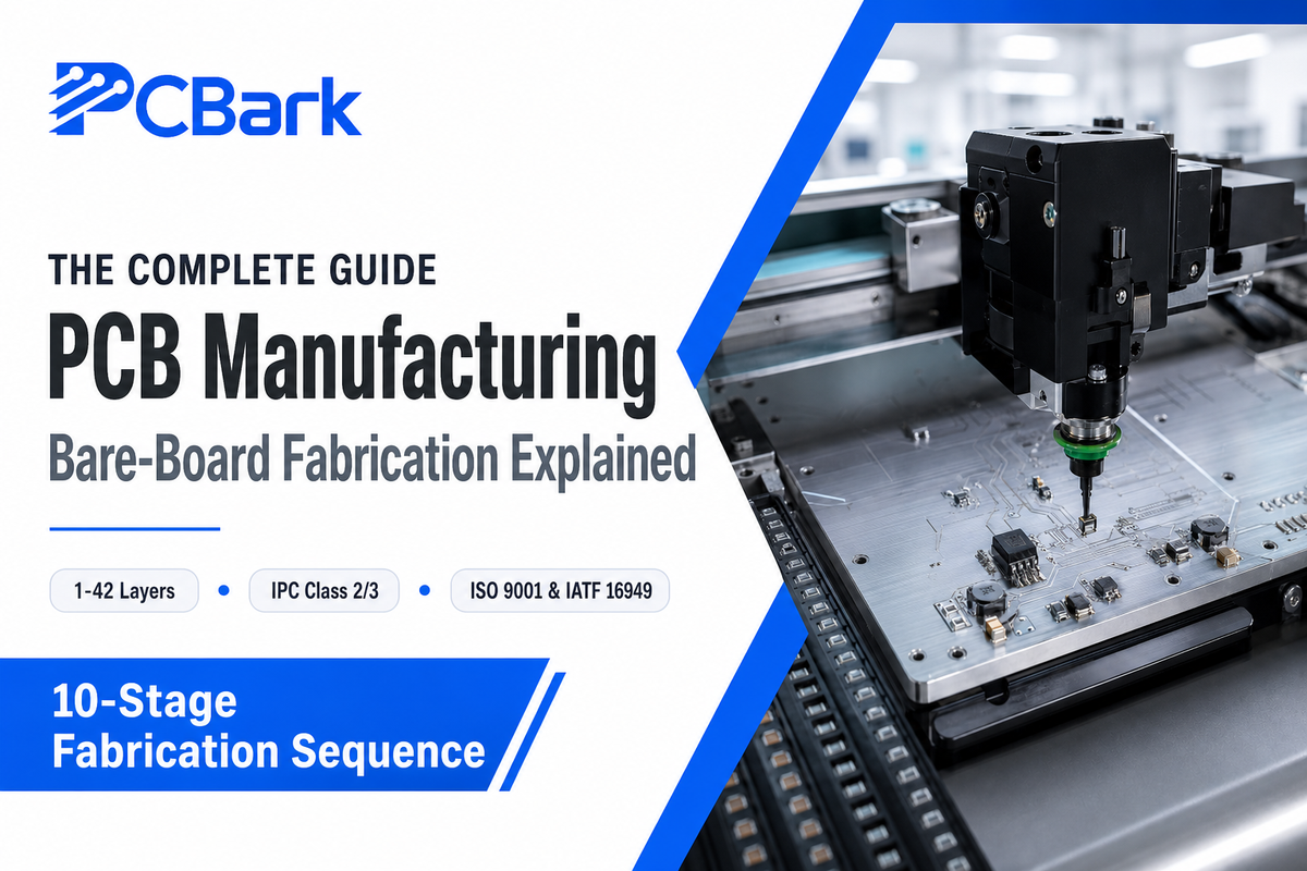
PCB manufacturing is the construction of a bare printed circuit board from copper-clad laminate – etching conductive traces, drilling and plating holes, and applying solder mask and silkscreen – the process that takes place before any component is ever touched by the board. This guide walks through the fabrication process stage by stage, decodes IPC quality classes with real numbers, compares substrate materials, and explains what actually drives landed cost when sourcing from China. If you’re looking for the next step – assembling the bare board with components – see our complete PCB assembly guide.
Quick Specs: PCB Manufacturing at a Glance
| Layer count | 1–42 layers |
| Min trace / space | 3–4 mil (0.076–0.10mm), tier-dependent |
| Board thickness | 0.2mm – 6.0mm |
| Copper weight | 0.5–8 oz |
| Impedance control | ±10% |
| Governing standards | IPC-2221 (design) · IPC-6012F (qualification) · IPC-A-600 (visual) |
What Is PCB Manufacturing?
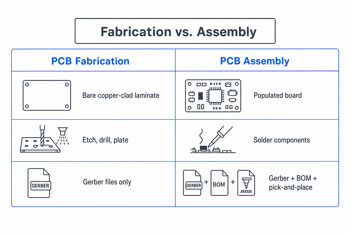
PCB manufacturing, or “PCB fabrication”, is the building of a bare printed circuit board from a copper-clad laminate, including etching the conductive traces, drilling and plating holes, and adding solder mask and silkscreen, all before any components are placed. This line is explicitly stated by IPC in their Production Cycle documentation; their “Printed Board Fabrication” documents refer to standards relating to laminates, surface finishes, plating processes and thermal-stress methodology, while their “Assembly” documents cover materials and components.
It’s incredibly easy to confuse the two stages; ask the question on a PCB forum and you’ll be likely to hear from newer designers wondering about required files for a fabricator, or wondering if a schematic needs to be included with the Gerbers to enable fabrication. A bare board only requires Gerbers for the fabrication manufacturer; once an assembly manufacturer is involved and can attach a Bill of Materials, it’s much easier to reverse engineer a completed design. This makes the unified-roof provider’s life much easier, which is one practical reason why many buyers prefer to source both manufacturing services and assembly services from a single, responsible party rather than splitting pcb assembly services across a second vendor.
The Fab-Assembly Handoff Gap
Often fabrication and assembly are separate processes and can even be separate companies, which adds an extra handoff stage. Every transition creates an opportunity for a fabrication tolerance to misalign with an assembly footprint and an opportunity to have an argument about where responsibility lies when a defect occurs. If one company controls both fabrication and assembly under a unified design and manufacturing quality system, it eliminates that risk of argument; with two separate entities, it simply defers it to later, after the board has failed.
Buyers of printed circuit boards aren’t all created equally either; ranges can be anything from an electronics hobbyist wanting to order a single, low-cost pcb prototype, to a consumer electronics OEM ordering tens of thousands with electronic components pre-sourced against the design, for example. File formats a fabricator can work with, typically Gerber, ODB++ and IPC-2581, matter far more once volume scales up.
| PCB type | Construction | Typical application |
|---|---|---|
| Single-sided | 1 conductive copper layer on one side of the substrate | Low-cost consumer electronics, simple control boards |
| Double-sided | 2 conductive layers, plated through-holes connect them | General consumer and industrial control boards |
| Multilayer rigid | 4-42 layers, laminated under heat and pressure | Servers, telecom infrastructure, complex digital systems |
| HDI (High-Density Interconnect) | Microvias, fine trace/space, Any-Layer stack-ups | Smartphones, AI-accelerator boards, advanced packaging |
| Rigid-flex | Rigid sections and flexible polyimide sections combined in one board | Foldable/compact devices, aerospace and medical assemblies |
| Fully flexible (polyimide) | Fully flexible substrate, one or more copper layers | Wearables, tight non-planar enclosures, battery-pack interconnects |
| Metal-core (MCPCB) | Aluminum or copper base layer for heat spreading | LED lighting, power-converter boards |
| Ceramic (Alumina/AlN) | Ceramic substrate, high thermal conductivity | Power electronics and sensors needing compact heat dissipation |
| Rogers/RF substrate | Low-dielectric-loss laminate | Microwave, millimeter-wave, and RF front-end designs |
What is the difference between PCB manufacturing and PCB assembly?
PCB fabrication builds the physical board; PCB assembly is the subsequent stage where components are populated and soldered onto the board. See our complete PCB assembly guide to learn about the through-hole and SMT processes, IPC-A-610 acceptance standards, and how to choose an assembly vendor.
The PCB Manufacturing Process, Step by Step
Bare-board fabrication is a linear process involving around ten steps between your design data and a fully tested, functional panel – the number rarely changes, but what can go wrong in each step distinguishes a trusted from a problematic fabricator. That handoff process is fairly standardized too, consisting of the industry-standard design package: Gerber (or ODB++) data plus Excellon drill files, a pick-and-place file, part numbers, assembly drawings, and a bill of materials. These are the same files a CAM engineer runs a design-rule check (DRC) against immediately upon receipt, prior to any physical step in the pcb fabrication process. Most fabricators also offer an online gerber viewer, allowing you to visually confirm your board layout prior to submission and check for missed test points or incomplete drill data before it reaches the manufacturing floor.
Some fine-grained processes occur multiple times within the ten stages of bare-board fabrication; excess copper is removed after every cycle using an etch-resist to protect the surviving traces, UV light exposure then cures photoresist in each defined pattern, and CNC milling profiles the finished panel into individual boards as the working board becomes a finished product in the last stage. Changing a stack-up before committing to mass production offers a far more efficient development cycle than attempting the same after, the prototype-to-production bridge holds up best when the recipe never changes between the two.
| Stage | What happens | What can go wrong |
|---|---|---|
| 1. CAM & DFM review | Gerber/BOM/drill files are checked against design rules before any panel is touched. | Missing layers, undersized annular ring, or design-rule conflicts — the top cause of stalled quotes. |
| 2. Inner-layer imaging & etch | Copper-clad laminate is imaged and unwanted copper is chemically etched away, leaving the circuit pattern. | Underetch or overetch shifts trace width outside tolerance. |
| 3. Lamination | Inner layers are pressed together with prepreg under heat and pressure to form the multilayer stack. | Densely packed vias with too little dielectric between them can make lamination physically impossible. |
| 4. Mechanical & laser drilling | CNC drills bore through-holes; UV/CO2 lasers drill microvias for HDI builds. Drilled holes are checked against the design’s aspect-ratio limit before plating. | Drill wander or wrong aspect ratio compromises hole-wall plating reliability. |
| 5. Copper plating | Electroless then electrolytic plating deposits copper on hole walls to make electrical connections between layers. | Thin or voided plating in the barrel — the exact failure Class 3 inspection is built to catch. |
| 6. Outer-layer imaging & etch | Outer copper layers are imaged and etched to final circuit pattern here. | Same underetch/overetch risk as stage 2, now on the visible surface layers. |
| 7. Solder mask & silkscreen | Solder mask protects copper from oxidation and shorts; an inkjet printer applies the silkscreen legend for reference designators and logos. | Misregistration exposes copper that should be masked, or masks a pad that should be exposed. |
| 8. Surface finish | Lead-free HASL, ENIG, OSP, or immersion silver/tin is applied to keep exposed copper solderable until assembly. | Wrong finish for the pitch/shelf-life requirement. |
| 9. Profiling & routing | Individual boards are routed or V-scored out of the production panel. | Panel-fill inefficiency here is a real, avoidable cost driver (see below). |
| 10. Electrical test | Flying probe or bed-of-nails (ICT) verifies net connectivity before the bare board ships. | Skipping this stage is the difference between a bare board and a bare-board gamble (see below). |
List of bare-board fabrication steps (sequence based on CAM/DFM references and IPC production documentation; the precise number varies by fabricator and complexity).
PCB Substrate & Material Types
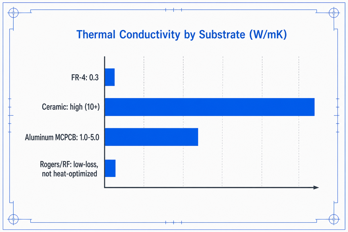
The substrate choice for a board is ultimately an electrical and thermal consideration before it’s a cost decision. An LED driver on standard FR-4 substrate will likely overheat and fail prematurely, while an RF front-end on the wrong material will experience undesirable frequency drifts. Six major families of substrates cover most board design needs, each tailored to solve specific problems. NASA’s own procurement quality-assurance standard for printed circuit boards treats this kind of material specification as a first-order acceptance criterion, not an afterthought, for exactly this reason.
The Six-Substrate Fit Test
- FR-4 — general purpose cost baseline, suitable for most control, IoT and consumer boards with typical thermal and RF performance needs.
- Aluminum/Metal-Core PCB (MCPCB) — the best value solution when heat removal is the primary constraint, thanks to thermal conductivity of 1.0-5.0 W/mK against FR-4’s own roughly 0.3 W/mK (through-plane) baseline — several times higher, and up to an order of magnitude at the top of the range. Primarily used for LED lighting and power electronics applications.
- Ceramic (Alumina/AlN) — the selection of choice when excellent thermal conductivity and RF performance are needed in a compact size for power electronics or sensors. Real world cost can be significantly higher than other substrate types.
- Rogers/RF Substrate — best when low dielectric loss at microwave and millimeter-wave frequencies is critical, carrying significant cost compared to FR-4 or Aluminum.
- Heavy Copper (to 8 oz) — the material for when a high current carrying capacity is needed. It’s often found in power distribution boards and vehicle electronic designs. Keep in mind design rules will likely widen as copper weight increases (more on this under Fabrication Capability & Design Rules, next).
- Polyimide Flex/Rigid-Flex — the choice for when a flexible and/or bendable PCB is required. Ideal for tight, non-planar enclosures or where the board needs to flex during assembly.
Most modern substrate and finish options assume default operation on RoHS-compliant, lead-free processing. Thin copper foils route more readily across different layers of dense HDI stacks, another manufacturability issue worth addressing with your PCB designers before your stack-up becomes fixed.
Nor is the demand side of that list static. The flexible/polyimide-flex PCB submarket alone is anticipated to grow from approximately $28.4B (2025) to $31.1B (2026) at a CAGR of 9.5%, a substantially faster rate than the printed circuit board fabrication market overall, largely because of the increased adoption of electric vehicles, where flex circuits suit the compact and irregular regions within battery packs and motor controllers that rigid boards can’t reach.
Fabrication Capability & Design Rules
These design considerations, minimum trace width and annular ring, more than anything, are what the designers of printed circuit boards test against the limits specified by a fabricator prior to finalising their designs, which are governed by IPC-2221 – the Generic Standard on Printed Board Design – an independent document from the qualification and performance specifications covered next under Quality Standards, and the distinction is significant as they’re commonly confused. At PCBark, the base setting in their DFM assessment for the minimum trace width/space is 4 mil (0.10mm), reducing to 3 mil (0.076mm) for more complex builds such as HDI tier components, a layered pattern used by most fabricators, though very few display it on their website.
| Parameter | Typical range | Why it matters |
|---|---|---|
| Layer count | 1–42 layers | Higher layer counts unlock HDI backplanes and RF stacks; most fabricators cap well below 42. |
| Min trace/space | 3–4 mil (0.076–0.10mm), tighter on request | Fine-pitch BGA escape routing needs the tighter end of this range. |
| Min annular ring | 0.05mm (2 mil), IPC-6012 Class 2 baseline | Undersized annular ring is one of the most common DFM rejections (see below). |
| Copper weight | 0.5–8 oz | Heavier copper needs proportionally wider trace/space and larger minimum holes. |
| Impedance control | ±10%, tighter per stack-up | Set at quote time from your stack-up, not a fixed universal number. |
📐 Engineering Note
More than 30% of the Gerber data packs one established PCB sourcing group receives contain design errors, ambiguous information, or conflicts between the data and the stated specification. One documented case: a 10-layer board with 0.075mm microvias and blind/buried via pairs hit a six-week delay because the chosen fabrication manufacturer could not hold the tolerance — redesigning with standard stacked vias and 0.1mm drill sizes cut the cost by an estimated 15% for this illustrative case and resumed production inside ten days. Confirming a fabricator’s real capability index before committing to a stack-up is the actual lesson here — not “avoid microvias.”
“We check every incoming design against this same capability index before we quote, layer count, aspect ratio, copper weight, and impedance. If a board sits at the edge of our window, the buyer hears it during DFM, not after the panels are etched.”
PCBark CAM Engineering Team
Although it’s a prevalent misconception, a board doesn’t become more complex or expensive by having more layers. An examination carried out by a registered PCB design engineer discovered that some manufacturers in China provide comparable prices for 2-layer and 4-layer PCBs, and an extension in the manufacturing time frame could potentially lead to a reduction in cost for a 4-layer board relative to a similar 2-layer board. Paradoxically, due to the use of dedicated plane layers for power and ground to avoid interference with signal routing, routing a 4-layer board is typically easier than a 2-layer board.
Quality Standards Decoded: IPC Class 2 vs Class 3
Selecting the highest IPC class doesn’t necessarily mean choosing the safer option. In most scenarios, the cost-effective choice of Class 2 can provide a comparable level of functional reliability; the prevailing industry consensus is that manufacturing to Class 3 without an exceptional reason (e.g., a mission-critical system or a harsh environment application) is “unnecessary and over-engineered.”
| Criterion | Class 2 (dedicated service) | Class 3 (high reliability) |
|---|---|---|
| Internal annular ring | Relaxed (breakout allowed) | ≥ 1 mil, near-perfect registration required |
| External annular ring | Relaxed | ≥ 2 mil |
| Plated-hole voids | 1 void allowed per 20 holes (5%) | No voids permitted |
| Copper plating thickness | 0.8 mil nominal | 1.0 mil / 25µm minimum |
| Copper thickness tolerance | 0.8–1.2 oz/ft² on 1oz nominal (~28–42µm) | 0.9–1.1 oz/ft² (~31.5–38.5µm) |
The choice of IPC class is final and immutable throughout the production process and can’t be altered after the board is manufactured. It isn’t possible to manufacture a Class 3 end product using a bare Class 2 PCB, so the chosen class must be specified in your purchase order at the initial stage.
Is PCB manufacturing hard?
For a simple 2-layer FR-4 board to Class 2, this is commodity work that just about anyone competent can do. It rapidly becomes much more complicated when you pile on multiple, potentially conflicting requirements like microvias, heavy copper, and precise impedance control, combined with Class 3 workmanship – these need real process controls beyond shop-floor equipment. Difficulty is a function of how many constraints stack on one board, not of PCB fabrication itself.
Inspection & Testing: How Bare-Board Defects Are Caught
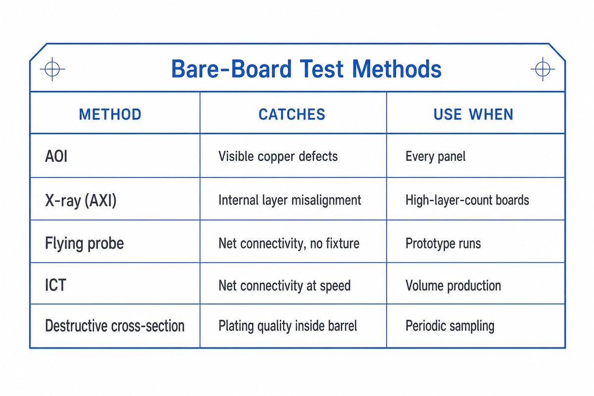
The problem is that no single bare-board test method catches everything; a complex, high-layer-count board needs more than a quick visual inspection, and the quality of a fabricator’s test stack should correlate to the complexity and class of the board being built.
| Method | Catches | Use when |
|---|---|---|
| AOI (automated optical inspection) | Visible copper defects, registration, missing features | Every panel, every layer |
| X-ray (AXI) | Internal layer misalignment, buried defects invisible to AOI | High-layer-count and blind/buried-via boards |
| Flying probe | Net connectivity (opens/shorts), no fixture required | Prototype and low-volume runs |
| ICT (bed-of-nails) | Net connectivity at speed, fixture cost amortizes at volume | Higher-volume production runs |
| Destructive cross-section | Actual plating quality and thickness inside the hole barrel | Periodic process-qualification sampling, not every board |
Beyond what’s on the above table, a functional test stack should also include an impedance coupon, etched on the edge of every board panel so that actual impedance can be compared to the intended value, and periodic samples, or small areas of a board, sectioned out for direct examination after plating. Plating inside a via is subject to various process steps that, if flawed, cause a void in the via wall, a defect that might pass visual inspection and only cause problems months later, after a board has undergone several cycles of heating and cooling. IPC’s own automated-inspection process standards exist precisely to catch this class of latent, delayed-onset defect before it reaches the field.
Certifications & Compliance: What to Verify Before You Order
It’s important to know that the logos on the fabricator’s website only attest to the fact that they were certified at one time – certificate registration numbers expire and have to be renewed after a certain period, and are only valid until their next inspection.
High-quality PCB fabrication is more than a matter of just holding certificates such as ISO 9001 and IATF 16949.
⚠️ Important
Two layers of compliance are almost never listed on the buyer checklist. In the U.S., printed-circuit board manufacturing falls under EPA 40 CFR Part 413 Subpart H — pretreatment of wastewater discharge limits — which places restrictions on metals such as cyanide, copper, nickel, chromium, zinc, lead, and cadmium for any discharge that goes to a public treatment system.
Also relevant: UL 796 (Safety for Printed-Wiring Boards) is a separate end-product safety standard from the UL 94V-0 flammability classification alone; UL 796 covers construction and performance of the final board, not just the raw materials used.
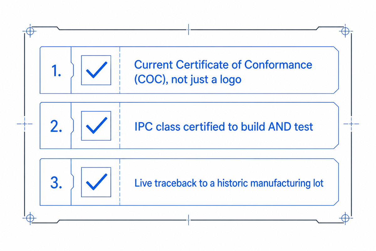
The due diligence here boils down to a very short list: ask for (1) a current copy of the fabricator’s Certificate of Conformance (COC) in PDF format (not just the logo); (2) which IPC class they’re certified to build and test to, along with the qualification levels of their test operators; and (3) request a live traceback to a historic manufacturing lot. Failure to produce one of these indicates something important.
Likewise, sourcing integrity should be considered. This includes having all components and materials stocked in-house and having a policy that requires customer approval before making substitutions to prevent any covert component swapping, an issue NIST considers separate from workmanship class.
China-Cost Sourcing: What Actually Drives Landed Cost
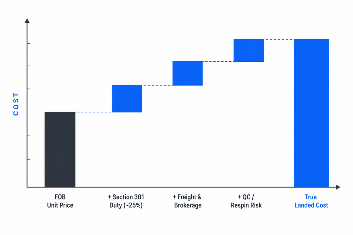
A quoted unit price isn’t a landed cost, and where the two become equated, the “cheap board” regret generally starts – regardless of whether you’re ordering a one-off prototype pcb from a quick-turn pcb fabricator or a 5,000-unit production run. Today, most fabricators offer some sort of instant quote tool for simple board designs, but an automated quote is only as reliable as the underlying file package it consumes.
The Landed-Cost Reality Check
Consider a 4-layer rigid board quoted at $2.00/unit FOB China for a 5,000-unit run – a $10,000 line item. If you then apply the verified 25% Section 301 duty on HTS 8534 (bare printed circuit boards), the duty alone will run $2,500 – not including freight, customs brokerage or the cost of an escape to quality control. That alone represents a premium of about 25% over the FOB unit price. Moreover, further layered tariffs introduced last year may drive this figure even higher on some types of boards (HDI, flex and multilayer PCBs carry different tariff classifications than simple 2-4 layer rigid boards), so check with your customs broker to determine the precise rate on your particular HTS sub-classification rather than assuming a flat 25%.
And duty isn’t the only non-quoted item that can sink a “cheap” board — an industry-cited $28,500 average, with respins averaging about 2.9 board iterations at 16 days per iteration, could easily dwarf the entire duty payment on a medium-sized run, for example. Quoted price versus actual cost is where sourcing decisions actually get made, and regretted.
The idea that offshore sourcing is inherently less costly is another common, related presumption that warrants careful examination. After taking all costs into account – extra inventory for the longer lead times offshore, resourcing cost for when a board is close to but not within specification, the risks of counterfeit component supply in unmanaged overseas supply chains – what initially looks like savings per unit could be offset, or even reversed, by the costs. It doesn’t mean offshore sourcing is the wrong approach – it simply means that landed cost, not quoted unit price, must be the driving input into any sourcing decision.
The 2026 Outlook: What’s Actually Changing in PCB Manufacturing
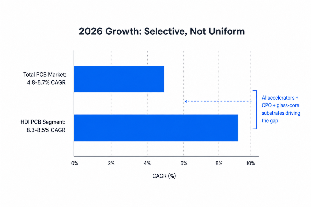
The market for PCBs isn’t just growing; it’s growing at a selectively uneven pace – and that’s where the 2026 story lies, not in overall market sizing. Demand for HDI PCB is growing at an estimated 8.3-8.5% CAGR versus the total PCB market’s growth rate of 4.8-5.7% (both figures approximate, as they vary across research reports), a speed gap that suggests specific segments of demand are pulling growth in the direction of high-value, high-density products, not uniformly raising all boats.
There’s a name for that pull: hyperscale data-center operators purchased 3.5 million-plus AI accelerators in 2025, a year-over-year increase Mordor Intelligence puts at roughly 180%, and every single new GPU card requires 32-layer boards with impedance-controlled differential pairs below 10µm line/space. Co-packaged optics (CPO) hit volume shipment in 2025, squeezing switch motherboard area by around 30% while requiring IC substrates with via densities greater than 10,000 per cm² – that’s a technology shift, not a forecast. Even more forward looking is a transition underway towards glass-core substrates: an independent SEMI/Global Net Corp industry report (May 2026) projects initial production around 2028 and a 67.2% CAGR from 2028 to 2040 as artificial intelligence and high-performance computing drive demand for larger, more advanced packages, with an October 2025 Ibiden-Corning partnership among the concrete steps already underway. This signals the next major material shift, beyond the limitations of today’s organic substrates.
The standards are adapting to meet these needs. Global Electronics Association (formerly IPC) standards also evolved to meet the challenges with a raft of 2026 standards specific to this trend — IPC-6921 for organic IC substrates and IPC-9711/9712/9716A for automated inspection processes, including 9712, which was developed specifically for IC substrates. Separately, there’s a move to get liquid-cooled AI server boards into IPC-6012 Class 3L qualification, a status only achievable by a subset of the most established Tier-1 manufacturers, due to two-to-three-week lead time additions associated with the conformal coating and underfill steps required for liquid immersion. Adding a second independent pull to the same HDI/multilayer segment, EV and 5G infrastructure rely on high-density, high-reliability board types, including for their base stations, EV control units and ADAS sensor assemblies — a fact that points to a fundamental, industry-wide demand shift, not a one-time event.
In addition to riding the demand side, automation is beginning to make inroads into the fabrication process itself. Layout-automation tools are shortening the design cycle at the front end, and on the shop floor, automated quality tracking and AI-powered inspections are reducing the number of false alarms without sacrificing quick turnaround in the quick-turn space — that’s the 2026 production side.
Frequently Asked Questions
Q: What is PCB manufacturing?
PCB manufacturing is the fabrication of a bare printed circuit board from copper-clad laminate, using etching, drilling, and plating, all before any components are mounted onto the finished panel.
At a high level, PCB fabrication involves imaging and etching the copper trace, drilling and plating the vias, and applying solder mask and silkscreen, or in approximately 10 stages, a design file becomes a completed, tested panel. This is typically followed by component mounting in a distinct process called PCB assembly (PCBA), which is often handled on a separate line and sometimes by a separate entity, so clients seeking a single point of accountability may prioritize a fabricator that offers assembly as part of their services.
Q: Is PCB manufacturing hard?
Routine work covers a simple 2-layer FR-4 board built to Class 2; difficulty rises fast once you stack HDI, heavy copper, tight impedance, and Class 3 acceptance together.
Difficulty arises as the number of challenging design parameters on a given board increases-the challenge scales with the difficulty of that design, rather than being a general challenge to the PCB fabrication industry as a whole. Checking that supplier’s published capability index table (see above) is the simplest way to tell whether a given combination is routine for them or a stretch.
Q: Who is the largest PCB manufacturer in the world?
Rankings shift by revenue methodology, whether assembly revenue is counted alongside fabrication, and change year to year; treat any single “largest manufacturer” claim as a snapshot, not a fixed fact.
Most global PCB manufacturing is performed by a few very large Asian players, but when you look at published rankings of “biggest” companies it really depends on whether you are counting only fab revenue, or fab and assembly, the currency of reporting, and the year. A company listed as #1 this quarter can be #3 next quarter due to minor changes in how the revenue is counted or in the exchange rate of a few currencies. But this kind of noise in rankings really doesn’t matter that much for sourcing: the real key is whether a fabricator has a real DFM process, good DFM discipline, certs that are actually verified and, most importantly, a solid published capability index. You won’t find these on “who’s #1” lists.
Q: What files do I need for a PCB manufacturing quote?
Gerber (or ODB++) files, a drill file, and your layer count, thickness, and finish requirements are the minimum; a stack-up drawing speeds the DFM review.
Bare PCB fabrication (as opposed to a full assembly) doesn’t require a BOM or a centroid file — these come in play with the components. If you don’t have a stack-up drawing, a fabricator that truly offers DFM reviews should work with you to create one instead of just giving you a guess.
Q: How long does PCB manufacturing take?
Bare-board lead time depends heavily on layer count, build class, and current factory queue; always confirm a quoted lead time against your specific stack-up rather than a generic website promise.
High-layer count boards and Class 3 boards require more processes and inspection and will naturally have longer lead times than standard 2-4 layer boards. Always ask what’s included in the quoted lead time. A number that doesn’t consider your queue position and build complexity isn’t much of a lead time at all.
Q: What’s the difference between PCB manufacturing and PCB assembly?
Manufacturing (fabrication) builds the bare board; assembly mounts and solders components onto it afterward — two different production lines, sometimes handled by two entirely different companies.
When sourcing a turnkey provider (where a single entity does both fab and assembly), understand how a shared quality system bridges any gap between fab tolerances and assembly footprints before you sign. See our complete PCB assembly guide to learn about the PCBA process itself, IPC-A-610 acceptance criteria, and the trade-offs between turnkey and consigned sourcing models.
Q: Is “PCB” the same as the banned chemical?
No, not at all. In electronics, PCB means printed circuit board; the banned chemical sharing the same three-letter acronym is polychlorinated biphenyl, an entirely unrelated industrial compound.
Two words with distinct meanings but that often show up together in searches.
Related Reading
- PCB Assembly: The Complete PCBA Process Guide – covers pcb assembly services in depth, the stage following PCB fabrication.
- Our full PCB manufacturing capability page – Detailed information on our PCB fabrication capacity and processes.
- Our DFM review process – A description of our 8-point DFM inspection procedure for incoming designs.
- AOI, X-ray, and flying-probe inspection capabilities.
- Our certifications page – Details about our certifications including ISO 9001, IATF 16949 and workmanship standards.
- Multilayer PCB capabilities
- HDI PCB capabilities – Information related to our advanced HDI capabilities relevant to the projected 2026 market trends.
- Aluminum / metal-core PCB
- Rogers PCB / RF substrate
- Heavy copper PCB
- Turnkey PCB assembly
- Medical PCB requirements
About This Guide
This guide is informed by the latest available data and references: IPC-2221, IPC-6012F, IPC-A-600, and IPC-A-610J published by IPC (the Global Electronics Association), a NASA standard for PCB procurement, U.S. Environmental Protection Agency (EPA) pre-treatment standards, current guidance from the United States Trade Representative (USTR) under Section 301 of the Trade Act of 1974 regarding tariffs on imports from China, and industry-reviewed research on Design for Manufacturing (DFM) practices and market trends. Where possible, estimates have been provided to reflect typical variations for given parameters. Any figures provided are intended as guidelines and specific details may vary depending on the nature of the board. Provided by the Shenzhen Linghangda Technology (PCBark) engineering team.
The Team Behind This Report
PCBark fabricates printed circuit boards from 1 to 42 layers across six substrate families in an ISO 9001 and IATF 16949 certified factory. Capability numbers, the IPC class table, and landed-cost math in this guide are the same reference points our own CAM engineers check every incoming Gerber file against before quoting, publishing them here is the same discipline we apply on the shop floor, not a separate marketing exercise.