Get in touch with PCBark Company

PCBark · Electronic Manufacturing Services · IPC-A-610 / J-STD-001
PCB Inspection: AOI, X-Ray, Flying Probe & ICT
PCBark closes that gap by combining 4 inspection techniques for complete board-level coverage. It’s our guarantee that the board you approve is the board that ships – 100% visible, 100% under, 100% conductive.
That Gap is Expensive
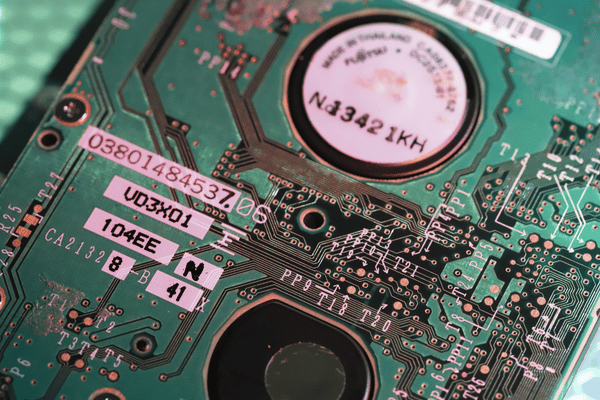
Field returns rarely trace to a defect you can see – a voided BGA joint, an open via, a hairline short under a connector. PCBark runs four inspection methods against every pcb assembly so the board you approve is the board that ships. AOI checks every visible joint, X-ray sees under the BGAs, and flying probe or ICT confirms the board is electrically sound.
Inspection Coverage
Methods
4 Methods
AOI · X-Ray · Flying Probe · ICT
AOI Coverage
100%
AOI coverage of placed components
Hidden Joints
BGA / QFN
Hidden solder joints via X-ray
X-Ray Imaging
2D / 3D
X-ray imaging incl. CT & laminography
Acceptance
IPC-A-610
Acceptance class 2 & 3
Experience
16+ yrs
EMS inspection experience
01 / The Problem
Catching the Defects You Can’t See
pcb inspection is the set of optical, X-ray and electrical checks that verify a printed circuit board is built and connected the way the design intended. The problem is that no single method catches everything. automated optical inspection reads the top of the board well, but it cannot look under a ball grid array. An electrical test proves the net is connected, but it will not flag a solder joint that is 40% voided and will crack after a year of thermal cycling. inspect with one method and you ship the gap between them.
Reads the top of the board well, but it cannot look under a ball grid array.
Proves the net is connected, but will not flag a solder joint that is 40% voided.
02 / The Cost & The Fix
That Gap Is Expensive — So We Layer Four Methods
That gap is expensive. A missing component, an insufficient-solder joint, a misaligned part or a void hidden in a BGA ball usually survives a quick visual check and fails in the field, where the cost to fix it is an order of magnitude higher than catching it on the line. PCBark closes the gap by layering four inspection methods so optical, radiographic and electrical coverage overlap — each method catches the defects the others are blind to. The rest of this page breaks down what each method detects, how they compare on real terms, and how we match an inspection plan to your board and volume.
Already know the defect you’re chasing? Tell us your board type and we’ll scope the inspection coverage.
Scope My Inspection Coverage →01 / Inspection Stack
PCBark’s 4-Layer Inspection Stack — AOI, X-Ray, Flying Probe & ICT
Each method below targets a different physics of failure. optical inspection sees what light can reach; x-ray inspection sees through solder and metal; electrical test confirms the circuit actually conducts. On most assemblies we combine two or three of them – AOI plus X-ray for the visible and hidden solder, plus flying probe or ICT for the electrical net. Each card explains what it detects and where it fits.
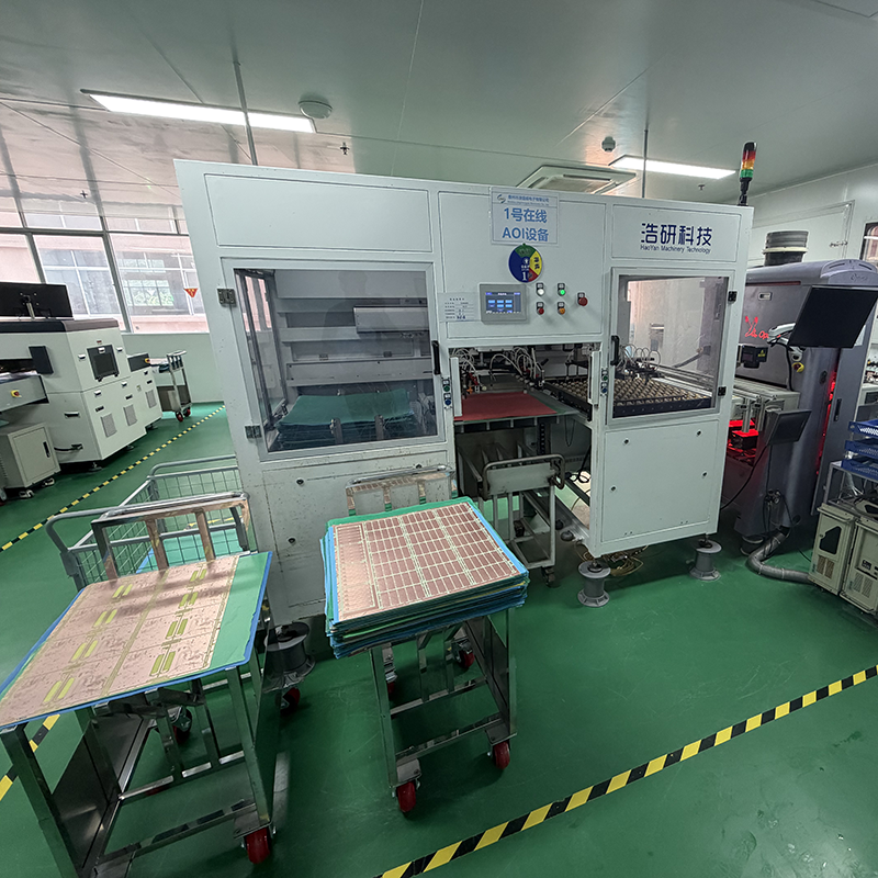
Automated Optical Inspection (AOI)
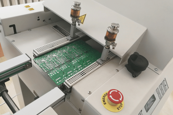
A non-contact optical inspection method. High-resolution cameras image every placed component and compare it against a known-good reference to identify defects across 100% of the board.
Read moreShow less
Detects: missing components, misaligned / tombstoned parts, wrong polarity, solder bridges, insufficient solder, lifted leads, surface scratches
- Runs inline after reflow – fast enough for any volume
- No fixture; the cost is one-time program setup per PCB assembly
- Blind spot: cannot see under BGAs, QFNs or shielding
Best for: every board, as the first-pass screen
X-Ray Inspection (AXI)
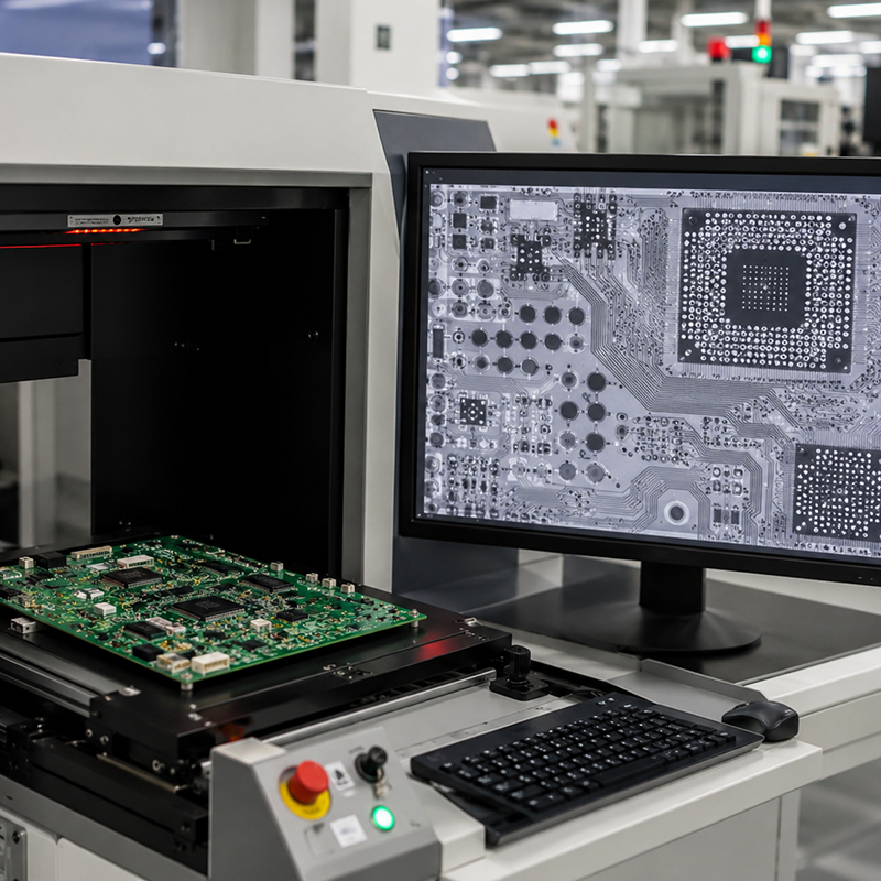
Automated x-ray inspection looks through the assembly to image hidden solder joints – the ones under ball grid arrays, QFNs and bottom-terminated parts on dense boards like any-layer HDI that AOI and the naked eye never reach.
Read moreShow less
Detects: BGA voids, head-in-pillow, open / bridged hidden joints, insufficient solder, component misalignment, internal shorts
- 2D for fast screening; 3D, computed tomography (CT) and laminography for cross-section views at different angles
- Non-destructive — the same board moves on to assembly; modern X-ray inspection systems pair a microfocus tube with a flat-panel detector
- Essential on high-density and BGA-heavy boards in PCB manufacturing
Best for: BGA / QFN, high-reliability, high-density boards
Flying Probe Testing
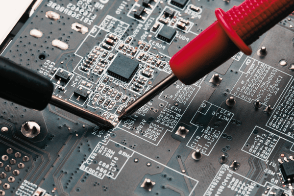
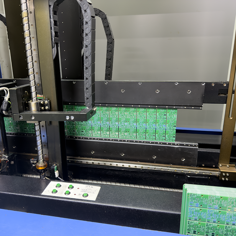
A fixtureless in-circuit test. Movable test probes “fly” across the board to contact test points and measure resistance, capacitance and continuity – no custom test fixture, so a new design can be tested in days, not weeks. Because the flying probe tester runs from a test program, it is a fast testing solution for new revisions — test coverage is defined in software and test time scales with the net count, not a fixture build.
Read moreShow less
Detects: opens, shorts, wrong / missing component values, diode orientation
- No bed-of-nails fixture – only a test program, generated from the netlist
- Probes both sides of the PCB; ideal when test points are limited
- Slower per board than ICT – suitable for prototypes and low-to-mid volume
Best for: prototypes, NPI, low-volume, design changes
In-Circuit Testing (ICT)
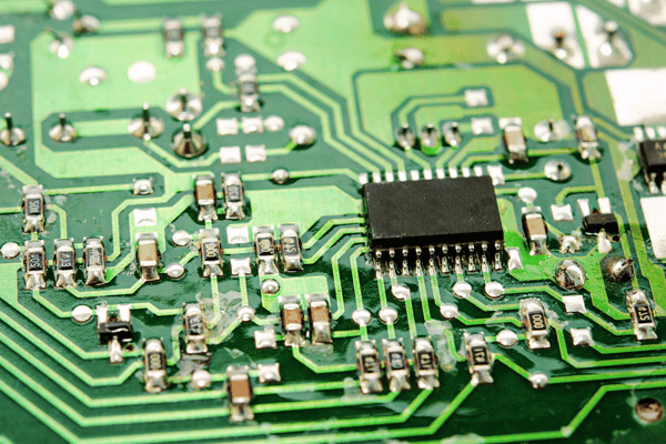
A bed-of-nails fixture presses spring pins onto dedicated test points to test components and connections in parallel. Its fixture costs more up front, but once built it tests a board in seconds.
Read moreShow less
Detects: opens, shorts, component value / presence faults at high coverage
- Custom test fixture required – a one-time NRE cost per design
- Very fast per board once the fixture exists
- Needs accessible test points designed into the PCB layout
Best for: stable, high-volume production
02 / Engineering Note
BGA Void Acceptance
X-ray inspection earns its place mainly on the BGA. Because the solder balls sit under the package, the only point in the manufacturing process where you can confirm wetting and measure voiding is radiographically. Many programs apply the voiding guidance in IPC-7095 and the acceptance criteria in IPC-A-610 – a frequently used production limit is roughly 25% void area per ball, tightened for Class 3 hardware. The right threshold depends on your acceptance class and the part, which is something we set with you before the first build rather than after a reject.
Knowing what each method costs to run and how fast it clears a board is what actually drives the inspection plan.
01 / Method Comparison
AOI vs X-Ray vs Flying Probe vs ICT — Method Comparison
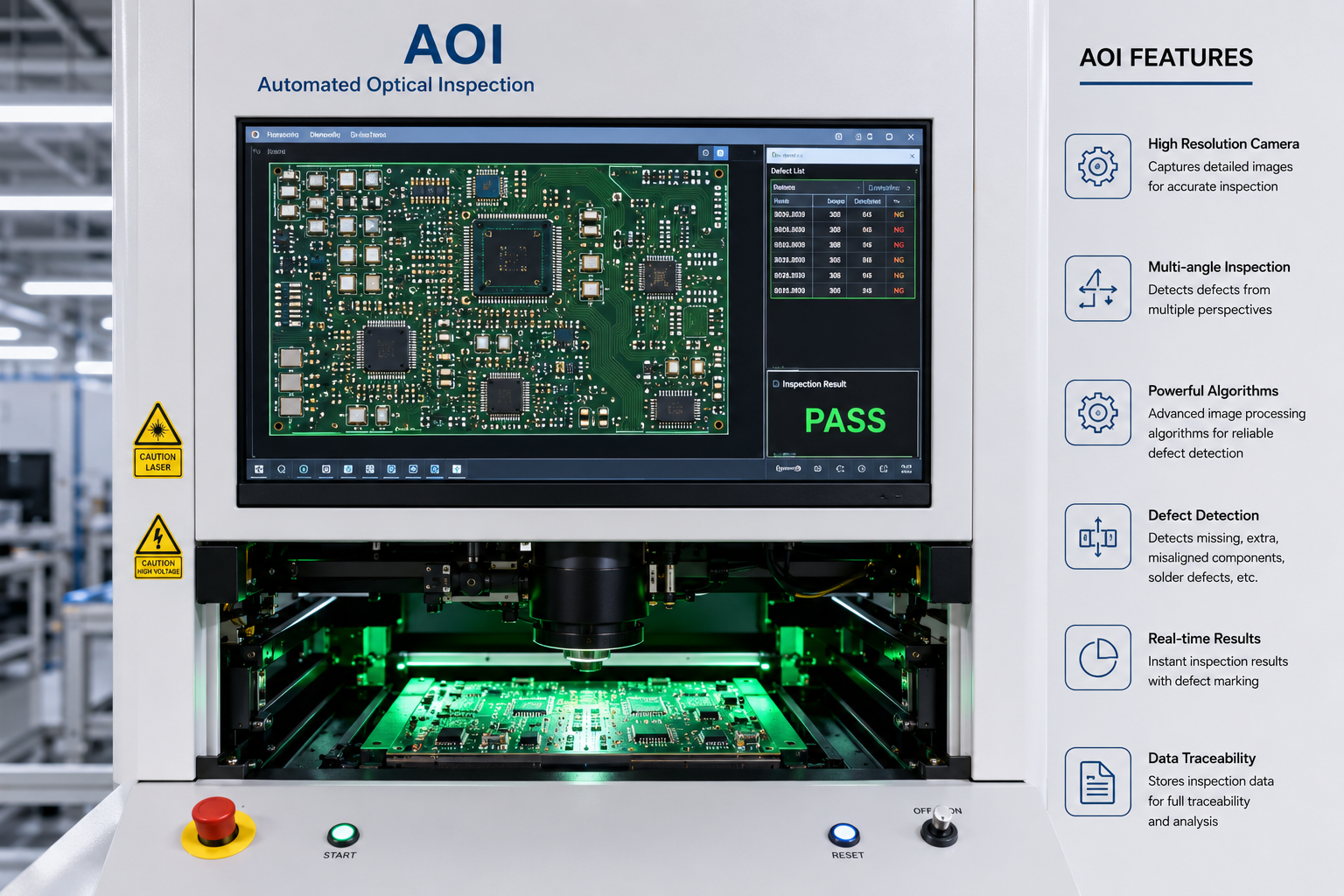
No method is “best” in isolation – they trade coverage, speed and setup cost against each other. AOI and X-ray are inspection (they look at the joint); flying probe and ICT are test (they prove the circuit conducts). Our comparison below weighs them on the terms that decide an inspection plan: what they detect, how they scale with volume, and where the cost sits.
| Method | What it checks | Hidden joints | Volume fit | Fixture | Main cost driver |
|---|---|---|---|---|---|
| AOI | Surface & placement defects, visible solder | No | All volumes | None | Program setup (one-time) |
| X-Ray (AXI) | Hidden BGA/QFN joints, voids, internal shorts | Yes | All; key for BGA | None | Scan time per board |
| Flying Probe | Opens, shorts, R/C values electrically | Electrical only | Proto & low-mid | None | Test-program development |
| ICT | Opens, shorts, component value at high coverage | Electrical only | High volume | Bed-of-nails | Fixture NRE (one-time) |
02 / Budgeting Pattern
The Crossover Is Volume
One pattern matters for budgeting here: flying probe and ICT reach the same kind of electrical faults, but the crossover is volume. Flying probe carries no fixture cost and starts testing almost immediately, so it wins for prototypes and low volume; ICT carries a fixture cost but tests in seconds, so it wins once volume is high enough to amortize the fixture. AOI and X-ray are not interchangeable with either – they catch solder and placement defects that an electrical test passes straight over, which is why a sound plan pairs an optical/X-ray layer with an electrical layer rather than choosing between them on real PCB assemblies.
01 / Quality Results
Inspection Built Into Assembly — Quality Results & Applications
At PCBark, inspection is not a service you buy separately – it is how a high-quality board gets built, layered straight into our circuit card assembly line. Boards move from solder paste inspection through AOI, then X-ray for the hidden joints, then flying probe or ICT for the electrical net, before final visual inspection. Because the checks are layered, a defect that slips past one stage is caught at the next, which is the whole point of a multi-method inspection process: drive the defect escape rate toward zero before the board leaves the building, and feed every reject back into quality control.
Industry “rule of ten”: the cost to find and fix a PCB defect rises roughly an order of magnitude at each stage it escapes — bare board, to assembly, to field. Inspection moves the catch upstream, where it is cheapest.
QUALIFIED Cost-of-quality “rule of ten” is a widely cited industry heuristic; actual ratios vary by product and program.
02 / Applications
Where the Method Mix Changes
This becomes more important in areas where field failure is less a warranty item and more a safety and mission critical event. Here are the changing method mix for those applications:
Automotive
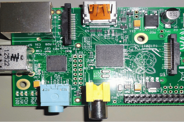
High-reliability electronics under vibration and thermal cycling — AOI plus X-ray on every BGA, with electrical test for connectivity.

Aerospace & Defense
Class 3 acceptance, 100% X-ray on critical joints, and documented inspection records for the supplier-qualification file.
Medical Devices
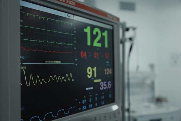
Traceable inspection to IPC-A-610 Class 3, with functional verification on assemblies where a fault has patient impact.
Industrial & IoT
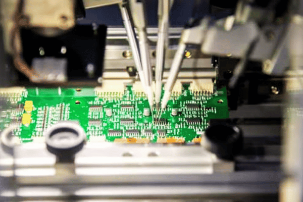
Cost-balanced AOI + flying probe for prototypes and ramp, moving to ICT as volume stabilizes.
Those reliability levels are only real if they can be tied to a known standard.
01 / Standards & Compliance
Standards & Compliance
All PCBark inspection decisions trace to an published acceptance standard – never just an in-house opinion. That enables both a quality engineer to repeat our pass/fail call and a buyer to drop our inspection records into their own supplier qualification file.
IPC-A-610
Acceptability of electronic assemblies · Class 2 & 3
J-STD-001
Soldered electrical & electronic assemblies
IPC-A-600
Acceptability of printed boards
IPC-7095
BGA design & assembly / void criteria
ISO 9001
Quality management system
Procurement Note
For that reason ask your inspection supplier what acceptance class and Revision they use before comparing quotes. “We do x-ray” versus “we x-ray to IPC-A-610 Class 3 with documented void limits” are vastly different buys. We encourage you to document the specific certificate numbers and revision levels that will be used on your quote for your supplier qualification file.
01 / Inspection Quote
Getting a PCB Inspection Quote — Coverage, Turnaround & What’s Included
That’s why not all inspection quotes are equal. It is easy to quote “PCB test services” with two very different meanings — one being little more than a quick AOI pass, the other being AOI, full X-ray on BGAs, and electrical test.
Inspection Plan by Board Profile
| Board profile | Typical volume | Recommended inspection mix | Why |
|---|---|---|---|
| Prototype / NPI | 1–50 | AOI + Flying Probe + X-ray (BGA) | No fixture cost; fast turn on design changes |
| Low volume | 50–1,000 | AOI + Flying Probe + X-ray (spot) | Electrical coverage without ICT tooling |
| Mid volume | 1,000–10,000 | AOI + X-ray + ICT (if test points designed) | Fixture starts to pay back |
| High volume | 10,000+ | AOI + ICT + X-ray (AXI sampling) | Seconds-per-board electrical test |
| BGA-dense / high-reliability | any | AOI + 100% X-ray + Functional test | Hidden-joint and field-failure risk |
02 / What’s Included
What’s Included in Your Quote
What is included in your PCBark inspection quote: the method mix above, the acceptance class and void criteria we will inspect to, and the inspection report we ship with the boards. Because inspection is part of our turnkey EMS process — DFM review, component sourcing, fabrication, SMT assembly, then test — the same team that builds the boards inspects them, so a defect trend feeds straight back into the production process, often surfacing a PCB design tweak that prevents the defect on a future run rather than ending up in another vendor’s backlog. Send the fabrication files and target volume and we return a scoped plan, not a single-line bill of materials.
Have Gerbers and a BOM ready? Send them for a scoped inspection quote with coverage spelled out.
Send Gerbers for a Scoped Quote →Inspection Tools
PCB Inspection & Test Tools
PCB Inspection Method Selector
Map the AOI / X-ray / flying probe / ICT mix that fits your board and volume.
Flying Probe vs ICT Cost Calculator
Find the production volume where ICT starts to beat flying probe on cost.
BGA Void Acceptance Checker
Check a measured X-ray void percentage against the IPC-A-610 class limit.
Defect Escape Cost Estimator
Estimate what an undetected defect costs using the 1:10:100 rule.
Frequently Asked Questions
PCB Inspection FAQ
What is PCB inspection, and what does PCBark’s process include?
PCB inspection is how we confirm a board is built to plan with every interconnect intact. PCBark layers four methods — AOI for surface solder and placement, X-ray for the hidden joints under BGAs and QFNs, then flying probe or ICT to confirm continuity. The process also includes solder paste inspection and final visual inspection on the boards. You receive an inspection report against the acceptance class of your choice, and for BGA-heavy assemblies we agree the void limit with you beforehand — which avoids downstream conflict once you see how the board was inspected.
What are the main PCB inspection and testing methods?
The four that cover most needs are automated optical inspection (AOI), automatic X-ray inspection (AXI), flying probe testing and in-circuit testing (ICT). AOI and X-ray check the solder joints, while flying probe and ICT check the interconnects between components to confirm continuity. Solder paste inspection and final visual inspection bookend our integrated test process.
ICT vs flying probe test — which does my board need?
We find shorts, opens and wrong component values both electrically. A flying probe tester needs no fixture and can start testing within days, so it is economical for prototypes and low to mid volume production. ICT requires custom fixture setup but can test quickly, so it is better for high volumes. What separates these test methods really is volume rather than capability – we will predict this trade-off based on your sales forecasts.
When is X-ray inspection preferred over AOI?
The answer is hidden joints. AOI reads only what light can reach. As light cannot penetrate packages, AOI cannot inspect beneath components such as BGAs, QFNs or a shielded part, and cannot determine the presence or state of hidden joints. With X-ray, we image the insides of the package, giving a view to verify not only solder joints, open joints, missing or misplaced leads but also bridging and voiding. On boards that feature high concentrations of BGAs, it is commonplace to combine both AOI and X-ray to maximize the number of good joints covered by inspection.
Can AOI and X-ray inspection be used together?
Yes, and for most assemblies they absolutely should be. AOI identifies superficial defects in components and positioning, whilst X-ray examines hidden areas of circuitry and individual joints. Used in combination, these technologies close the net of defect detection.
Can flying probe or X-ray detect hidden BGA solder joints?
This method allows direct imagery of the balls of the BGA package, measuring criteria such as voiding or head-in-pillow defects. For such joints, the technique provides invaluable assessment; whilst flying probe confirms the electrical connection, it does not physically image the solder joint. In short, use X-ray for workmanship and flying probe for functionality on BGA packages; critical boards will benefit from both.
How much does PCB inspection cost, and what’s the turnaround?
Cost will vary according to the technologies used and the complexity of the boards being tested. There will be costs associated with the initial AOI programme setup for prototypes, while setting up bed of nails fixtures will cost more to produce a custom tool to suit the specific board in large production volumes. Fixtureless inspection methods give the quickest lead time, as flying probe and AOI need no custom tooling. Simply send us your files along with your project volumes and we can send back a defined estimate outlining coverage and lead times.
Inspection Quote
Inspect the Board Before the Field Does
Submit your fab files and production volume to PCBark along with your acceptance criteria level, and our experts will prepare a complete inspection plan. This plan will detail how best to deploy AOI, X-ray, flying probe and ICT specifically for your circuit boards with a clear indication of coverage, cost and time, avoiding the vague details.
Send fab files, volume and acceptance class — get a scoped plan with coverage, cost and time.
Get an Inspection Quote →- Fab files
- Production volume
- Acceptance class