Get in touch with PCBark Company

PCBark · Free DFM Analysis
Free PCB DFM Analysis — Catch Errors Before Production
Upload your Gerber files and get a free PCB DFM analysis: automated trace/space, drill, annular ring, copper-to-edge, solder mask and silkscreen checks — then a real DFM engineer will review the results within 24 hours and tell you which flags actually matter for your build. Judged against your target process, not one fabricator’s defaults.
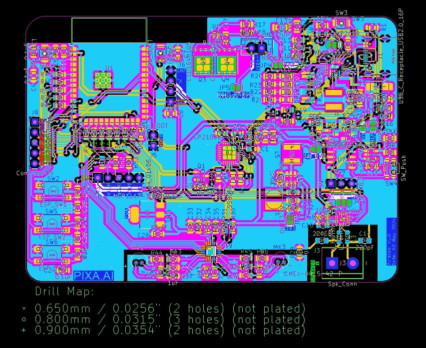

Specifications
Automated Checks
8+
Automated DFM checks per upload
Engineer Review
24 h
Human DFM engineer review
Cost
$0
Free report, no order obligation
Judged Against
Your spec
Reviewed vs your process, not one fab default
Experience
16+ yrs
EMS & turnkey manufacturing
Path to Build
Fab + Assembly
One turnkey path from report to build
01 / DFM Checks
What Our DFM Analysis Checks — Trace/Space to Annular Ring
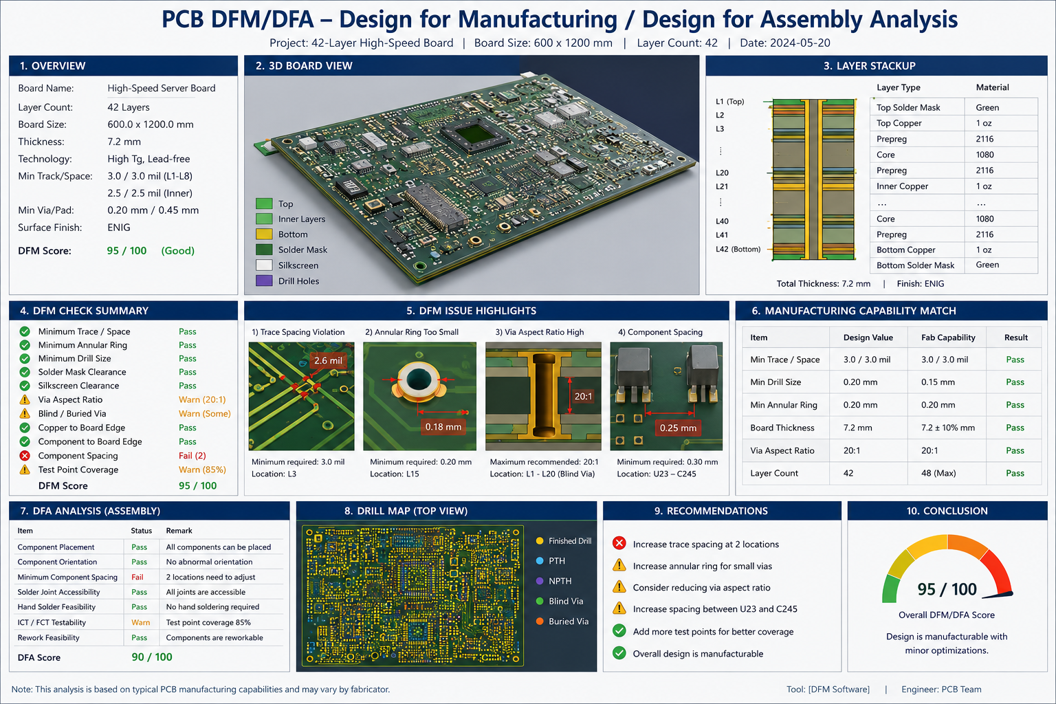
Every upload runs a design rule check against the same rule set a manufacturer uses to accept or reject a job, read from your Gerber and drill files, to verify the layout before it enters the manufacturing process. Here is what each check looks at and the limit it is measured against — real numbers a PCB designer can act on, not a red/yellow/green guess.
| Check | What it catches | Typical limit measured against |
|---|---|---|
| Trace width & spacing | Traces or gaps too fine to etch reliably, acid traps | Standard fab capability ~0.1 mm / 4 mil min (tighter on advanced lines) |
| Drill & annular ring | Pads that break out from the hole after drill tolerance | Min external annular ring ~0.05 mm / 2 mil, IPC-6012 Class 2 (Class 3 tighter) |
| Copper-to-edge clearance | Copper too close to the board edge to route safely | Typical 0.2–0.3 mm depending on edge process |
| Solder mask clearance & slivers | Mask pulling onto pads, thin mask dams that flake off | Pad-to-mask 2–7 mil (DRC default ~4 mil); min mask dam/web ~4 mil |
| Silkscreen legibility | Silk on pads, text too small to print clearly | Min line width / height per fab; no silk over exposed copper |
| Minimum hole & aspect ratio | Holes too small or boards too thick to plate through | Min finished hole + aspect ratio for the stack-up |
| Netlist — shorts & opens | Unintended shorts or broken nets in the copper | Compared against the IPC netlist where supplied |
| Component placement (DFA) | Courtyard overlap, polarity, footprint-to-part fit | Needs BOM + centroid data (see note) |
02 / Engineering Note
What Gerbers Can and Can’t Tell Us
Gerber and drill files describe copper, mask, silkscreen and holes, so fabrication DFM runs cleanly from them. They carry no bill of materials and no XY/centroid data, which means assembly checks — courtyard spacing, polarity, footprint-to-part fit — cannot be done from Gerbers alone. For a full design for assembly review, send your BOM and centroid file, ideally as ODB++ or IPC-2581, and our engineer covers both fabrication and assembly in one pass.
01 / How DFM Gets Done
Instant Auto-Tool vs Manual Service vs PCBark’s Hybrid DFM
There are three ways to have your board evaluated, and not all are equal. The real difference for the designer, when the stakes are high, isn’t speed – it’s who actually determines which “flags” are real. Let’s run down the options as if a report just dropped into your email.
| Instant free tool | Manual file-check service | PCBark hybrid | |
|---|---|---|---|
| Speed | Seconds | Days, often opaque | Automated on upload + engineer in 24 h |
| False-positive handling | None — raw flag dump | Varies | Engineer filters noise from real blockers |
| Judged against | One fab’s default rules | That shop’s spec | Your target process |
| Human interpretation | No | Sometimes | Yes — a DFM engineer, every time |
| Assembly (DFA) | Rare | Sometimes | Yes, with BOM + centroid |
| Path to build | None | Limited | Turnkey fab + assembly |
| Cost | Free | Free or paid | Free, no obligation |
02 / Why It Matters
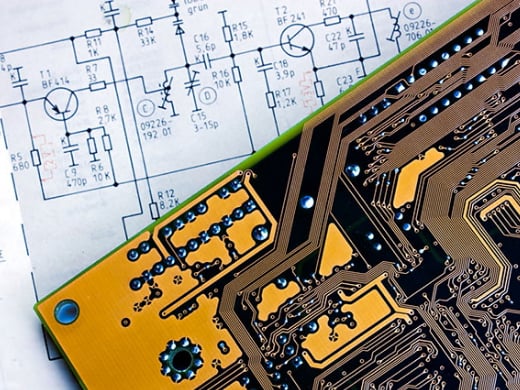
A Script Flags — an Engineer Decides
A quick DFM tool — or the design rule check built into your PCB design tool — is genuinely useful for a fast sanity pass while you are still routing. What it cannot do is tell you that thirty of its forty warnings are an artifact of grading your board against a fabricator you are not even using. A real DFM review still leans on an experienced engineer to catch geometric issues, standards violations and process-specific risk — that is how manufacturable boards actually get signed off, and it is the part a script does not replace. The goal is simple: confirm your PCB design has the manufacturability to clear the manufacturing process the first time, so PCB designers ship boards instead of chasing avoidable respins.
Curious how many of your “violations” are real?
Get a free engineer-reviewed DFM report →Overview
PCB DFM Analysis at PCBark
01 / How It Works
From Gerber Upload to Manufacturable Board — How It Works
The goal of any review is to take any problems at the end of your process and move them to the front. You’re never more than one step away from an engineer here.
Upload your Gerbers
Send your Gerber and drill design files (a ZIP works). Add your BOM and centroid for assembly DFA.
Automated DFM scan
The rule set checks trace/space, drill, annular ring, copper-to-edge, mask, silk and netlist in minutes.
24-hour engineer review
A DFM engineer reads the flags against your target process, drops the noise, and ranks what to fix and why.
Manufacturable report
You get a clear, prioritized report — and an optional turnkey path to fabricate and assemble with PCBark.
02 / Why Early Catches Pay
A design error caught at layout, at fabrication, and in the field. DFM analysis pulls your fix to the cheapest point on that curve — before tooling, parts and weeks of queue time are spent.
QUALIFIED 1:10:100 cost-of-change is a general cost-of-quality framework; prototype respins are industry-cited at roughly $8,000 per spin plus weeks of delay. Figures are planning references, not a per-board guarantee.
Whether you build with us or not, the math is the same. A rule violation found while your layout is still editable costs a few minutes to fix. That same violation found after fabrication costs a respin and the calendar that comes with it; found in the field it costs a recall conversation. Moving that catch earlier is the entire return on a DFM check — and it is why an engineer-reviewed report beats a raw flag dump you still have to triage yourself.
Want the report tied to a real build estimate?
Send your design for a quote-ready review →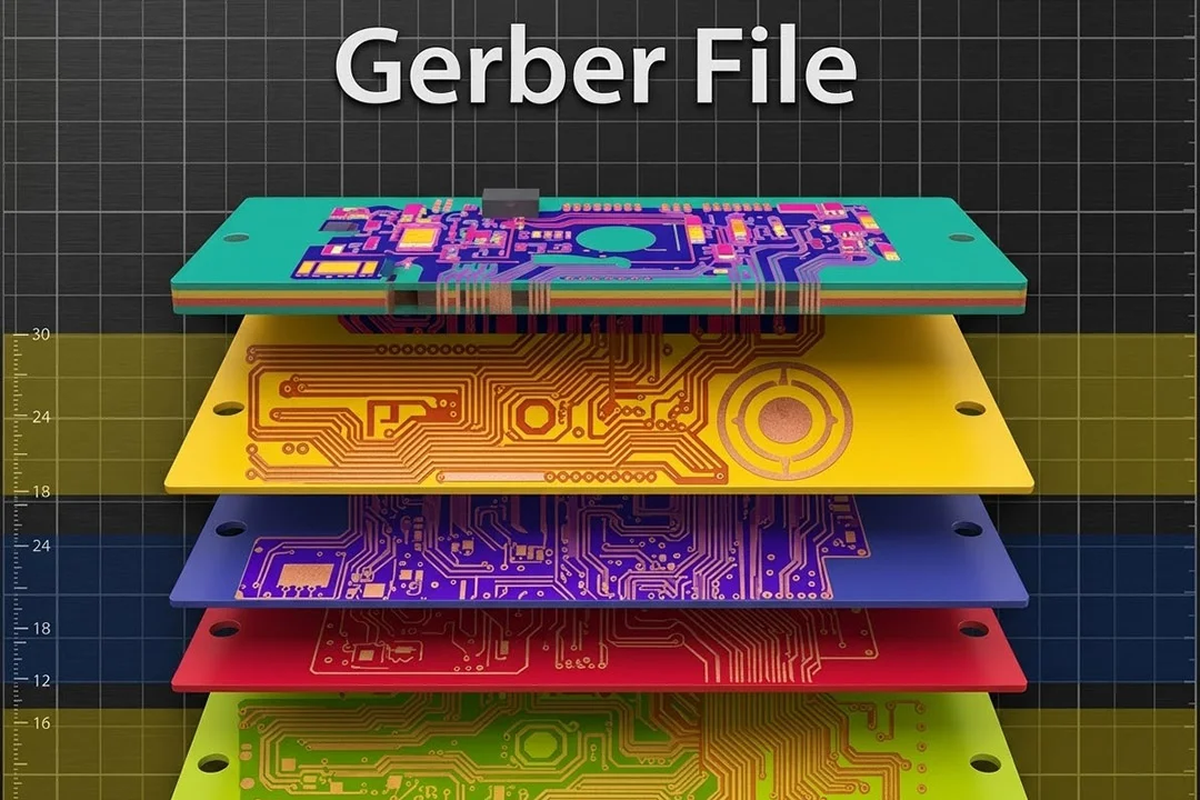
01 / Manufacturing Constraints
Checked Against Real Manufacturing Constraints — IPC & PCBark’s EMS Backbone
Sound PCB design for manufacturing rests on real limits, not guesses, so every check traces to a published IPC standard or to what our own lines actually run. Annular ring and copper acceptance follow IPC-6012, PCB layout and design for manufacturing limits trace to IPC-2221, land patterns to IPC-7351, and finished-assembly acceptance to IPC-A-610. Your build class is agreed before production, so the same board is judged the same way on the first article and the ten-thousandth.
IPC-2221
Generic PCB Design Standard
IPC-6012
Rigid Board Qualification
IPC-7351
Land Pattern Standard
IPC-A-610
Assembly Acceptance
ISO 9001
Quality Management System
02 / The Manufacturer Behind It
A Rule on Paper vs a Rule That Holds on the Line
What makes the review more than a rulebook lookup is the manufacturer behind it. As a PCB manufacturer, PCBark brings design and manufacturing together under one roof: 16-plus years of EMS work across 500,000 m² of annual capacity, with fabrication, assembly and functional testing in-house. That engineer has built thousands of boards like yours and knows where this fabricator’s real edge is — the difference between a rule on paper and a rule that holds on the line. Applying these manufacturing best practices early keeps your product design on schedule and your PCB manufacturing yield high.
Need the review against a specific IPC class?
Tell us your target class and process →01 / Your Free DFM Report
Getting Your Free DFM Report — What’s Included, Turnaround & Next Steps
The report itself is free and carries no obligation to order. You upload, you get the automated results, and within 24 hours a DFM engineer sends back a prioritized write-up: the real blockers, the flags you can ignore, and the fixes worth making before release. We are upfront about why it is free — catching a problem now beats building a board that fails, and a clear, honest review is how designers decide we are worth the build.
What Drives the Quote
There is no flat price for the fabrication and PCBA assembly that may follow, because the cost is driven by your design, not a list. Knowing the factors up front makes your RFQ faster and your quote accurate:
Board complexity
Layer count, board size and fine-pitch content set fabrication effort.
IPC acceptance class
Class 2 versus Class 3 changes acceptance limits and documentation.
Assembly scope
SMT, through-hole and BGA content, and whether you need DFA plus build.
Volume
Prototype, bridge or production quantity drives tooling and unit economics.
Send the Assembly Data Too
For assembly orders, customers submit BOM and centroid details along with their Gerbers, preferably ODB++ or IPC-2581 for efficient checking and component verification even after the fabrication analysis.
Submit desired files and receive an updated report within 24 hours; to have a specific quotation for assembly and fabrication, supply the relevant target volume and class.
DFM Tools
PCB DFM & Design Tools
Annular Ring & Minimum Hole Checker
Check the external annular ring left after drill registration against your IPC class.
PCB Trace Width Calculator
Size minimum copper width for a target current and temperature rise (IPC-2221).
Via Aspect Ratio Checker
Compare board-thickness-to-hole ratio against standard and advanced plating limits.
DFM Readiness Self-Check
Tick what your design covers and score how close it is to a clean fabrication release.
Frequently Asked Questions
PCB DFM Analysis FAQ
What is PCB DFM analysis, and what does PCBark’s free check include?
PCB DFM analysis checks your design against real fabrication and assembly limits before production. Our free check runs automated rules on your Gerber and drill files — trace and space, drill and annular ring, copper-to-edge, solder mask, silkscreen, minimum hole and netlist — and a DFM engineer then reviews the results within 24 hours and tells you which flags actually matter for your build.
Are Gerber files enough for a complete DFM analysis?
For fabrication DFM, yes — Gerber and drill files describe copper, mask, silkscreen and holes. For assembly checks they fall short, because they carry no BOM and no centroid data. Send those too, ideally as ODB++ or IPC-2581.
How is your free DFM check different from an instant one-click tool?
Instant tools grade your board against one fabricator’s default rule set, so they over-flag — a screen full of annular ring warnings you can safely ignore is the classic example, and sorting the two real blockers from the forty that do not matter eats your afternoon. We run that automated pass as well, but a DFM engineer then reads the flags against your actual target process, drops the noise, and hands you a prioritized report. You get judgement, not a raw dump — and that judgement is what keeps a clean-looking board from shipping unbuildable.
Does the analysis cover assembly (DFA), or only fabrication?
Both, once you share the data. Fabrication DFM runs from your Gerbers; design for assembly needs the BOM and centroid. Because PCBark builds the board as a turnkey EMS, our engineer reviews fabrication and assembly together, so a design that clears the file check is also buildable on the line.
When in my design process should I run a DFM check?
Twice. Run a quick check while your layout is still editable and changes cost minutes, then a full check before you release for fabrication. Catching a fault early sits at the cheap end of the 1:10:100 curve.
Is the free DFM report really free, with no order obligation?
Completely free, with no obligation to order. Take the report and build anywhere. Designers who get a clear, honest review tend to come back for the build — that is the whole bet.
How fast is the turnaround, and who reviews my board?
Automated checks run the moment you upload; a DFM engineer finishes the human review within 24 hours. A real engineer — not a script — reads the flags against your target process, separates true blockers from noise, and writes up what to fix and why.

How It Works
How We Actually Run a DFM Review
The automated rule check comes first when you upload Gerbers, then an engineer who reads annular ring, solder mask sliver and IPC-7351 land pattern errors against your specific target process, as a high proportion of the red flags on an incoming board are triggered against the generic defaults of just one fabricator and would not actually stop one of our builds.
QUALIFIED IPC limits cited here apply as published; respin times and failure figures are industry references, not guaranteed per-board costs.
Free DFM Analysis
Upload Gerbers Now for a PCB DFM Analysis
Upload Gerbers now for a PCB DFM analysis. Get automated checks, an engineer-reviewed report, and 24-hour turnaround. No order commitment.
- Automated checks
- Engineer-reviewed report
- 24-hour turnaround
- No order commitment