Get in touch with PCBark Company

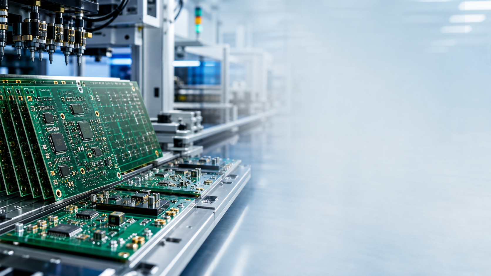
PCB Fabrication · Assembly · Turnkey EMS
Custom PCB Manufacturer,
PCB Fabrication & Assembly
Turnkey electronics manufacturing from prototype to volume – 16+ years in EMS, 500,000 m² of annual capacity, boards built to IPC Class 2 and Class 3 acceptance.
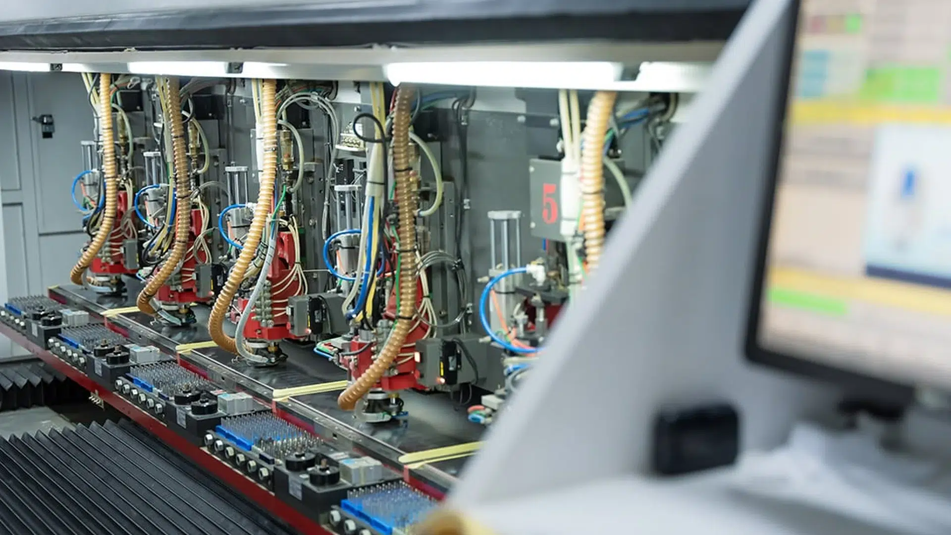
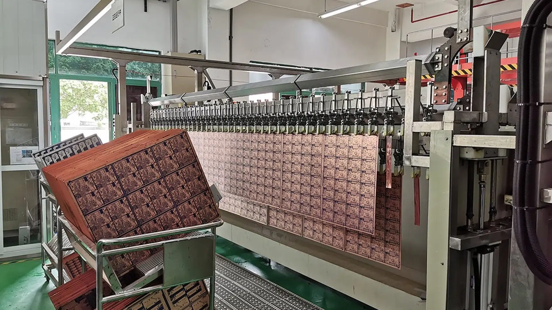
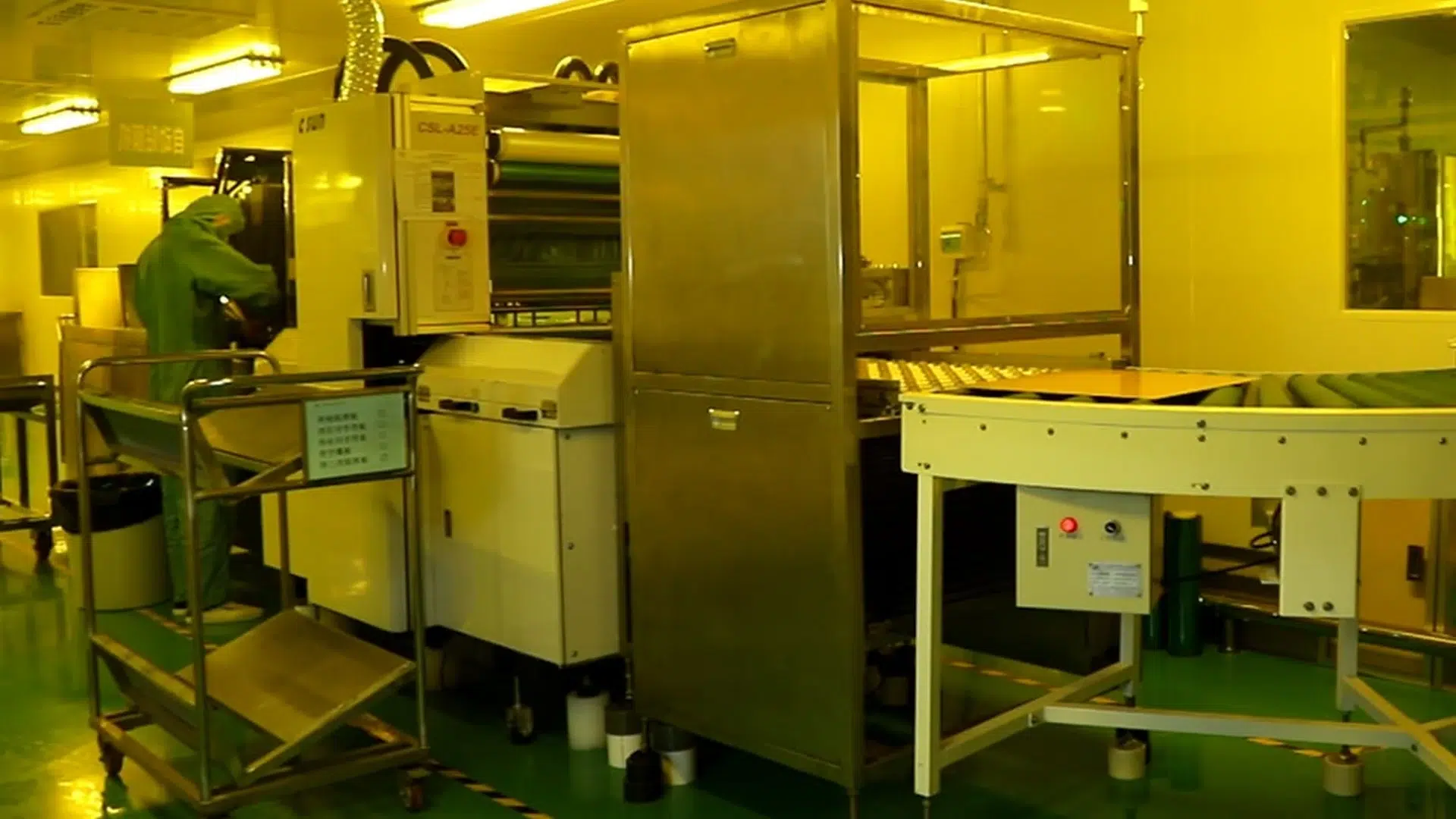
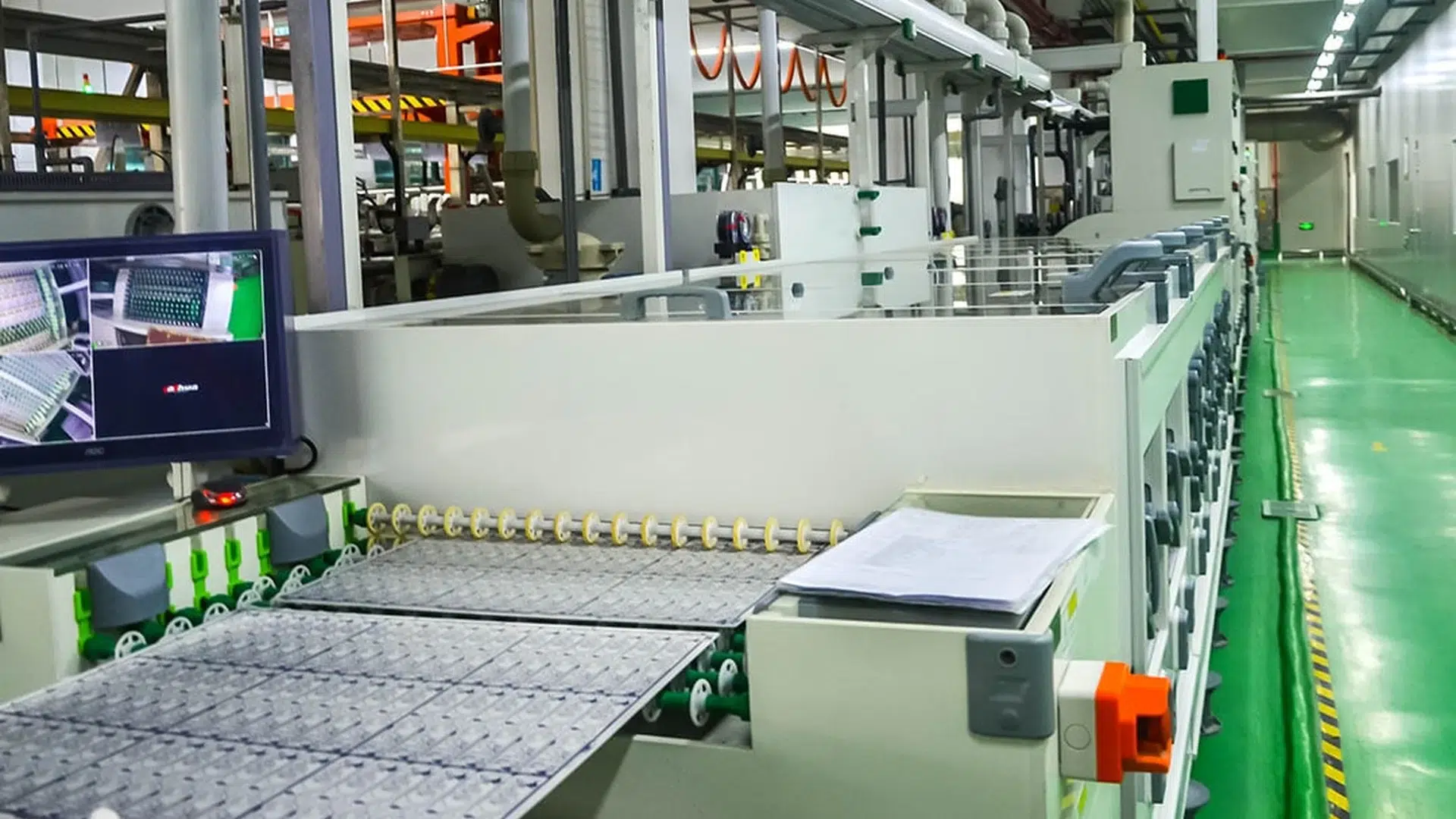
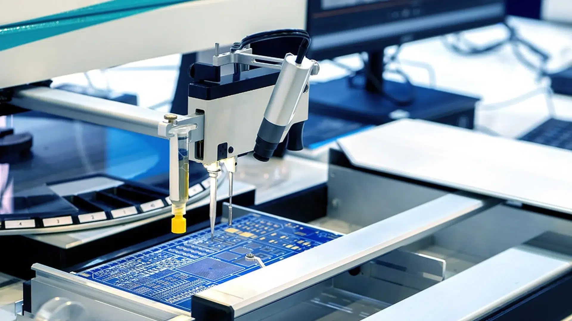
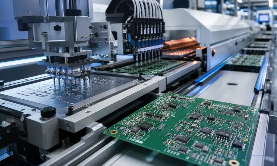
PCBark is a custom pcb manufacturer and full-service electronics manufacturing services partner. We fabricate printed circuit boards from 1 to 42 layers in six different substrates, source electronic components based on your BOM, perform SMT and through-hole assembly, and conduct functional tests – one supplier and one quality system from gerber file to the delivered board.
- 16+ Years in EMS
- 500,000 m² Annual PCB capacity
- 1–42 Layer count range
- Class 2 & 3 IPC build discipline
PCB Manufacturing Capabilities
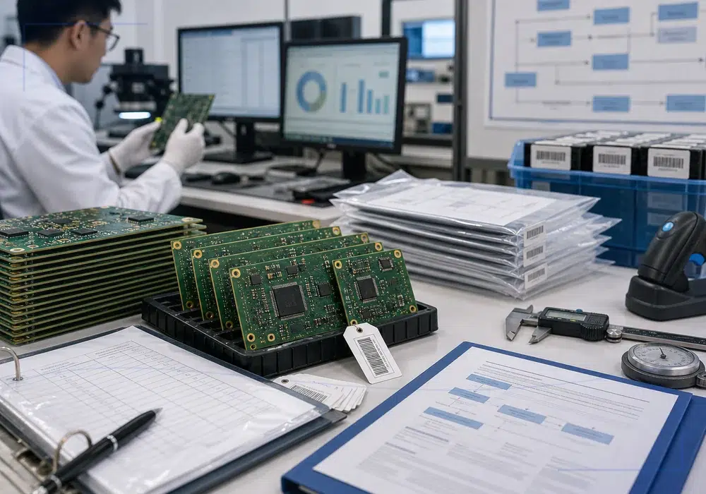
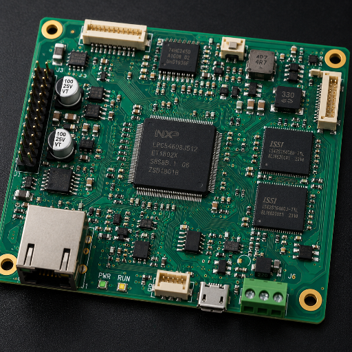
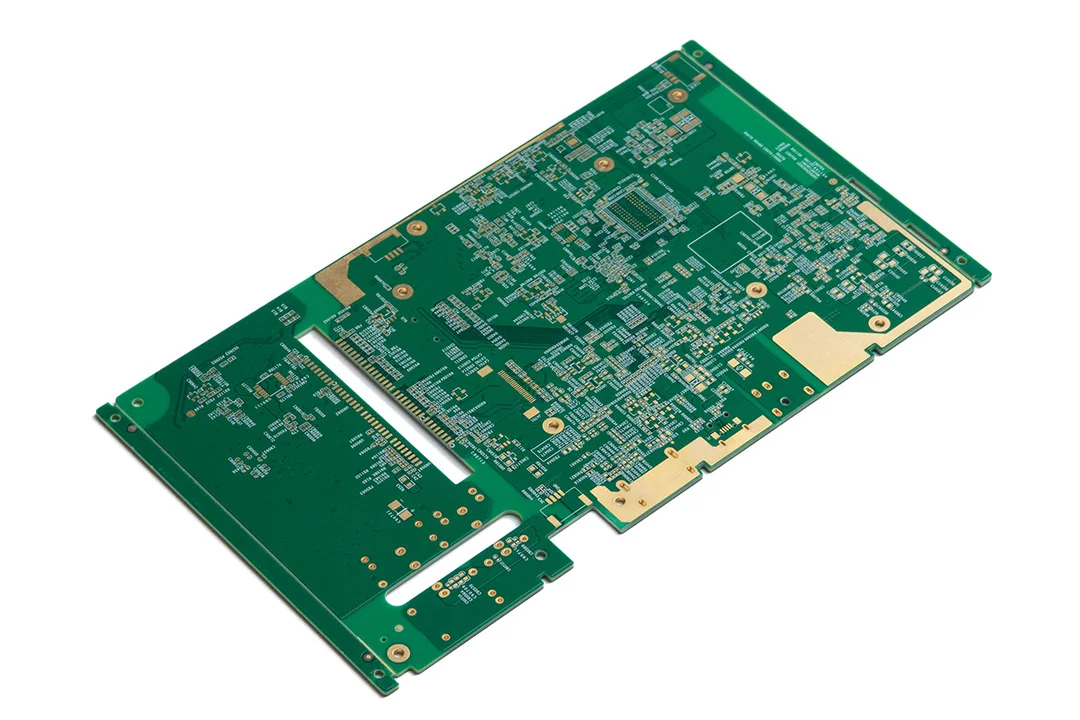
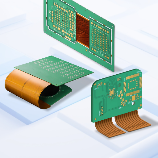
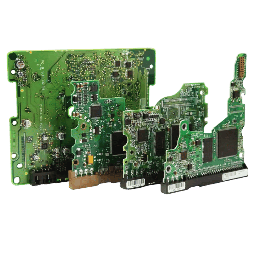
Engineered for reliability. We provide 1–42 layer fabrication across six advanced substrate families, integrating seamlessly into your hardware product development roadmap.
PCB Assembly
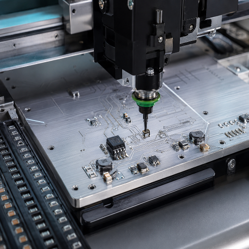
Turnkey PCBA services spanning surface mount (SMT), through-hole (THT), and mixed technologies.
View Assembly Services →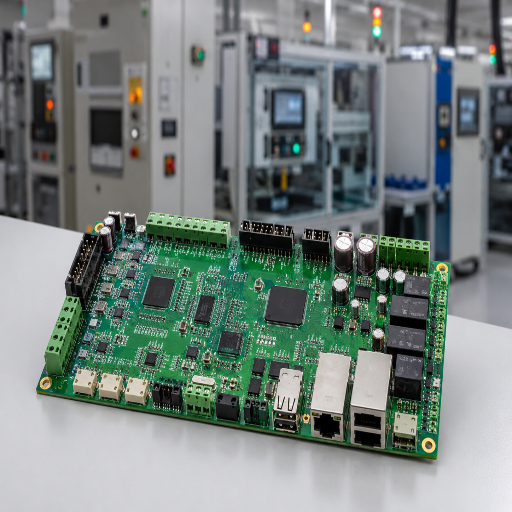
Industries We Serve
High-reliability boards designed for Automotive, Medical, Aerospace, and Industrial control sectors.
View Industry Solutions →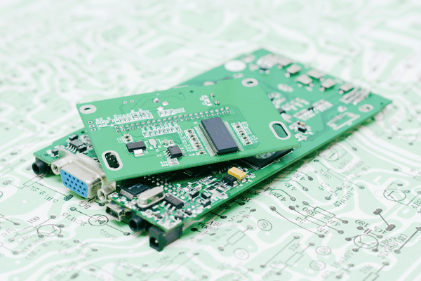
Full Capabilities
Explore comprehensive manufacturing limits, material tolerances, and stringent quality control standards.
Review Full Capabilities →PCB Fabrication and Assembly Under One Roof: SMT to Box Build
Turnkey PCB Assembly
BOM sourcing with itemized parts pricing
Fab + assembly + test, one PO
Turnkey →
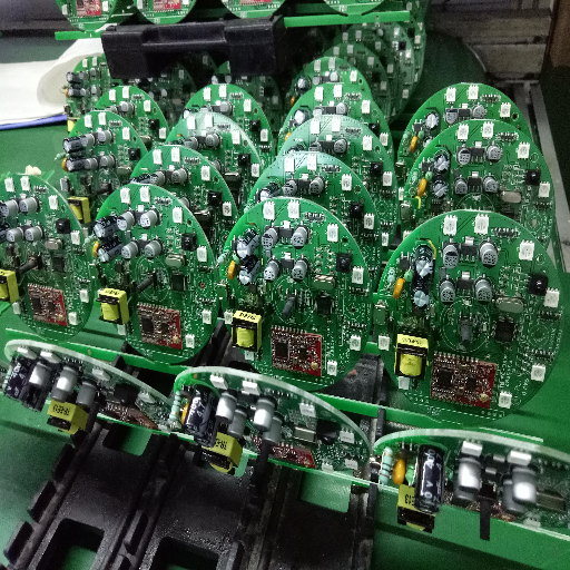
Quick-Turn Assembly
Expedited builds, transparent queue
DFM check before the clock start
Quick-turn →
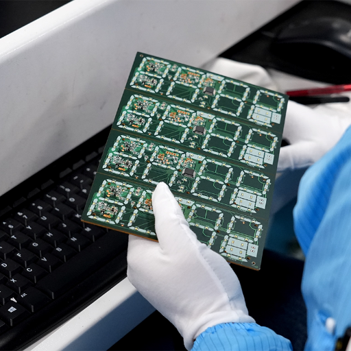
Prototype PCB Assembly
No-MOQ engineering builds
Same line discipline as production
Prototype →
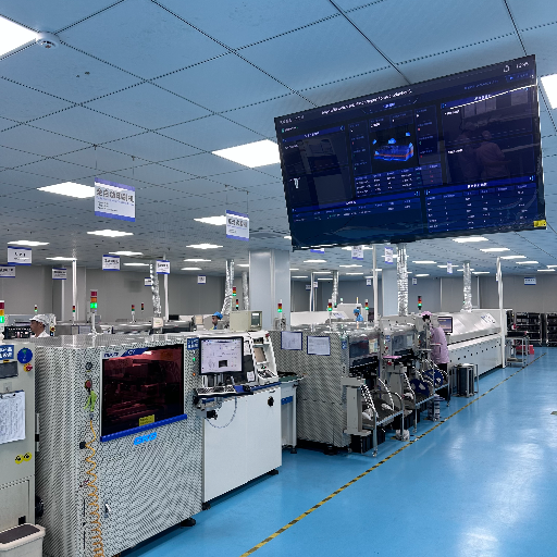
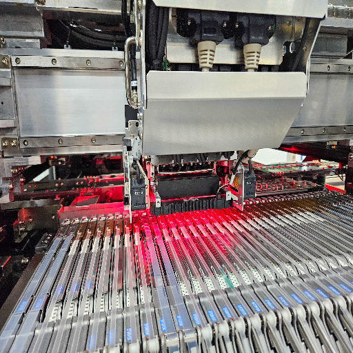
SMT Assembly
Fine-pitch surface mount placement
AOI on 100% of Class 3 work
SMT →
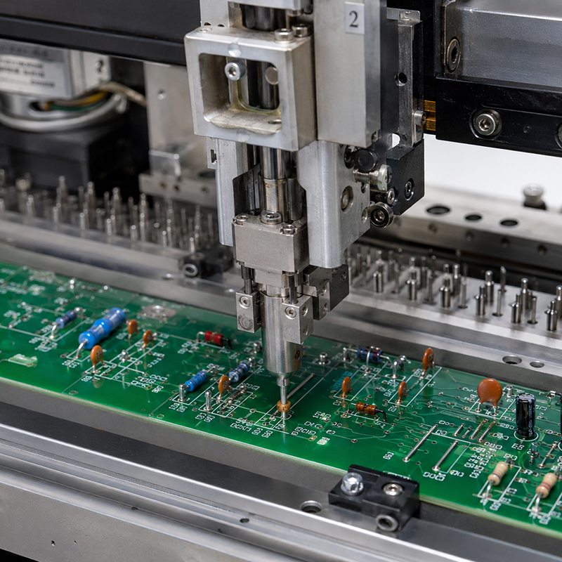
Through-Hole / DIP
Wave and selective soldering
Mixed-technology boards
Through-hole →
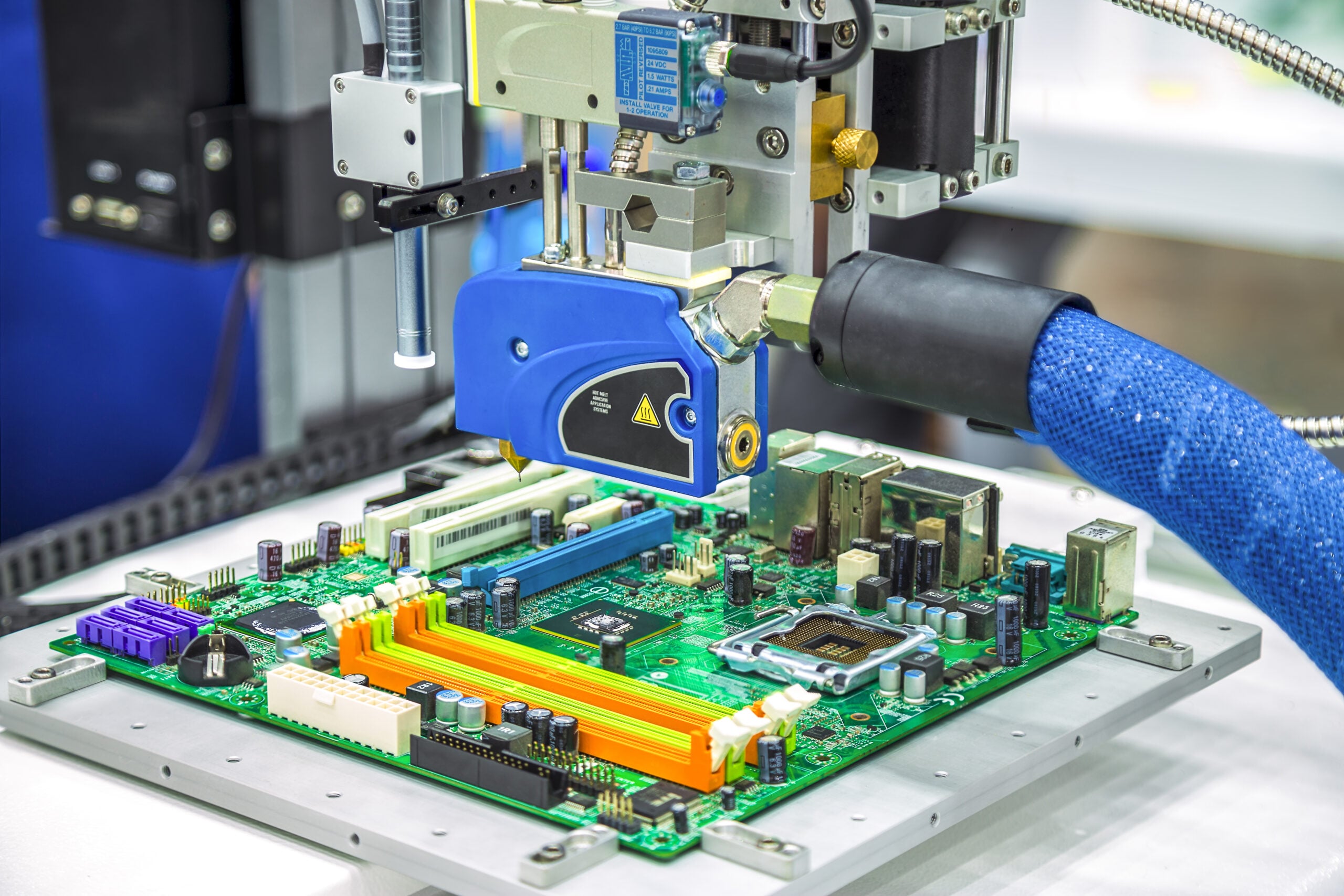
BGA Assembly
X-ray void inspection
Rework station with profile control
BGA →
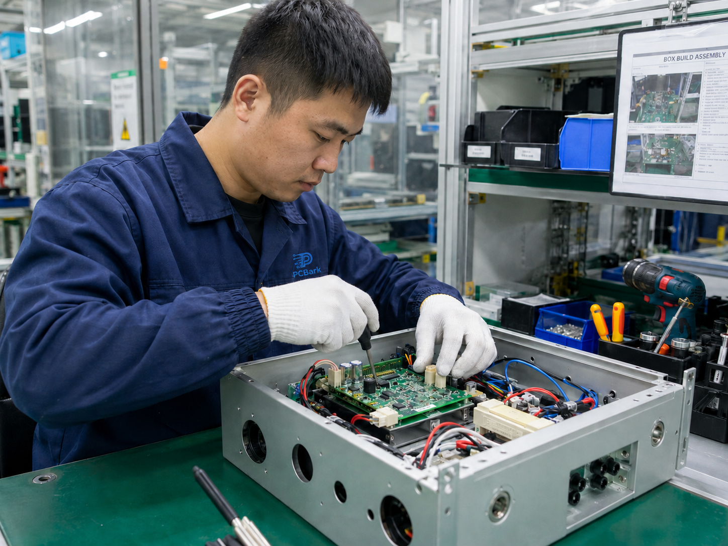
Box Build / Final Assembly
Enclosure, cabling, firmware load
Functional test to your spec
Box build →
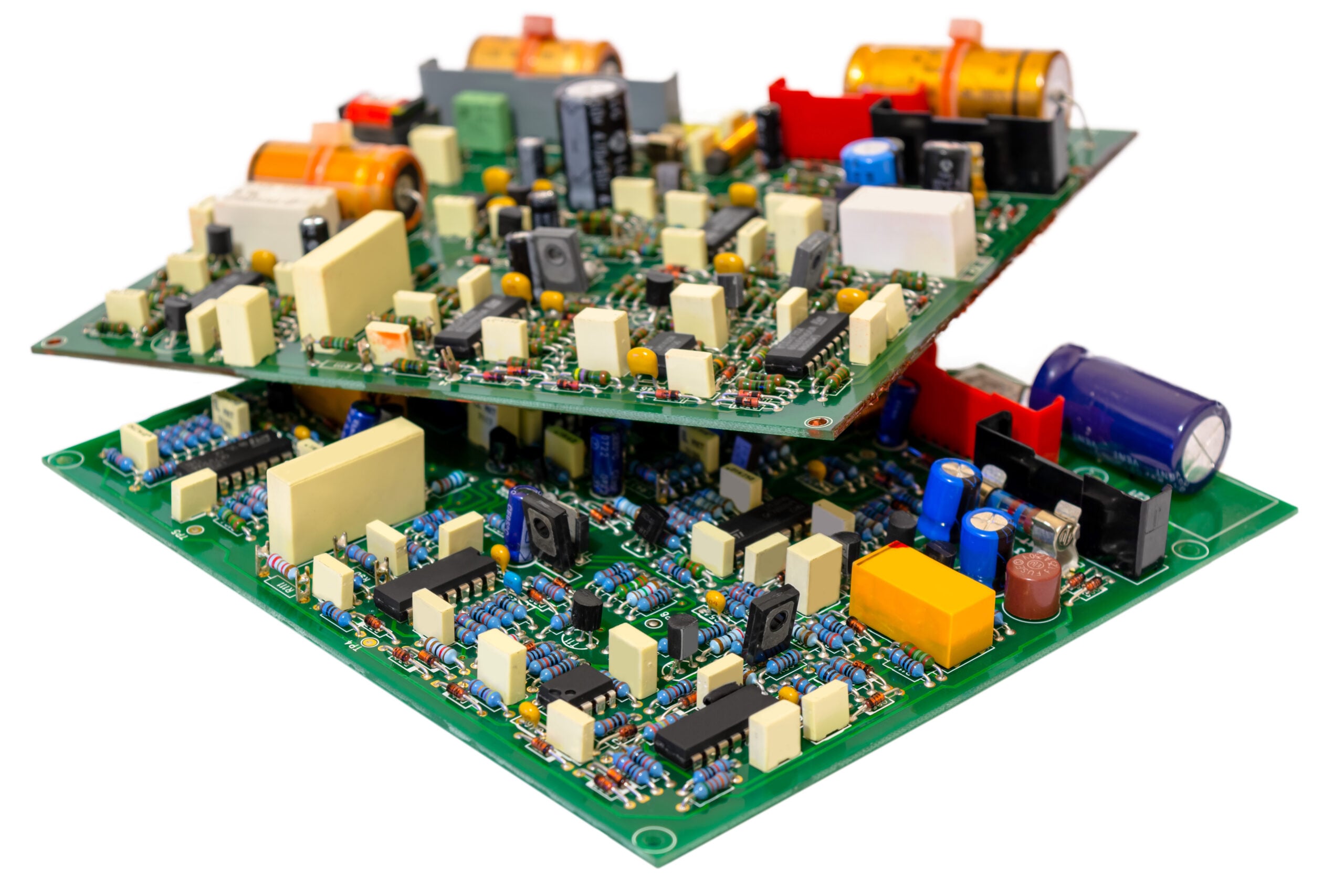
Circuit Card Assembly
High-reliability CCA builds
Full lot and component traceability
CCA →
Quick-Turn Platform or EMS Partner? The 9-Line Sourcing Decision
Engineers are fairly honest about the big online platforms: the bare board quality at prototype volumes is good stuff, and nothing will beat the $2 commodity proto board for price. The complaints that populate the engineering community begin later-repeat customers report that every time they order a batch they get a different outcome, consignments disappear within the platform warehouse, and defect reports are met with the advice, “de-solder the chips yourself.” The platform’s failure mode isn’t the first 5 boards-it’s the 5,000th.
Shortlists of the top PCB manufacturers don’t typically say this plainly, so here’s the honest version: for five 2-layer test boards, a quick-turn platform is a solid choice. That isn’t true once production, compliance or complex PCB custom work enters the mix.
| Decision Line | Quick-Turn Platform | PCBark (EMS Partner) |
|---|---|---|
| Built for | Prototype / hobby / low volume | NPI through mass production |
| MOQ | From 1–5 pcs | No-MOQ protos; scales to volume |
| DFM review | Automated rule check | Engineer-led review before fab starts |
| Quality grade | IPC Class 2 default | IPC Class 2 & Class 3 builds to spec |
| Batch consistency | Reorder variation top complaint | Locked process recipe + lot traceability |
| Parts sourcing | Own-stock, ~2× markup reported | Itemized BOM pricing, alternates approved |
| Engineering contact | Ticket queue | Named engineer, RFQ to ramp |
| IP handling | Standard terms | NDA on request; file partitioning |
| When it goes wrong | Dispute process, refund at best | 8D-style root cause, rework, and a person |
Lowest quote ≠ lowest cost
EMS practitioners document projects where the lowest unit price ended up about 20% more expensive once all landed costs were considered — freight, duties, rework, and scrapped assemblies. A failed board costs the board, the parts on it, and the schedule.
Landed-cost field reports and industry cost analyses; figures vary by project.
Tariffs only sharpen the calculation. There’s a 25% Section 301 duty under the USTR’s 2024 four-year review on bare printed circuit boards of Chinese origin. The only surviving bare-board exemptions include very specific, flat rigid FR-4 2- and 4-layer types that the platforms build-an exemption which is valid through late 2026. Multilayer and HDI boards fall outside those exemptions, and finished assemblies are classified separately under their own tariff headings. This is why we provide landed cost context, rather than just the EXW price; when a supplier omits the duty from a line item, it isn’t cheaper-it’s just stealthy.
A PCB contract manufacturer takes fabrication, component sourcing, assembly, and testing under a single contract and a single quality system. Instead of juggling relationships with a board house, component vendor and assembly shop, the OEM hands over gerber files and a bill of materials, and receives fully tested boards with single-point responsibility for cost, schedule and quality.
Industries We Serve: From Industrial Control to Medical and IoT
SYSTEM LOG // ORBITAL NETWORK
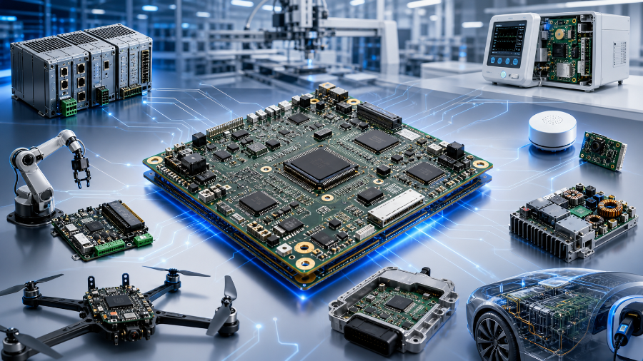
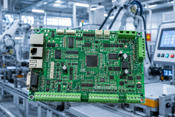
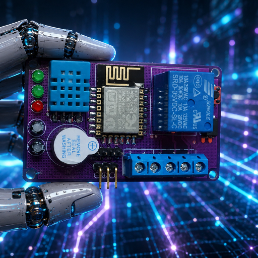
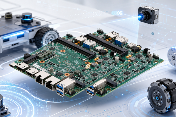
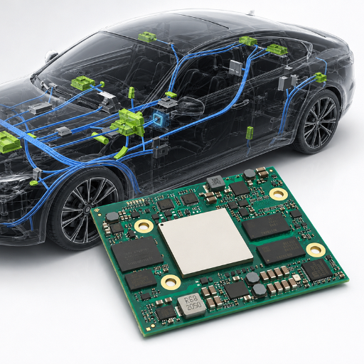
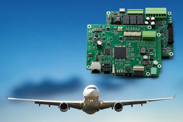
Industry brand names in the supplier’s portfolio don’t matter until they are mapped to specific product requirements. For us, mapping to process requirements is clear: medical electronics conform to IPC Class 3 acceptance and component traceability requirements because the FDA requires that documentation in its 510(k) submission process and audits. For automotive and industrial automation products, it means we adhere to the IATF 16949-standard of process controls and provide serialized lot traceability. We produce HDI boards for robotics and drone applications where weight is at a premium. We serve the smart home and IoT market where affordable, consistent multilayer production is essential. For telecommunications hardware, adherence to impedance discipline is king. And while we support commercial aerospace electronics under Class 3 rigor, we do not bid on defense or export-controlled opportunities.

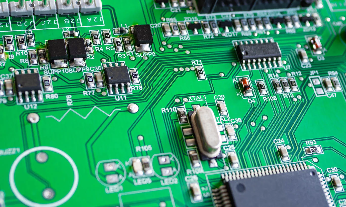
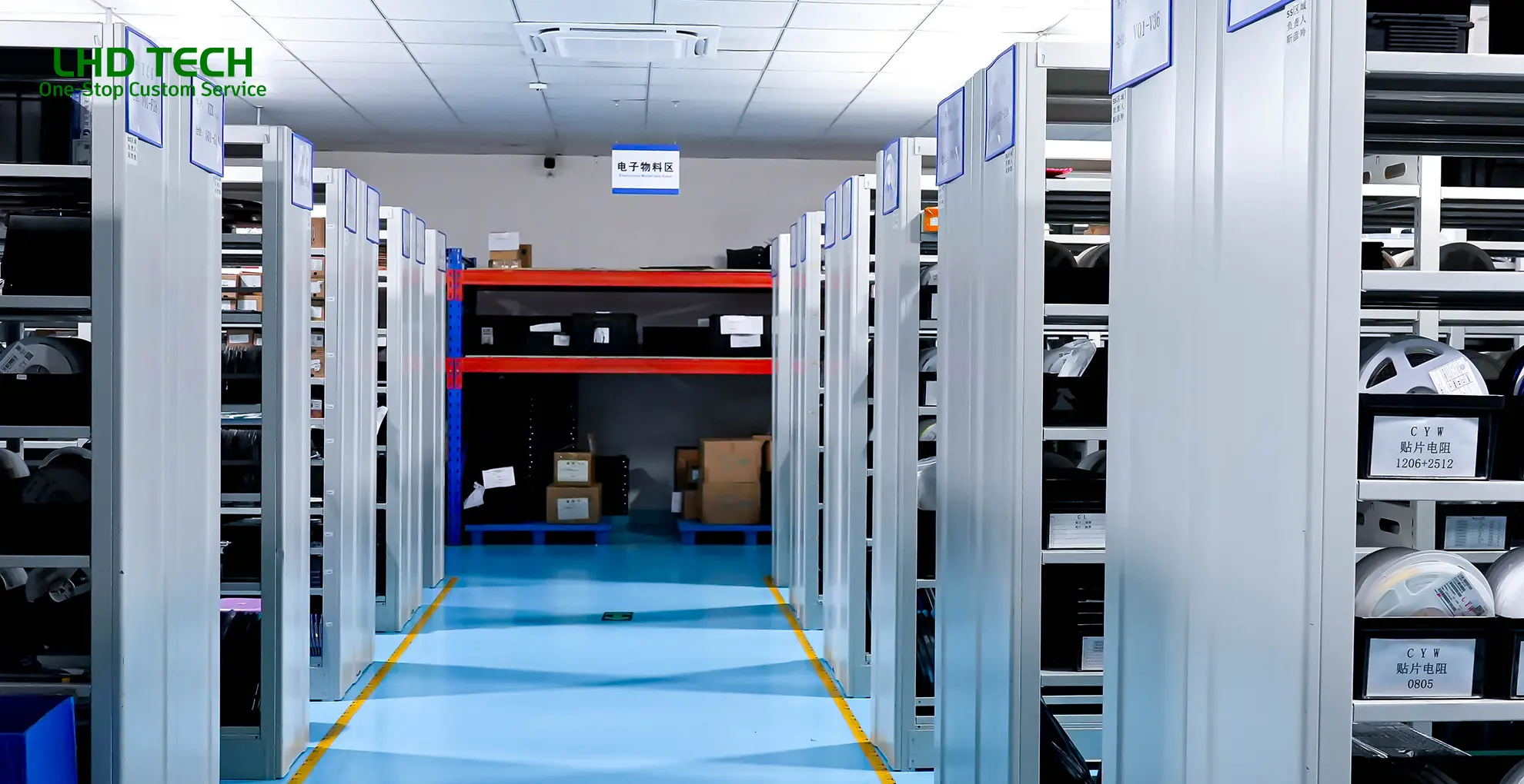
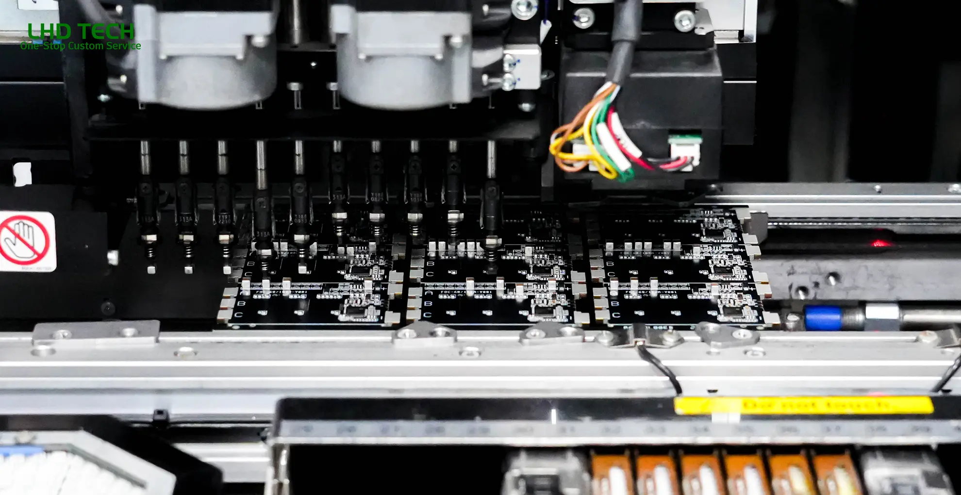
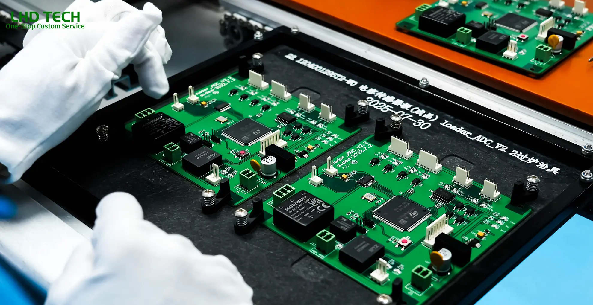
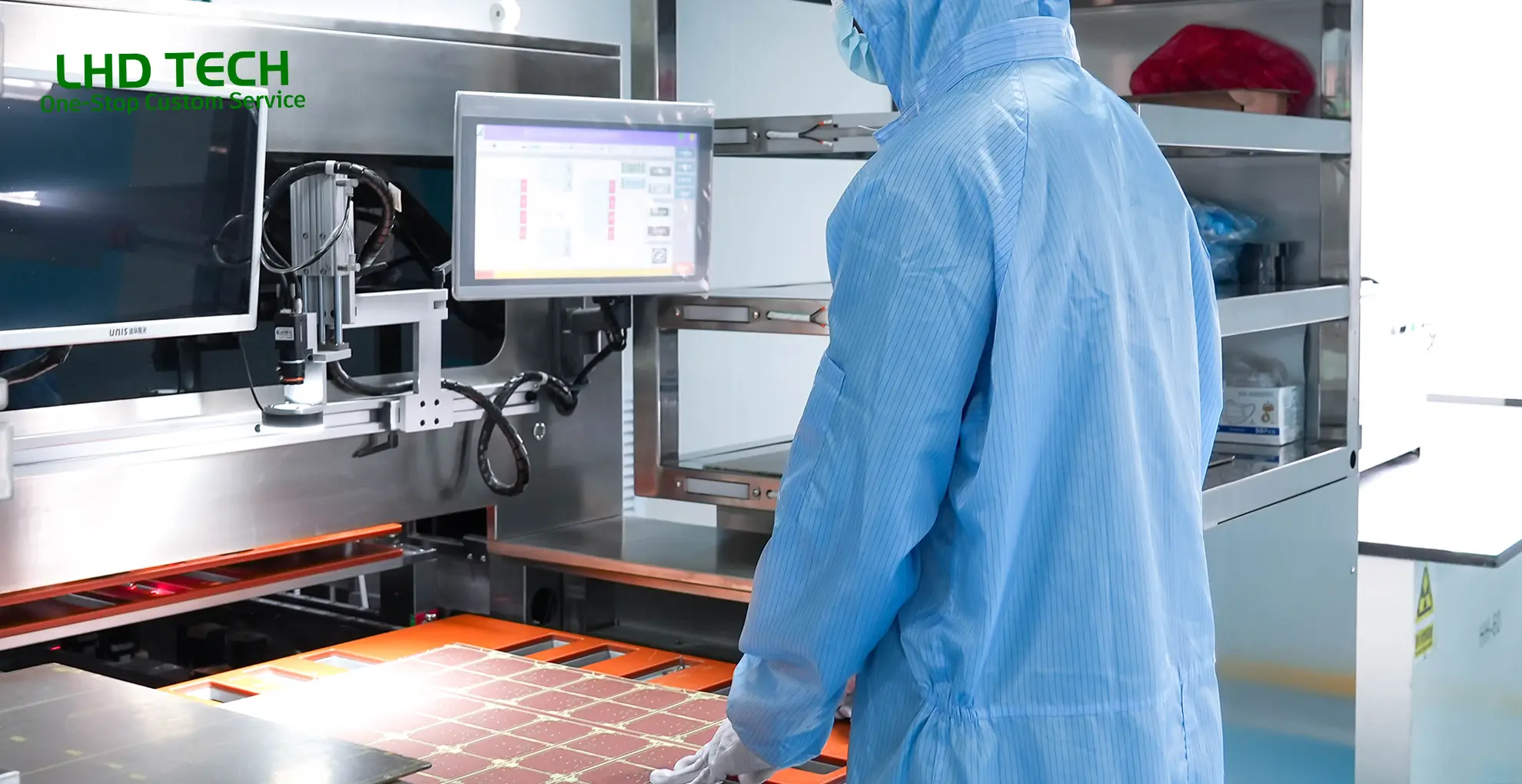
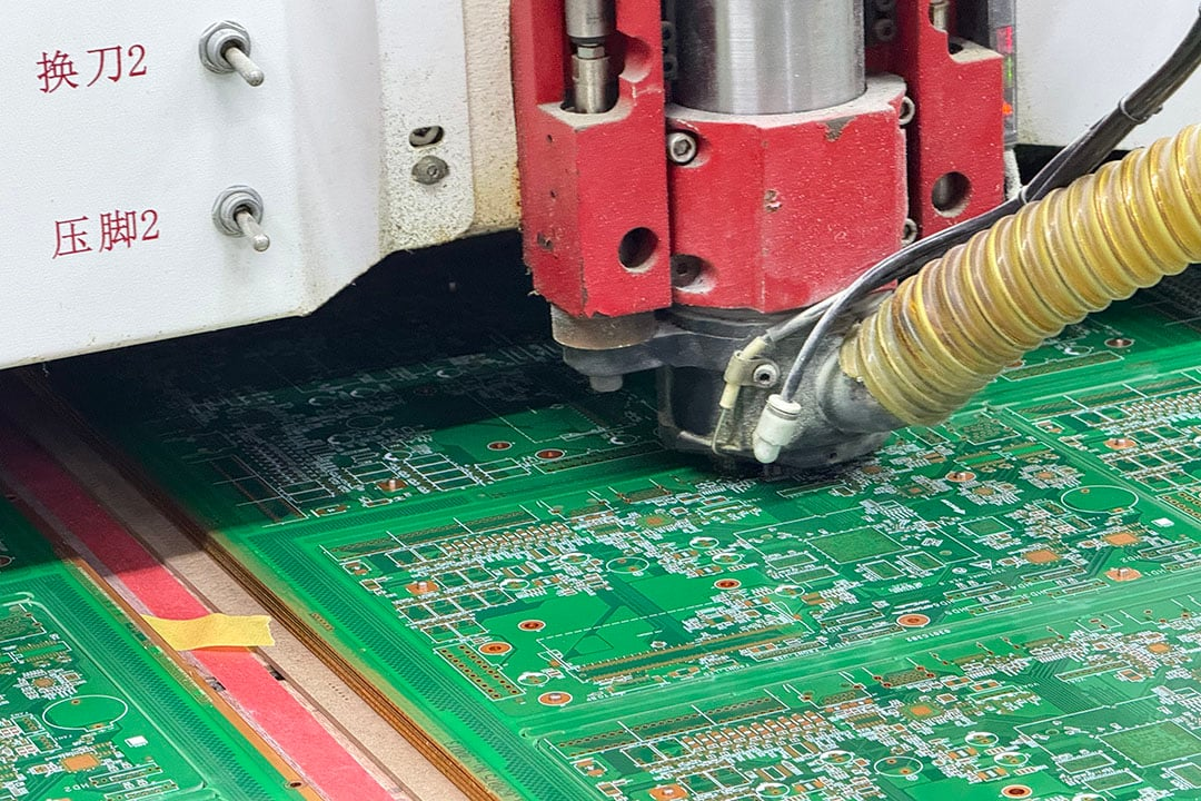
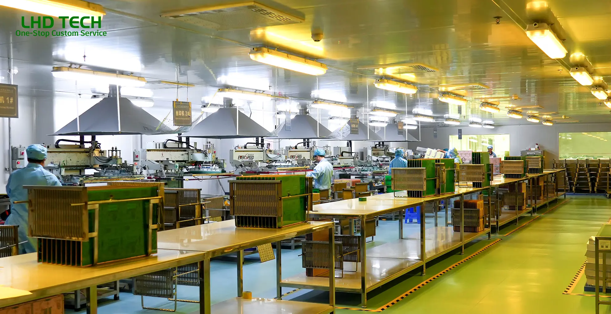
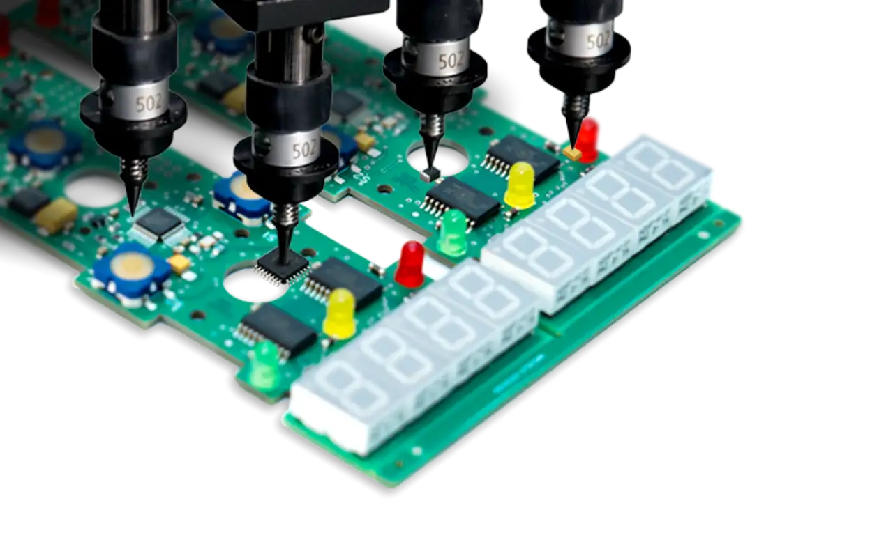
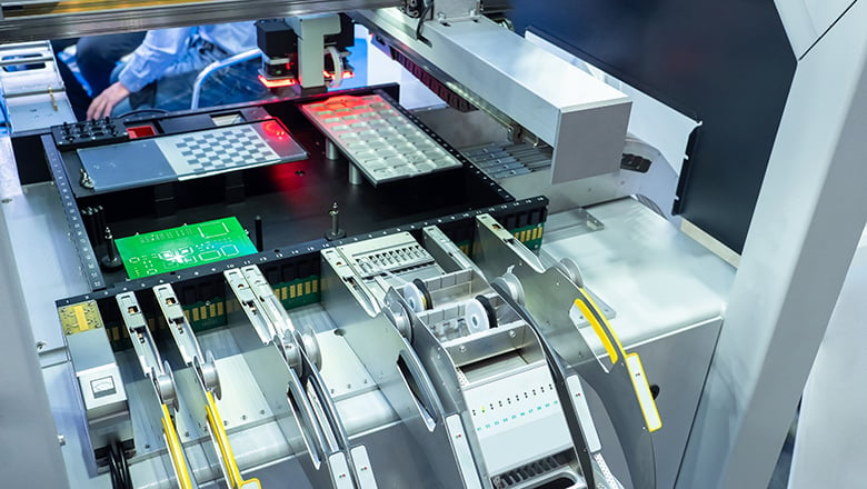
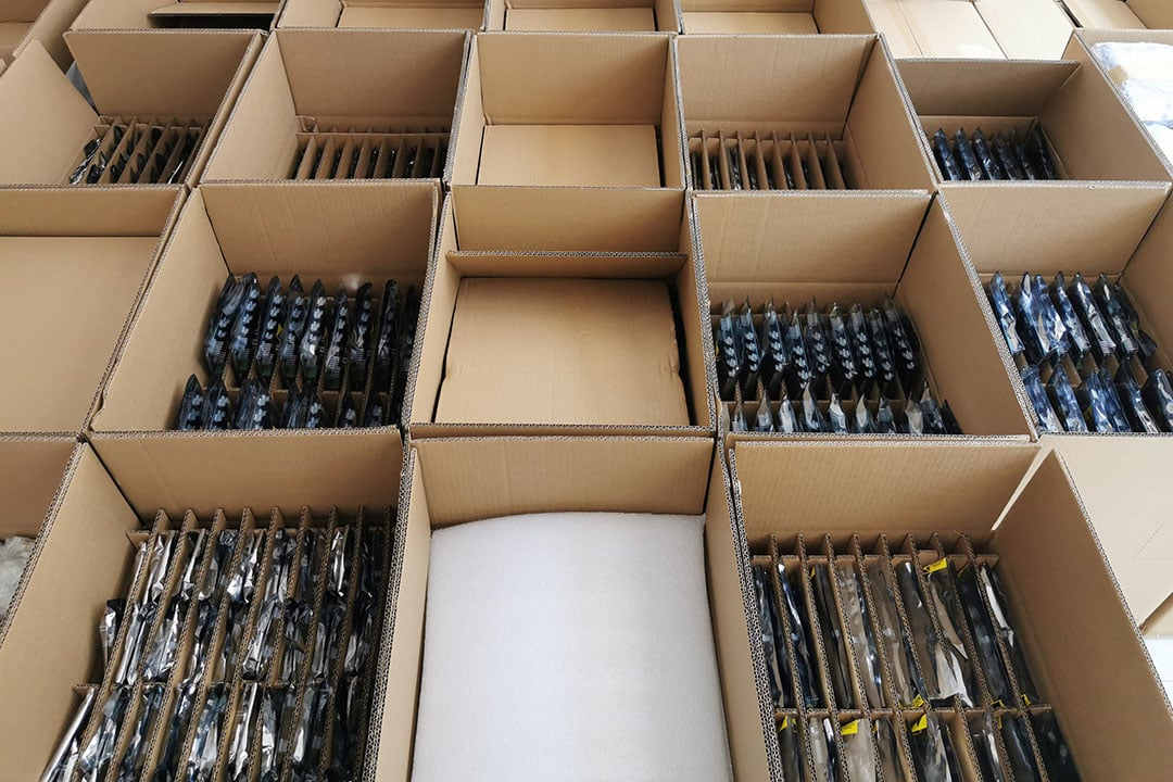
State-of-the-Art PCB Manufacturing Facilities
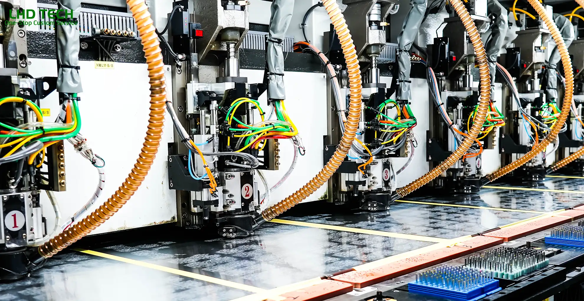
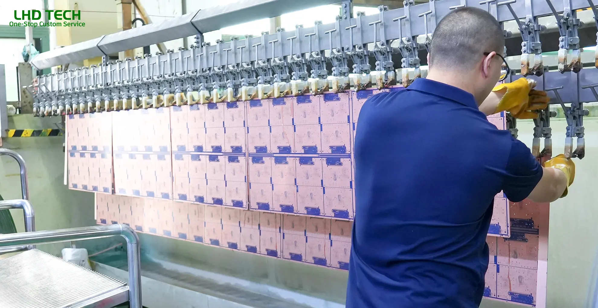
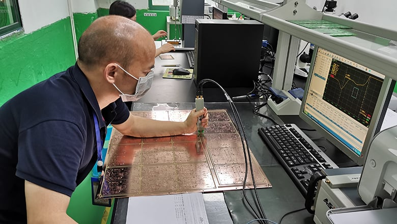
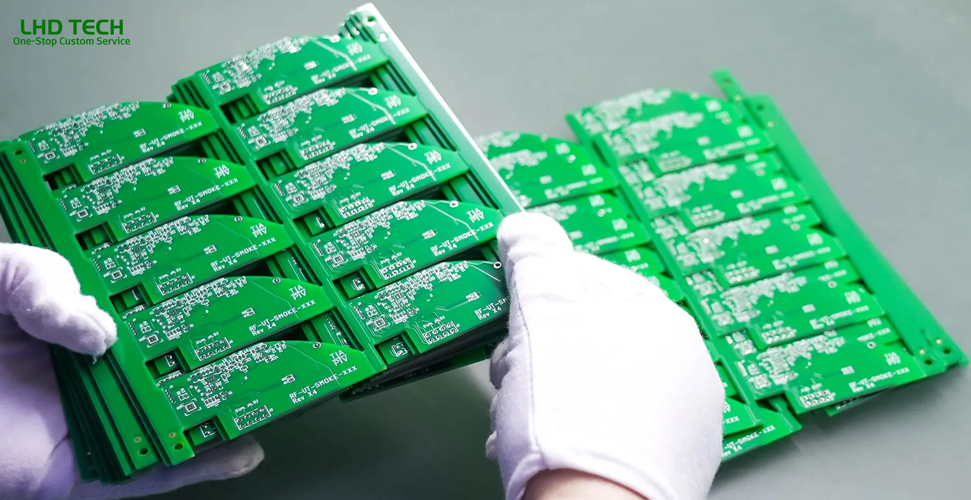
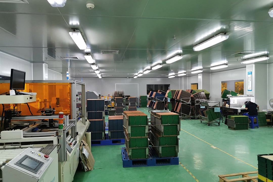
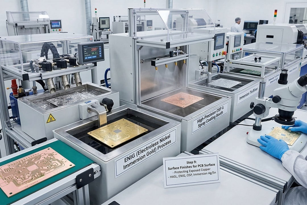
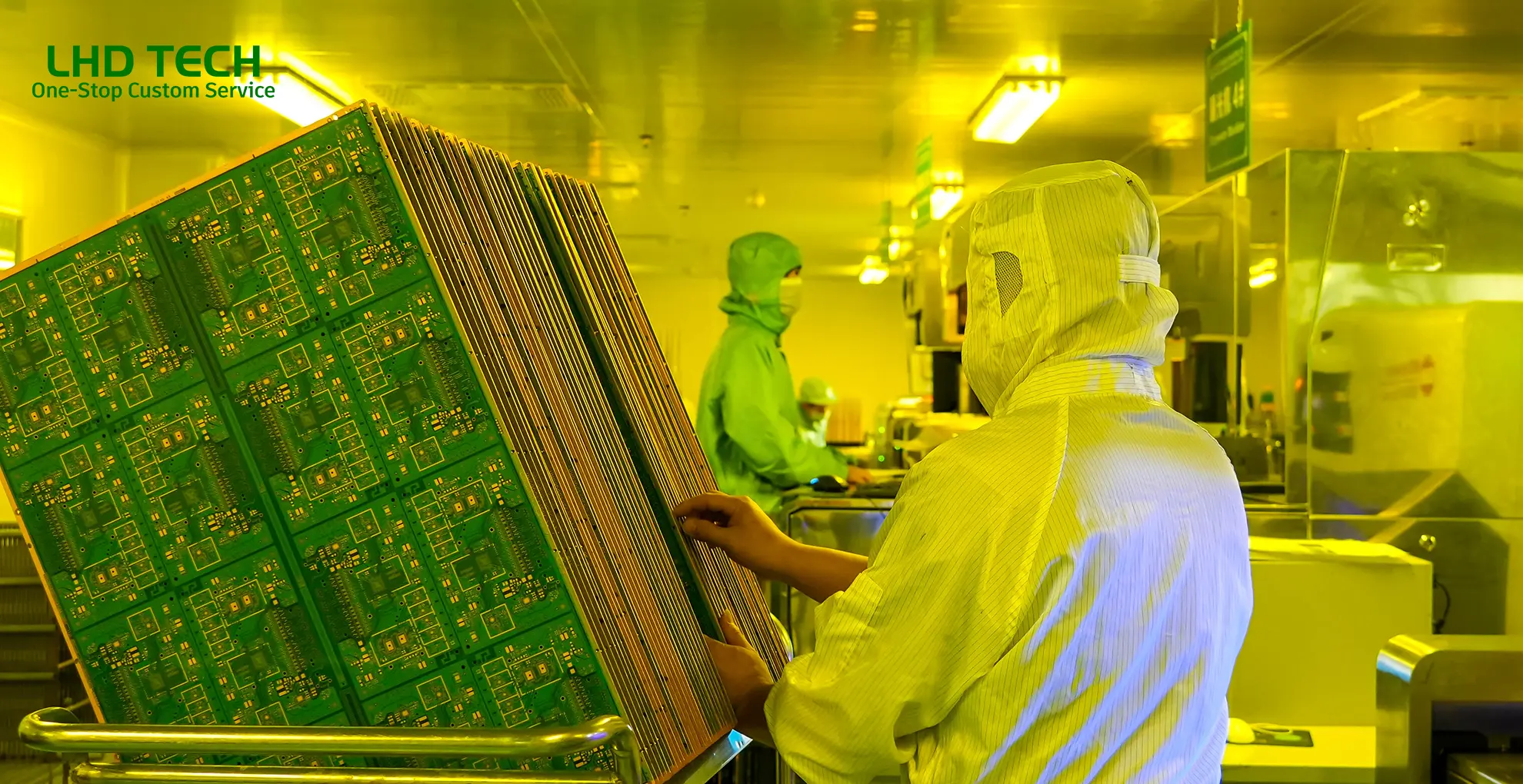
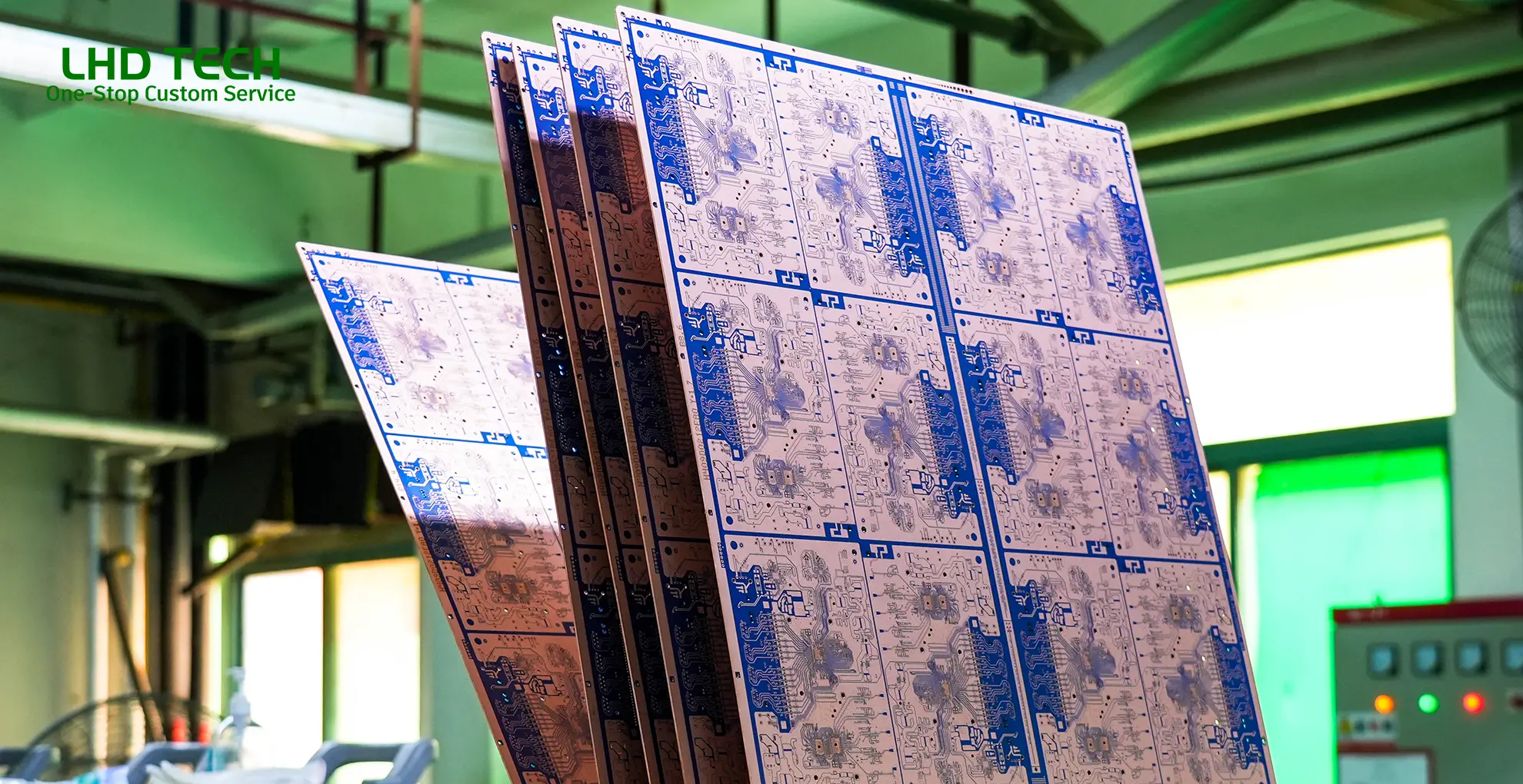
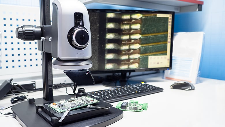
Audit-Ready Quality System
Quality & Certifications: IPC Class 2/3 Build Discipline
←
01
02
03
04
/ 04
→
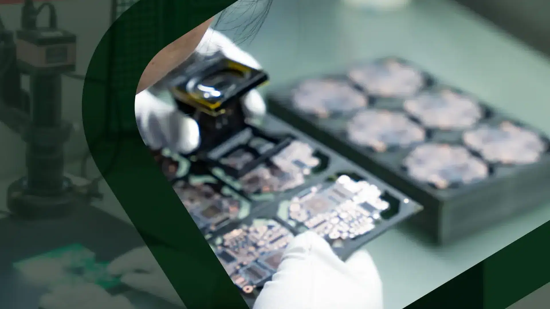
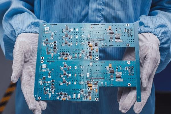
One of the first requests a quality consultant made of the engineering forums asking how to check the supplier of a PCB summarized the industry’s uncomfortable secret: An ISO framed certificate alone tells you little – and even veterans on the China EMS side concede that trusting a factory based on photos of SMT lines is one of the more frequent overseas purchasing mistakes. What those who visit factory sites really want to see are operators trained on IPC-A-610, close-out logs demonstrating actual problem solving (not an untarnished record), and proof of the traceability system’s ability to quickly retrieve a lot’s historical data.
We constructed this area as a reader views it during an inspection rather than as a salesperson pitches it – and we’d prefer to demonstrate our system than hang certificates. Certificate documents for each of the claims we make can be provided on demand, and customer-auditing for well-qualified organizations is always welcome.
Certificate Documents — Provided on Demand
08Files
Management systems
ISO 9001
Quality management
ISO 14001
Environmental management
IATF 16949
Automotive quality context
Product & material compliance
UL-recognized materials
94V-0 flammability rated laminates
RoHS / REACH
Substance compliance declarations
CE
Where product scope applies
Workmanship & acceptance standards
IPC-A-600 / IPC-6012
Bare board acceptance, Class 2 & 3
IPC-A-610
Assembly acceptance, Class 2 & 3
J-STD-001
Soldering requirements
IPC-A-610 Acceptance Delta
180°Wetting
IPC CLASS 2
270°Wetting
IPC CLASS 3
Circumferential solder wetting — one of the visible Class 2 vs Class 3 acceptance deltas
Two details separate stringent quality systems from a document collection.
01
First, the class distinction is real engineering, not a sales tactic: IPC-A-610 tightens acceptance from Class 2 to Class 3 across solder wetting, fill, and placement criteria (industry references cite 180° versus 270° circumferential wetting as one of the visible deltas), and Class 3 via plating is verified at the barrel’s thinnest point rather than as an average – plating thins toward a via’s center, which is exactly why the measurement location matters.
02
Second, the class is locked at fabrication; there’s no way to assemble a Class 2 bare board into a Class 3 product, so the acceptance class belongs on your purchase order.
Our inspection stack – AOI, x-ray, and flying probe equipment – enforces those acceptance criteria on the line, and we provide a detailed overview of the quality certifications and standards we adhere to on our Certifications Page, along with the full picture of our PCB manufacturing capabilities.
3
Buyer Advisory, Auditing Any PCB Supplier (Including Us)
Prior to awarding any program, ask any supplier for three things: the operator training matrix against IPC-A-610, one closed corrective-action report with root cause, and a live traceability pull on a historical lot. Anyone who hesitates on any of the three is telling you something a framed certificate can’t.
01
02
03
04
Would you prefer the paper first and the conversation later?
Simply request documentation of certifications→
How to Order: RFQ to Boards in 5 Steps
This story board buyers tell is all too familiar: the RFQ goes into a portal, the quote come back without any stack-up assumptions, and when the schedule slips there's no shipping notice, no delay confirmation, no reply after 5 attempts - a verbatim quote from an engineering forum that perfectly captures the exact pain our ordering process is built to solve. Siemens’ electronics design group explains why the fix must be early: approximately 80% of the final manufacturing cost is baked in during the design and development stage. Our process thus front-loads engineering review, instead of trying to race your files to the line; our Prototype-to-Production Bridge process utilizes a single engineering file set for everything from the first article to mass ramp, with no requalification or supplier switch required.
01
Upload your package
Submit your gerber file set, BOM, and centroid file through the quote form. No account, no login wall.
02
Engineering & DFM review
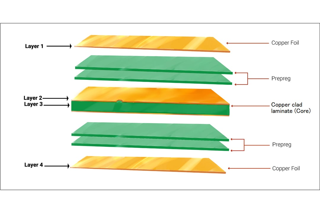
An engineer inspect for manufacturability-trace/space, annular ring, stack-up, solderability-and identifies potential issues before anything is fabricated.
03
Itemized quotation
Price of the fabrication, parts, assembly, and test on separate lines, with HTS-relevant scope disclosed to inform your landed cost calculations accurately. No-MOQ prototyping available; program-specific pricing for larger runs.
04
Build and inspect
Both fabrication and assembly performed under one quality system: solder paste inspection, first article inspection (IPC-A-610), automated and X-ray inspection (class dependent), and functional test to your specific procedures.
05
Ship and ramp
Prototype feedback is integrated into the same production recipe - the Prototype-to-Production Bridge from engineering build to volume manufacturing without starting over.
None of this is ceremony. Analyses by procurement professionals estimate that electronic components account for 60-80% of a board’s cost, with sourcing issues being a primary source of delays; that’s why BOM review happens second, not after the fabrication is placed. Front-loading engineering on our 500,000 m² annual production base makes our bridge solid: your quote becomes a fixed recipe your reorders adhere to, rather than an invitation to renegotiate. Lead times are quoted with stack-up and queue context, not as aspirational website promises-we hear from engineers that “quoted 5 days, delivered in 15” elsewhere causes more disruption than an honest schedule. We protect your IP rigorously-NDAs signed prior to file submission upon request, all production data stored on protected servers, line operators access only relevant station information, never your entire package. We build to your design exactly-fabrication specifications and laminate selections are respected, and we'll always present you with options before considering any material substitution.
Custom PCB Manufacturing FAQ
Request for Quotation
Send Your Gerber Files, Get an Engineer's Answer
Upload your board package and receive an itemized quotation with DFM findings - from a custom pcb manufacturer that answers with engineering, not a chatbot.