Get in touch with PCBark Company



Reviewed by the Shenzhen Linghangda Technology Co., Ltd. (PCBark) technical team. Updated July 2026.
A 4 layer pcb is a printed circuit board with four copper layers — two outer signal layers wrapped around two inner planes for ground and power — and that inner pair is enough to get controlled impedance, clean return paths, and lower emissions. But layer count is easy. Stackup, getting the target impedance you can actually measure, routing the return current in the same place as the signal, and understanding what adds cost are the tricky parts.
This guide takes a 4 layer pcb from stackup selection to a manufacturable, impedance-verified fabrication package.
Quick Specs, Standard 4-Layer Board
| Overall thickness | 1.57 mm (62 mil) typical; ~42 mil core + 2 × ~7 mil prepreg |
| FR-4 dielectric constant (Dk) | ~4.0 to 4.8 (grade- and frequency-dependent) |
| 50 Ω microstrip width | ~13 mil on a Dk 4.1, 7-mil-to-plane outer layer (stack-specific) |
| Impedance tolerance | ±10% standard; ±5% with tighter control + coupon |
| Copper weight | 0.5 oz or 1.0 oz/ft² outer; ½ oz inner is common |
| Radiation vs 2-layer | ~20 dB lower with solid reference planes |
Four-layer PCBs lay the signals on the outer two layers and reserve the inner two for solid reference planes, giving every trace a nearby return path for controlled impedance and low EMI. The standard 1.6mm thick build yields a 50 ohm signal on roughly a 13mil microstrip with about a 10% impedance variation.
You use one if you’ve a controlled impedance net, fast edges, fine pitch high density parts, or a margin of EMI to maintain.
Key takeaways
- Four layers are not inherently better; a well designed 4-layer board may perform better than a poorly designed 6-layer.
- Trace width from the impedance calculator is only an estimate: the actual delivered impedance will vary because FR-4 DK will differ, and thickness may only be held to 10%.
- Cost comes from lamination cycles, not the number of layers. It is blind and buried vias that make the jump, not the fourth layer.
- Number one mistake on a 4-layer board: routing a fast signal across a plane split, breaking its return path.
What a 4-layer PCB actually buys you (and when it doesn’t)

What a 4-layer board buys you is a reference plane. Its two inner layers put a solid ground plane directly beneath every signal, and that one change delivers controlled impedance, continuous return paths, and roughly 20 dB lower emissions than the same circuit on two layers — provided your layout respects it.
A 4-layer PCB is basically a 2-layer board with two buried copper layers-nearly always used for reference-and the change is a big deal. This added layer doesn’t just provide “more space” for routing; instead, it means that each signal layer is positioned immediately above a solid reference plane. This plane offers a direct, low-inductance path for the signal’s return current to follow directly below the trace, which is the basis for controlled impedance and minimized loop area.
In the usual arrangement the top layer and bottom layer carry the two signal layers, while the inner pair splits into a ground layer and a power layer separated by an insulating dielectric, keeping signal and power cleanly divided. By keeping each signal very close to a solid ground plane, a 4-layer board can be around 20 dB quieter — it radiates far less electromagnetic interference — than an equivalent circuit on 2 layers.
Here is the key physics principle — the reference plane: the trace and the solid plane below form a transmission line, where the current on the plane is a copy of the current on the trace, and it flows beneath it. On a 2-layer board, the trace has to find its return path wherever a ground trace is nearby, creating a winding path with large loop area.
Having two solid inner planes creates that ideal path under each signal layer-but only if your layout follows them. Get it wrong — route a fast trace across a plane gap — and you inherit the exact 2-layer failure you paid to escape: the return current forced into a large loop, radiating EMI and coupling into neighboring nets.
Under what conditions can you avoid the 4th layer?
If you’re working with slow signals, a low density design, or have no need for controlled impedance, two layers with a good ground plane fill will do just fine, often arriving faster and cheaper. Layer count should always follow the electrical requirements of the circuit.
Point to remember: The fourth layer provides a reference plane, not simply more space to route.
All of the subsequent work rests on ensuring you protect that plane.
The 4-Layer Stackup Crosswalk: three arrangements and how to choose
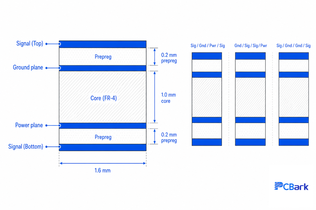
4-Layer Stackup Crosswalk – a side-by-side view of your pcb stackup options: three workable four-layer pcb stackup design choices, each mapped to the design it wins.
Your 4 layer pcb stackup choices are not one fixed thing: there are really only three arrangements worth contemplating, and choosing among them is a decision, not a default. That default stack most tools offer (Sig/GND/Power/Sig) isn’t necessarily the right one.
| Stackup (L1–L4) | What it gives you | Best for | Watch out for |
|---|---|---|---|
| Sig / GND / PWR / Sig | One ground, one power plane; simplest PDN | Mixed digital designs with a single dominant supply | A layer-1→layer-4 signal changes reference from GND to PWR |
| Sig / GND / GND / Sig | Both signal layers reference ground; power routed as pours | High-speed / SI-critical work, multiple supplies | You must hand-route power; no solid power plane |
| Sig / PWR / GND / Sig | Mirror of the standard stack | When most routing sits on the bottom layer | Same reference-transition issue as the standard stack |
What makes the two-ground stackup (Sig/GND/GND/Sig) subtle for high-speed work is this: In the standard configuration, when a signal trace changes layers between top and bottom, it changes its reference from a ground plane to a power plane. This isn’t fatal-a power plane functions as an ac ground as long as it’s well decoupled-but any such layer change requires a nearby stitching capacitor to conduct the return current across the plane gap. A two-ground plane arrangement, on the other hand, maintains ground reference on both outer layers, which results in cleaner layer transitions and allows for a plane-to-plane stitching via instead of a capacitor. Research on stack-up designs published by Missouri University of Science and Technology treats reference-plane assignment as a first-order variable, not a design detail.
“The point of four layers is to have two planes. When a signal switches layers, you want the reference to stay ground, that is what keeps the return current continuous.”
Decision Criteria: If your top priority is signal integrity, then you’ll want to go with a Sig/GND/GND/Sig stackup and handle power distribution as a pour. If a solid power plane greatly simplifies your PDN and speed is less critical, a standard stackup with strategically placed stitching caps works well.
The Impedance Tolerance Ladder: controlled impedance you can calculate yourself
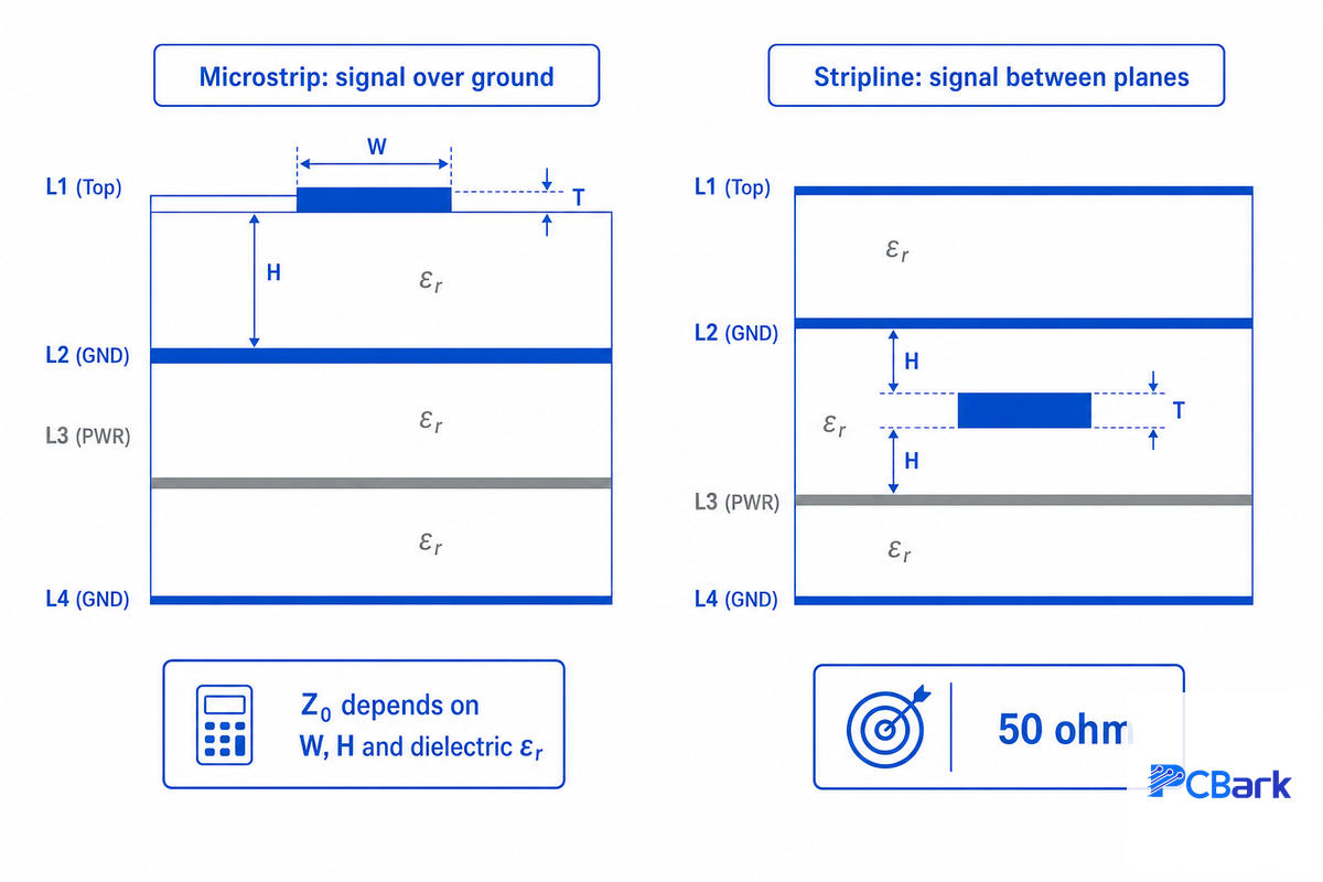
The Impedance Tolerance Ladder -the rungs between the number you get from the calculator and the board a fab ultimately produces.
Achieving controlled, consistent impedance on a 4-layer board isn’t difficult or overly expensive. You don’t necessarily need to use a field solver to start out.
To calculate trace impedance for a microstrip over a plane, you need just four inputs: trace width, copper thickness, distance to the plane, and the dielectric constant (Dk). Textbooks such as RF-PCB Lecture Notes from Harvey Mudd College simplify it down to one key ratio: width divided by distance to the plane, which you can then scale using the Dk value. Tools like the Clemson CVEL trace-impedance calculator allow you to input geometry values directly.
Working Example: 50 Ω microstrip on a standard stack
For example, let’s use a standard 4-layer build: 42 mil core and 7 mil prepreg on both sides. This means the distance to the reference plane for outer layer traces is about 7 mils, and the dielectric Dk is around 4.1. Plug those values into a microstrip calculator, and you’ll find that a 13 mil trace width yields a 50-ohm characteristic impedance.
Simply set your router’s width constraint to 13 mils, and on paper, your entire layout will have 50-ohm impedance.
Check out the ladder and keep the outer layer copper pour 2 trace widths, ~26mil away to avoid dragging the impedance down. Switch to a buried stripline (signal between 2 planes), and the same 50 Ω will require a trace of only ~4-6 mil as the trace couples to both planes instead of just one. For differential pairs, like USB or Ethernet, that aim for 90-100 Ω, the trace width will need to be carefully matched and kept at an even closer ~5mil separation.
Now, the rung the calculator misses. FR-4’s dielectric constant isn’t a single value, but varies based on glass type, resin content, and signal frequency (commonly ~4.0 to ~4.8). On top of that, the fabricator will only control the dielectric thickness to within a tolerance, not a precise value. Consequently, a controlled impedance spec is always expressed as a tolerance band (typically ±10% of the target impedance, with ±5% only under stricter process control and coupon testing). To hit this band, the fabricator will manage dielectric thickness and resin content. Indeed, the primary impedance control parameter identified in many High-Speed Design guides, such as NASA’s High-Speed PCB Design Guide, is the dielectric-thickness tolerance between layers. Add the dielectric constant spread with the thickness tolerance, and the design calculation for a “13 mil = 50 Ω” typically ends up somewhere near ±10%.
At PCBark, our own controlled-impedance testing consistently finds that dielectric constant is the most variable element. A calculated ~13mil, 50 microstrip will routinely be off-spec on the test coupon due to resin content and glass-weave variations skewing the Dk. This is why we perform TDR testing on all controlled-impedance lots, rather than blindly trusting the calculator results. As a rule of thumb, the calculator width should be treated as an initial estimate; thereafter, request your fabricator’s coupon-verified stackup and ask them to adjust the trace width according to their specific materials.
The Impedance Tolerance Ladder, bottom to top: measured coupon → the fab’s ±10% thickness tolerance → your stack’s real Dk → calculator width. Bottom rung = verified reality; top rung = the design target.
2 vs 4 vs 6 layers: a decision that sticks
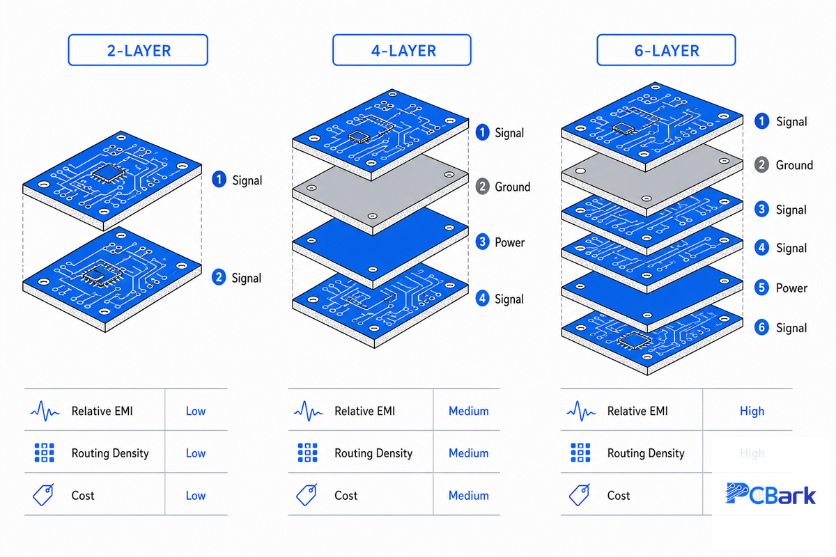
The 4 layer pcb vs 2 layer pcb question comes down to one thing: when do you know that two layers just aren’t going to cut it and that you need to move to four? And when does four suddenly not become enough? Fortunately, it’s not based on guess work but a simple checklist of trigger signals. Increment your layer count to four as soon as ANY of the following conditions are met – be honest: don’t add layers just because you can. Added layers just add to the cost and the lamination risk.
| Trigger signal in your design | Points to |
|---|---|
| Any controlled-impedance net (USB, Ethernet, DDR, RF) | 4 layers — you need a solid reference plane |
| Edge rates faster than ~1 ns / clocks above ~50 MHz | 4 layers — return-path control |
| Dense BGAs or fine-pitch parts you cannot escape on two layers | 4 layers (6+ if escape routing still fails) |
| Tight EMI margin / regulated emissions | 4 layers — plane shielding |
| Multiple high-speed buses that must cross without coupling | 6+ layers — dedicated routing layers between planes |
| High current / thermal spreading needs (motor drives, power) | Layer choice + heavier copper — not just SI |
There are two dimensions often overlooked in this decision process. First is thermal performance and current-carrying capability: a layer count driven purely by signal integrity will fail if you’re attempting to power up a stage with heavier copper, thermal vias or a plane functioning as a heatsink. The second, more contrarian dimension: more layers isn’t necessarily better. A clean 4-layer board with tight signal references often outperform a sloppy, hurried 6-layer board. More layers provide options, not correctness.
Decision rule: use 4 layers on the first controlled-impedance net or fast edge; go to six only when routing or bus isolation physically fails on four – not for reassurance.
The Return-Path Routing Tree and the 4-Layer Layout Defect Atlas
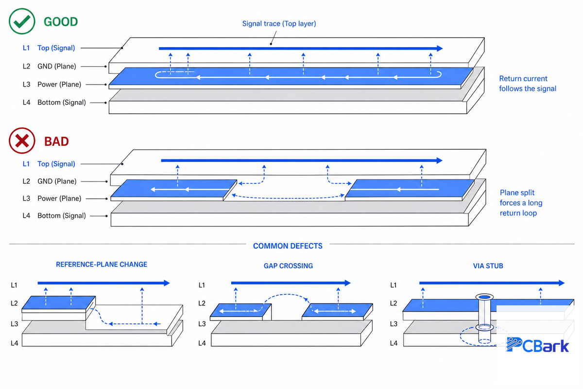
The Return-Path Routing Tree – a branch-by-branch decision for keeping every signal’s return current continuous on four layers.
Most 4-layer signal-integrity problems come back to one question: where does the return current flow? Follow this tree for every high-speed net. Is the trace over a solid, unbroken plane for its entire length? If yes, you’re done. If it crosses a gap or a split, does a stitching via or capacitor sit within a few millimetres of the crossing to carry the return current across? If the trace changes layers, does the new layer reference the same plane – and is there a return via next to the signal via? Each “no” is a branch where emissions and crosstalk increase.
The 4-Layer Layout Defect Atlas – the common layout faults, what they cause, and the solution.
| Defect | What it causes | Fix |
|---|---|---|
| Routing a fast trace over a plane split | Return current detours around the gap → large loop, radiated EMI, crosstalk | Reroute over solid copper, or bridge the split with a stitching cap at the crossing |
| Layer change with no adjacent return via | Return current has no low-impedance path across planes | Place a ground return via beside every signal via that changes reference |
| Signal layer too far from its plane | Higher, uncontrolled impedance; weaker coupling | Use a thin prepreg between the outer signal and its adjacent plane |
| Splitting the ground for “analog vs digital” | Return currents get blocked at the split → the classic mixed-signal EMI failure | Keep one unbroken ground; partition by placement, not by cutting the plane |
That last row is worth contemplating because it contradicts advice that still floats about. Cutting the ground plane to divide digital from analog sections seems deliberate, but for any signal that crosses the boundary – an analog line to an ADC, for example – the return current is required to make a lengthy detour and broadcast. Current wisdom in the signal-integrity community, reinforced by university stack-up research, is to maintain an unbroken reference plane and separate domains by component placement instead. Avoid routing high-speed signals over a split; if the plane has to be broken, treat the crossing as a controlled event with a stitching path.
Field note: on a two-ground stack you can place a plane-to-plane stitching via next to any transition via, which is why high-speed routing is easier there than on the single-ground norm stack.
Vias on a 4-layer board: types, stitching, and the cost link
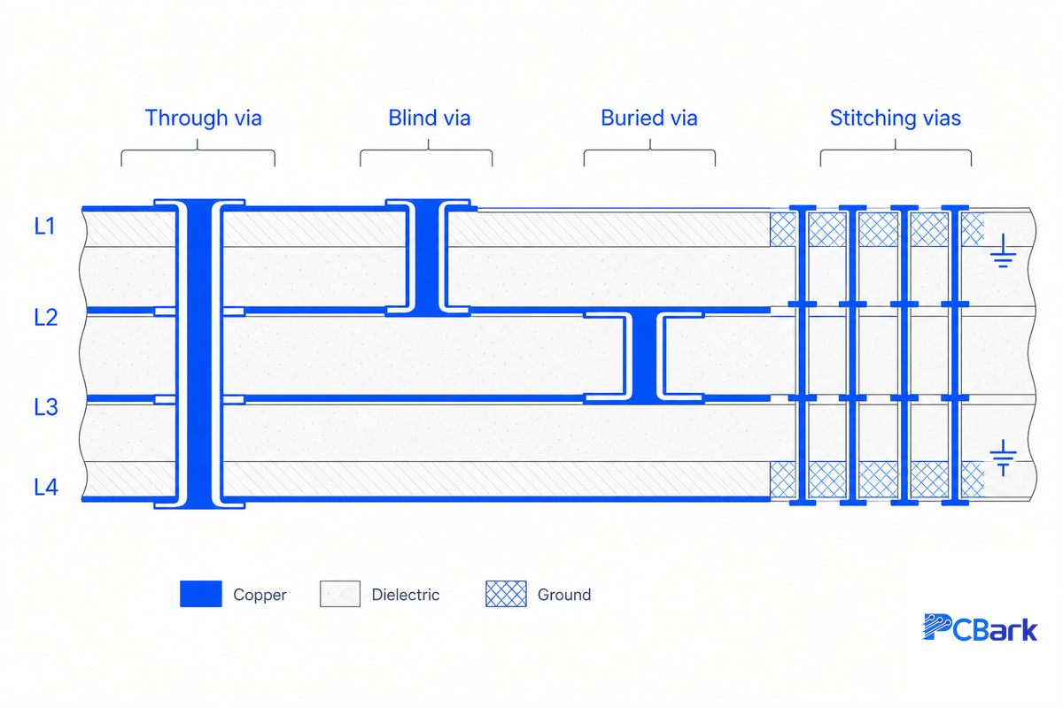
On most 4-layer boards, every via is a plated through-hole that traverses all four layers – and that’s fortunate, because a single drill-and-plate operation keeps the board affordable. You’ll employ vias for three purposes: to alter a signal’s layer, to stitch planes together — a technique called via stitching — and to convey heat or current. Blind vias and buried vias are the exception that changes the cost picture. Return vias placed beside signal vias ensure the return current remains continuous through a layer change. Stitching vias sewn around the perimeter join the two ground planes together and, on a two-ground stack, create a partial Faraday cage to contain radiation.
The 4-Layer Via Type Matrix – the nine via types a 4-layer designer selects among, and what each one costs in lamination.
| Via type | What it connects | Lamination impact | Use it when |
|---|---|---|---|
| Through-hole (plated) | All 4 layers, top to bottom | Single cycle — cheapest | Default for most 4-layer boards |
| Blind | Outer layer to one inner layer | Adds a lamination cycle | Escape routing under fine-pitch BGAs |
| Buried | Two inner layers only | Adds a lamination cycle | Freeing outer-layer routing space |
| Microvia (laser) | Adjacent layers, ~100 µm drill | HDI sequential build | HDI 4-layer, ≤6 mil features |
| Via-in-pad | Component pad to inner layer | Needs filling + capping | BGA fan-out where space is tight |
| Thermal via | Component pad to a plane | Single cycle | Spreading heat under power parts |
| Stitching via | Ground plane to ground plane | Single cycle | Faraday-cage EMI containment |
| Return via | Beside a signal via, to the plane | Single cycle | Every high-speed layer change |
| Tented / plugged | Any via, sealed per IPC-4761 | Finish step, no extra cycle | Protecting vias near or in pads |
What really drives cost, though, is the blind and buried via. A blind via only goes from an external layer to an internal one; a buried via connects two internal layers. Either necessitates an extra lamination cycle – known as sequential lamination – as the board is built and laminated more than once. It’s this second lamination that’s the real cost driver, not the fourth copper layer itself. A more typical through-hole via, on the other hand, gets drilled at the standard 10:1 aspect ratio with a ~6 mil drill bit, keeping annular rings around the pads to a minimum of ~2 mil for IPC Class 2 all in one pass. Manufacturers even tout specialized multilayer board construction techniques with patents, like US Patent 5,196,087 which combines high-controlled-impedance construction with precise stack-up and lamination control, and US Patent 7,215,007 which discusses a compact 4.5-mil power-ground plane pair optimized for interplane capacitance. For most basic 4-layer boards, just stick with through-hole vias and reach for blind/buried vias only if necessary for escape routing.
Your choice of via protection and acceptance is driven by the standards bodies, not your contract manufacturer. IPC-4761 covers the types of via protection (tenting, plugging, filling, or capping). Revision F of IPC-6012, which was released in 2023, specifies acceptance and qualification criteria for rigid boards, including criteria for annular rings and copper wrap. Acceptance classes specified in that standard (and IPC-A-600 for visual acceptance) will be the lingua franca between your team and your fabrication vendor once the board is entering pcb production.
Key point: The cost of layer count is inexpensive. Additional lamination cycles, on the other hand, are costly. Try not to reach for blind and buried vias as your first choice.
Power integrity: making the plane pair work for you
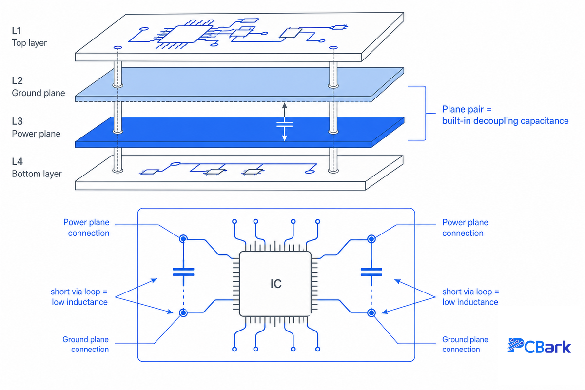
On a 4-layer board you get one solid ground plane and one power plane. Paired across a thin insulating dielectric, this ground and power plane forms a parallel plate capacitor (interplane capacitance) — the same compact power-ground plane pair described in US Patent 7,215,007 — and that structure gives you an excellent distributed decoupling solution right where high-speed ICs and their power supply demand current. Unfortunately, spacing limits how much interplane capacitance you can practically achieve. In a typical 0.062-inch 4-layer stack, the power and ground planes are often 0.020 inch or more apart, limiting capacitance. Above about 200-300 MHz, your typical surface-mount decoupling caps start to become ineffective as they behave more like inductors, and widely spaced power/ground planes simply can’t compensate for them.
As a result, be mindful of your plane-pair design. Place your decoupling capacitors as close to the IC power pins and the power rail as possible to minimize loop inductance, and for a 4-layer board, consider tying the cap to the pin that connects to the outer plane to keep the current loop tighter. Beyond a few hundred MHz, a standard 4-layer stack will quickly become insufficient to support your power distribution network (PDN). Either specify tighter plane spacing (non-standard) or plan on moving to a 6-layer board with dedicated inner power/ground planes. One word of caution from the modeling literature, though: don’t think that just pairing up power and ground planes with some dielectric in between automatically eliminates the PDN design challenge. Academic analyses, such as this arXiv paper on plane-pair cavities, show that resonant peaks can develop in the plane cavity, causing interference to radiate throughout the board, so careful placement of your decoupling caps and cutouts is still important, even with the enhanced capacitance.
Key point: The plane pair is your fastest decoupling component and your potential resonator. Thin spacing, careful cap placement – those will determine which it becomes.
What really drives 4-layer cost (the levers you control)

What drives 4-layer cost is lamination cycles, not the copper-layer count. A standard single-lamination 4-layer board sits close to two-layer pricing; the real jump comes when blind or buried vias force sequential lamination. Tolerance, copper weight, and finish move the number after that.
As a designer, you’ve much more control over 4 layer pcb price than the quote implies – but not by counting layers.
A four-layer board does cost more than a two-layer one, for sure: add the inner-layer imaging and inspection, the lamination cycle, extra drilling and plating. It’s not uncommon to see manufacturer cost breakdowns showing each extra copper layer adding on the order of 10-20% over a basic two-layer, or to find quotes that place a two-layer board about 20-40% cheaper than a 4-layer. These are approximations-real costs vary a great deal depending on the manufacturer, volume, finish, and copper weight.
What’s remarkably stable is the order of the cost levers.
| Design lever | Cost impact |
|---|---|
| Blind / buried vias (sequential lamination) | Largest — each extra lamination cycle is a step change |
| Tighter impedance tolerance (±5% + coupon) | Moderate — added test and material control |
| Heavier copper (≥2 oz), exotic laminate | Moderate — material and process |
| The fourth layer itself (single lamination) | Smallest of the four — closer to 2-layer than to a blind/buried build |
That shifts the cost conversation. A four-layer board, in a single-cycle design-that’s the version with standard through-hole vias, standard tolerances, standard copper weight-is cost wise only a modest step up from two-layer, not a true blind/buried multilayer build.
But add a single blind or buried via and the whole board must go through an extra lamination step — the sequential lamination controlled in processes like US Patent 5,196,087 — and the price takes a jump. (A well-designed four-layer board, remember, will actually lower the total project cost by saving you the respins and EMI debugging cycles you’d never see on the fabrication quote.) So don’t throw lamination cycles in every where; reserve them for where you absolutely must.
Key point: The cost ranking is Blind/Buried Vias > Tolerance > Materials > The Fourth Layer. Design around lamination cycles, not layer count.
The 5-Stage Stackup Setup Workflow: from EDA tool to fabrication package
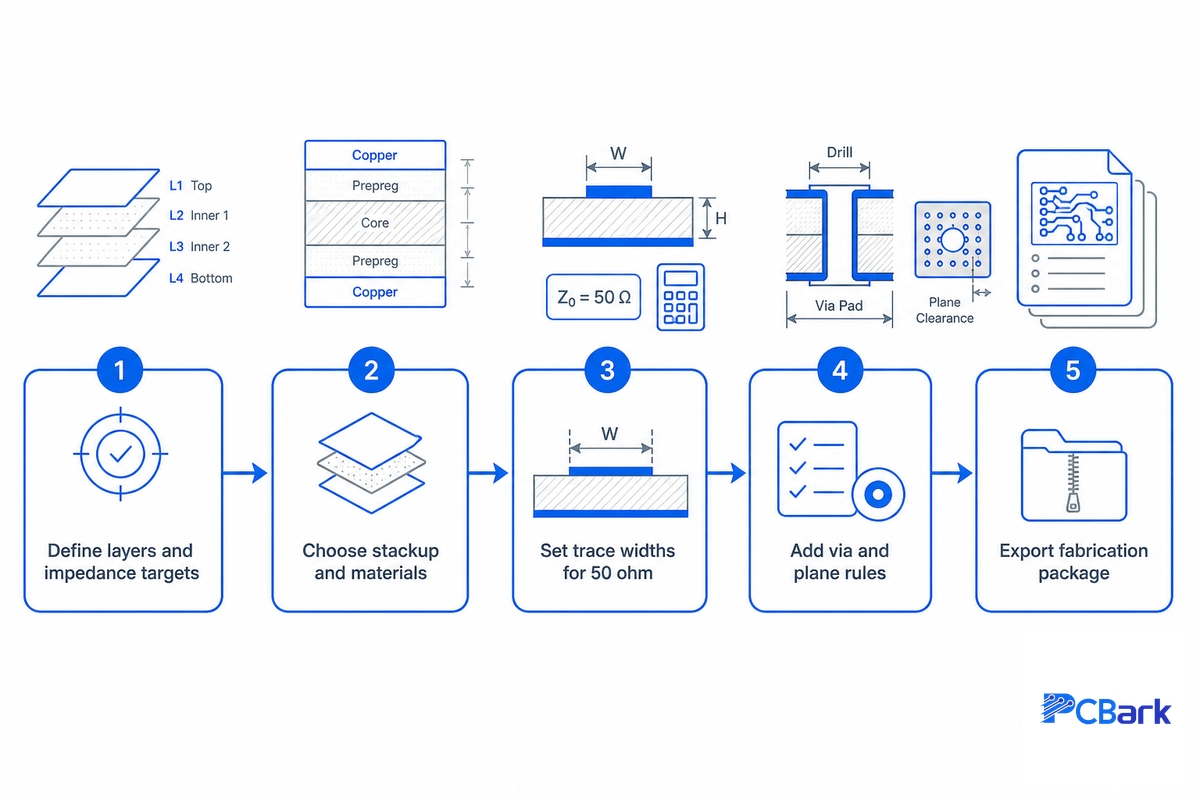
The 5-Stage Stackup Setup Workflow – tool-independent sequence for getting a computed 4-layer design to a manufacturable order.
No matter if you use KiCad, Altium or EasyEDA, the best practices for a 4 layer pcb design in modern electronic design are the same. The first four steps are all taken within the design tool; step 5-which too many tutorials neglect-is what takes your design from theory to an order that a manufacturer can successfully process.
- Step 1: Define the stackup in your editor’s Layer-Stack Manager, assigning your top and bottom layers to signal, middle two to ground and power, setting your total desired board thickness (most likely 1.57 mm) and configuring core/prepreg thickness to get each signal layer close to the associated ground plane.
- Step 2: Input the impedance profile. Set your Dk, width, and thickness so the tool calculates trace impedance (e.g. 50 ohms for single ended traces) and use that to assign Net Classes to appropriate traces.
- Step 3: Assign nets to layer and plane layers. Typically you assign your controlled impedance signals to the plane layer they’re referenced to; if you’ve two ground planes you can separate your power planes to have one reference the one closest to it.
- Step 4: Set up your Design Rule Check (DRC).
Specify all impedance width constraints and other relevant clearances (typically a 2x trace width for pour to trace) and checks (like crossing splits) to make the design tool catch routing mistakes.
- Step 5: Export your fabricator files. This is the make-or-break handoff.
You want to export a full stackup drawing with the impedance specified, the drill file with layer mapping and polarities, a note regarding copper balance, and a request for an impedance test coupon. That’s how you ensure that the shop applies their own CAM adjustments to match your design and achieve its controlled impedance – rather than just relying on the raw Gerber data.
Key point: this fifth stage is where a 4-layer stackup flies or dies. An ideal stackup in the editor means nothing if it ships without a controlled-impedance callout and coupon request — the fab is left guessing, and you’ll receive boards that meet your Gerber net list but not your target impedance.
Specifying the stackup, callout, and coupon are the elements that enable the four-layer design to be produced, not just to appear on the screen. Tools like the MIT microstrip calculator are valuable as an initial check on any width specifications your EDA tools suggest in the stackup profile.
Important concept: the fabrication package – the stackup drawing, impedance callout, drill table, and coupons – is the fifth stage of the process and is the stage where your modeled impedance meets reality of the fab line.
The 4-layer board in a high-speed and HDI era

4-layer design is getting tougher not because the boards have changed, but because the speeds of interfaces keep accelerating. 5G radios, AI server fabrics, DDR5 at 6400 MT/s and PCIe 6.0 at 64 GT/s have driven interface edge rates that would once only have been found on backbone gear down onto general product boards. Each interface represents a controlled impedance net requiring a return path — the discipline captured in NASA’s High-Speed PCB Design Guide – the exact recipe that takes an interface that might have once been implemented on 2 layers up to 4. That correctness bar has been ratcheted up even though the package format has not evolved.
You’ll want to watch two industry developments. First, HDI and ultra-HDI technology processes currently bring the traces and spaces down to about 25 µm, giving you the routing density to fit escape routing that would have pushed the layout to six or eight layers on prior tech; that design flexibility means a well-made four-layer HDI board now serves a wider variety of designs than before. Second, current acceptance criteria apply: IPC-6012 Revision F (2023) and IPC-2221C (2023) are the current reference specs for rigid and generic design respectively and they tightened the cavity rules, the copper-wrap, and the dielectric thickness constraints that apply to a high-reliability four-layer layout.
For some context, market reports say the high-speed and HDI portions of the pcb industry are growing faster than the total PCB market, mainly driven by demand for AI servers and automotive electronics, though this provides direction, not specifics, it reinforces what physics indicates.
Outlook: The four-layer board is the workhorse “sweet spot” but increasing interface speeds will make reference plane control and a proven stackup all the more critical for getting a design to work rather than just passing EMI.
FAQ: frequently asked 4-layer PCB questions
What is the standard 4-layer PCB stackup?
View answer
A typical 4 layer stackup is Signal / Ground / Power / Signal on a 1.57mm (62 mil) board. A thick core lies between the two inner layers, and there’s thin pre-pregs between the top and bottom layers and their nearest planes. If you’re doing a lot of high speed design, then you’ll likely want a Signal / Ground / Ground / Signal stack and pour all your power as copper, so all your signals have a ground reference and all layer changes are ground referenced.
These are both normal designs. Pick the one whose top priority is signal integrity versus a good power plane.
How do you get 50 ohm impedance on a 4-layer board?
View answer
Set trace width according to your stack-up. For a standard 7 mil to outer-copper, Dk ~ 4.1 pre-preg build, a 50ohm trace will be around 13 mils, and a buried stripline would need to be even thinner. Plug in your Dk and geometry to an impedance calculator or your EDA tool’s impedance profile, leave two trace widths between neighboring copper pour, and know that the shipped board can typically maintain a 10% impedance control due to Dk variation and fab tolerance. Ask for a test coupon to be sure.
Is a 4-layer PCB much more expensive than a 2-layer board?
View answer
Cost is higher, but not due to the 4th layer. For single-lam 4-layer with through-holes, the economics is much closer to a 2-layer. We estimate a 2-layer at 20-40% less costly. Blind and buried vias driving additional lamination cycles add significant expense. However, the 4-layer with its ability to route complex designs, reduce respins, and manage EMI could end up cheaper for the project.
When should I use a 4-layer PCB instead of 2 layers?
View answer
Step up to four layers when you’ve the first controlled impedance net, fast edge rate signals (<1ns), a high pin count BGA that won’t escape on 2 layers, or very tight EMI margin. For slow, simple designs, a 2-layer board with solid ground pour is usually adequate.
Is a 3-layer PCB possible?
View answer
Not usually. PCBs are normally manufactured with symmetrical lamination pairs (a top and bottom layer are processed together) – 2, 4, 6, 8, etc. A design that “needs three layers” would be built as a 4-layer board, with one layer remaining mostly unused.
Building a 4-layer design?
Provide your stack-up details and impedance targets to a fabricator that TDR-verifies controlled impedance lots. Our PCBark 4-layer PCB manufacturing service includes coupon verification of your stack-up, or view the full range of multilayer PCB stackups up to 40+ layers.
Unsure about which stack-up or layer count to choose? Ask for a complimentary DFM review before committing to the final layout.
This page includes specific stack-up values and tolerances based on common engineering practices and specific fabrication capabilities. Our Dk-4.1 example is a generalized illustration, and actual values will vary with your chosen PCB materials. Our cost observations and Dk-variation remarks are drawn from real controlled-impedance manufacturing experience.
References & sources
- High-Speed PCB Design Guide – NASA Small Spacecraft Systems Virtual Institute (impedance-control tolerance).
- Design Tricks for RF PCBs, Lecture 25 – Harvey Mudd College (microstrip impedance).
- Using Transmission Lines, Chapter 21 – Oregon State University (characteristic impedance in FR-4).
- Machine-Learning-Based PCB/Package Stack-up Optimization for Signal Integrity – Missouri University of Science and Technology.
- PCB Trace Impedance Calculator – Clemson University Vehicular Electronics Laboratory (CVEL).
- Microstrip Analysis/Synthesis Calculator – Massachusetts Institute of Technology (gEDA mcalc).
- Analysis of Power/Ground Plane Configurations in PCBs – arXiv (plane-pair resonance).
- US Patent 5,196,087 – Method for making multi-layer printed circuit board (controlled impedance via lamination control).
- US Patent 7,215,007 – Suppression of electromagnetic coupling (low-profile power-ground stack, interplane capacitance).
- IPC IPC-6012F (qualification of rigid board) IPC-4761 (via protection) IPC-2221C (general design) IPC-A-600 (acceptance)