Get in touch with PCBark Company

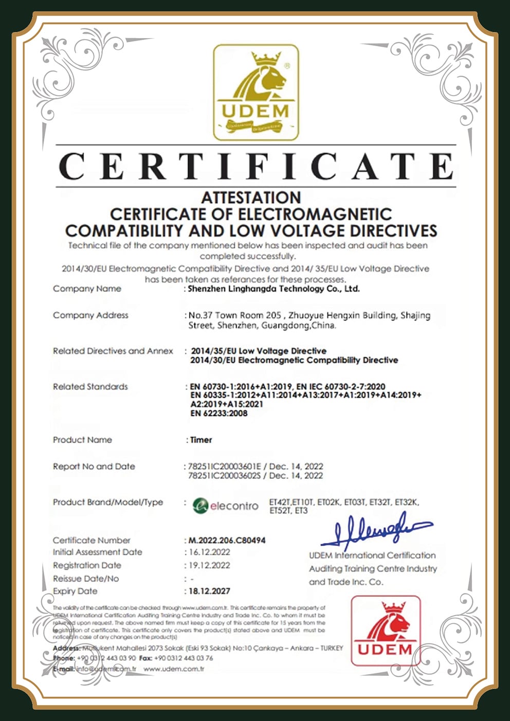
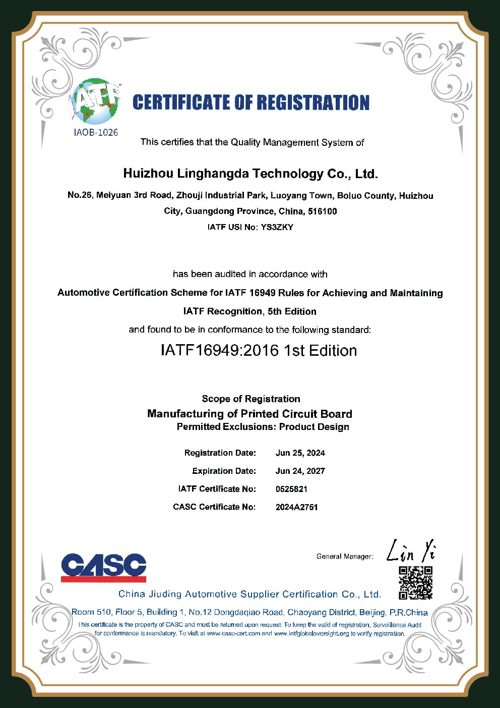
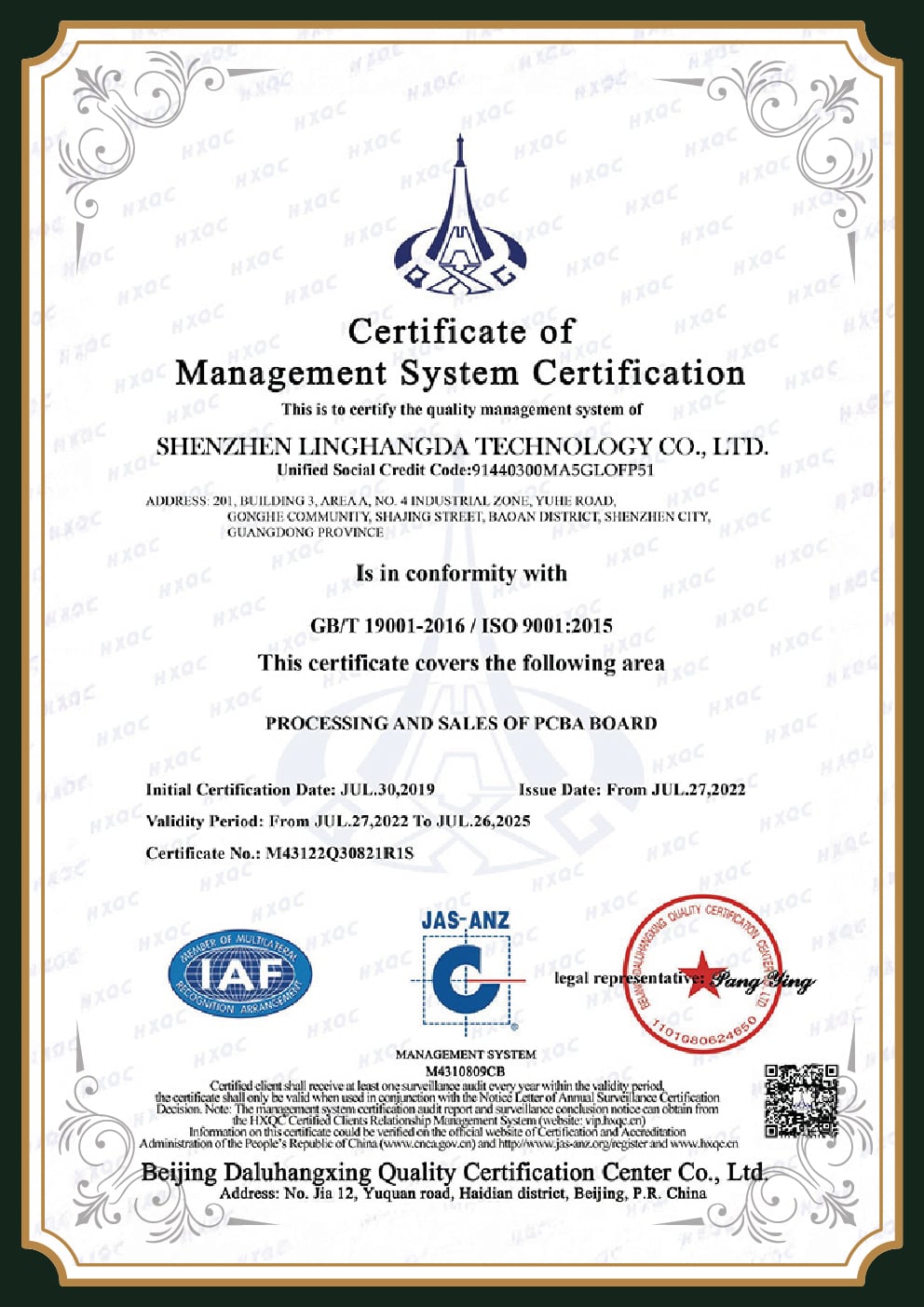
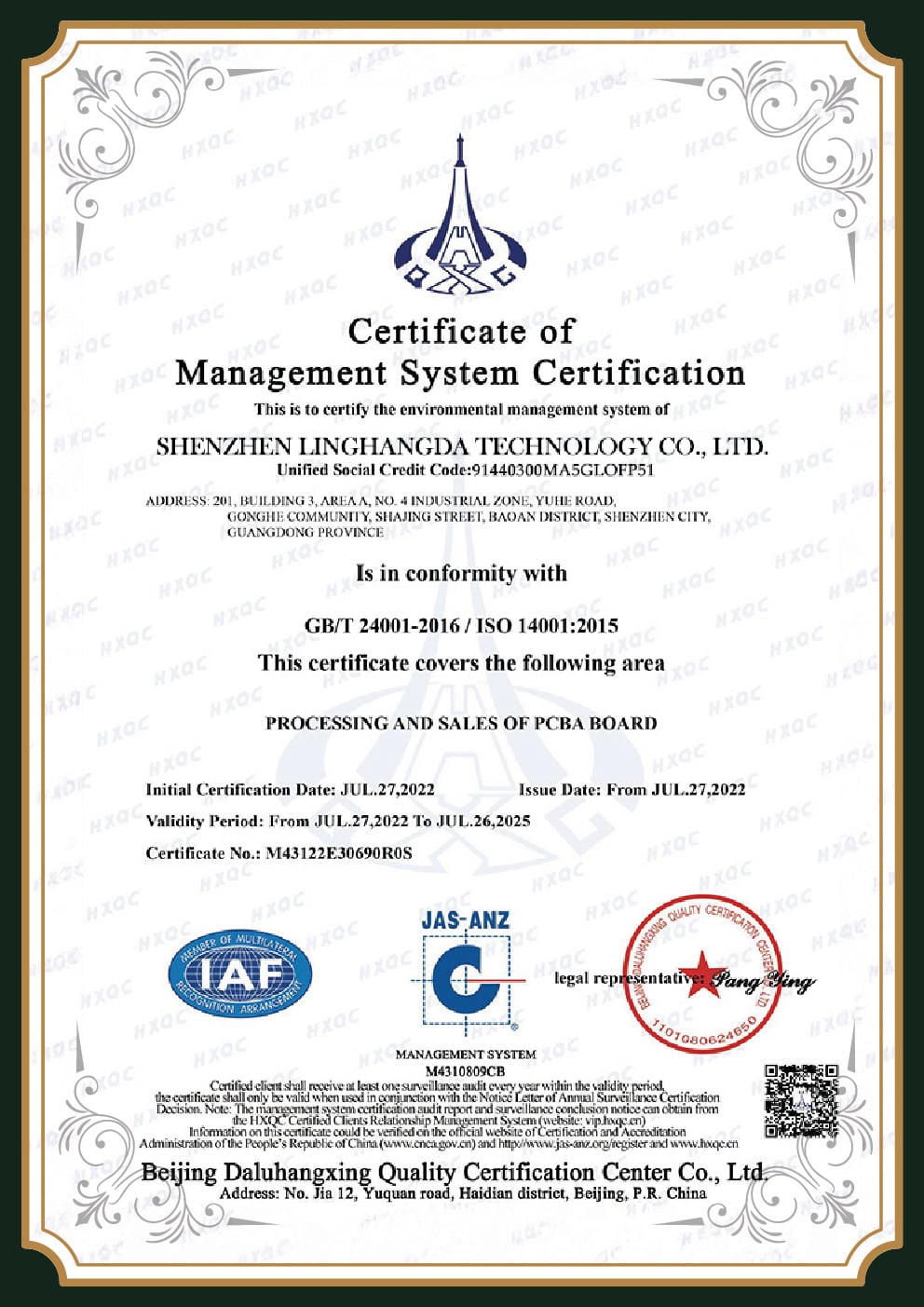
ISO Certified
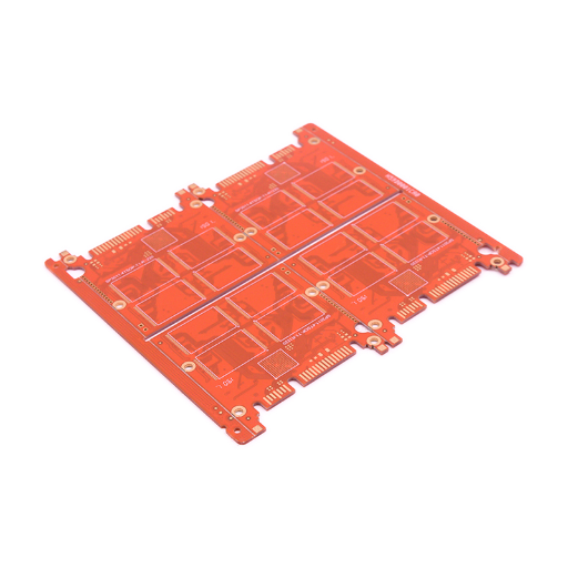
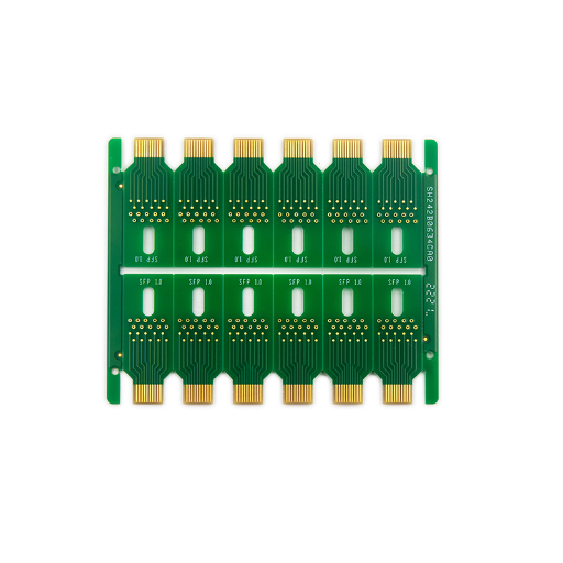
Gold Finger PCB (Edge Connector)
Gold Finger PCB Manufacturer, Hard Gold Edge Connectors Built to IPC
Hard gold fingers that survive the insertion count your product actually needs, speced to your application, not over-plated to inflate the invoice.
- ±5% Impedance control
- IPC Cls 2/3 Acceptance + 100% E-test
2–32
Layers
15–50+ µin
Hard gold thickness
500–5,000+
Insertion cycles
20°/30°/45°
Bevel angles
Why Gold Finger Wear Decides Your Board’s Field Life
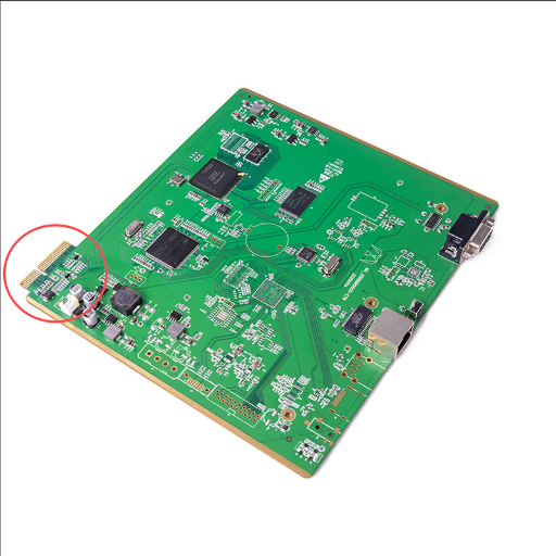
A gold finger PCB carries gold-plated contact pads along the board edge that plug straight into a card-edge socket, the same interface you see on a memory module or a PCIe edge connector. Those pads, also called edge fingers, take the full mechanical stress every time the board is inserted and pulled. You’ll find the same gold fingers on a graphics card sliding into a motherboard slot, where gold’s conductivity keeps the signal clean across every reconnection. When the plating wears through to the nickel barrier, contact resistance climbs, signals drop out, and the board fail in the field, often after it has already shipped to your customer.
What Are Gold Fingers On A PCB?
Gold fingers are hard-gold-plated copper pads at the edge of a printed circuit board that form a repeatable plug-in contact with a mating card-edge slot. The gold sit over a nickel barrier and is alloyed with a trace of cobalt for hardness, so the contact survives hundreds to thousands of insertion cycles without the contact resistance drifting.
Industry Insight
Here’s the part most vendors won’t tell you: more gold isn’t always better. A board’s right gold finger spec comes down to one number, how many times the board get mated over its service life. A board that’s fitted once at assembly and never touched again doesn’t need 50 microinches of hard gold; an industry guide on when gold fingers are actually needed makes the same point. Over-speccing thickness, or plating the whole board instead of just the fingers, adds 15–30% to board cost with zero added reliability. Honestly, the right spec is often the thinner one. The reason PCBark engineers lead with this is simple: we match the finish to the duty cycle because over-plating only inflates your invoice, then build it to a standard you can audit. Unlike a vendor paid by the microinch, we’ve no reason to upsell gold your board will never wear, and that trade-off is the difference between a quote that look cheap and a board that stays cheap once it’s in service.
PCBark Gold Finger PCB Capabilities — Standard, High-Wear & HDI Tiers
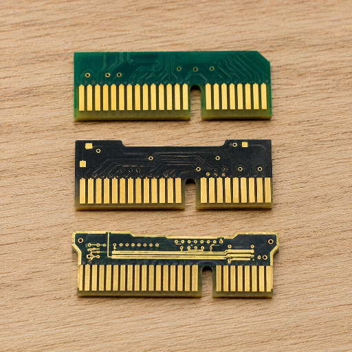
Engineers waste days trying to reconcile a vendor’s vague “1–30 layers, various thicknesses” against a real design. So here’s the full build envelope as three concrete tiers, the 3-Tier Gold Finger Capability Matrix. Find the row that matches your duty cycle and board complexity, and the column tell you the exact spec we run in production. Every value below is what PCBark’s Shenzhen line holds today, not a marketing ceiling. Unlike a datasheet that lists a single best-case number, this matrix is the reason an engineer can spec a real board in one pass instead of three quote rounds.
| Parameter | Standard (memory / control cards) |
High-Wear / High-Speed (PCIe, comms) |
High-Layer / HDI (servers, AI hardware) |
|---|---|---|---|
| Layer count | 2–8 | 4–16 | up to 32 |
| Base material | FR-4 | High-Tg FR-4, Rogers, Polyimide | High-frequency / hybrid stacks |
| Board thickness | 1.0–2.0 mm | 0.6–3.2 mm | 0.4–5.0 mm |
| Copper weight | 1–2 oz | 1–4 oz | 6 oz |
| Gold finger plating | Hard gold | Selective hard gold | High-durability hard gold |
| Gold thickness | 15–30 µin | 30–50 µin | 50 µin or above |
| Nickel thickness | 100–150 µin | 120–200 µin | 200 µin or above |
| Parameter | Standard (memory / control cards) |
High-Wear / High-Speed (PCIe, comms) |
High-Layer / HDI (servers, AI hardware) |
|---|---|---|---|
| Insertion durability | 500–1,000 cycles | 1,000–3,000 cycles | 5,000 cycles or above |
| Gold finger pitch | 0.50 mm | 0.40 mm | 0.30 mm |
| Min trace / space | 0.10 / 0.10 mm | 0.075 / 0.075 mm | 0.050 / 0.050 mm |
| Beveling | 20° / 30° / 45° | 30° / 45° precision | Custom angle |
| Bevel depth | 0.3–0.8 mm | 0.5–1.2 mm | Project-based |
| Impedance control | ±10% | ±8% | ±5% |
| Max board size | 400 × 500 mm | 500 × 600 mm | 600 × 1200 mm |
| Testing | 100% electrical test | Flying probe + impedance | AOI + E-test + impedance + reliability |
Decision Matrix — match your application to a tier
| Your application | Mating frequency | Recommended tier | Gold spec |
|---|---|---|---|
| Memory module, expansion / control card | Low–moderate | Standard | 15–30 µin hard gold |
| PCIe card, industrial plug-in, comms device | Frequent | High-Wear | 30–50 µin selective |
| Server, AI accelerator, hot-swap backplane | Very high / hot-swap | High-Layer / HDI | 50 µin+ over 200 µin Ni |
| Solder-only edge, one-time fit | Single insertion | ENIG (no hard gold) | <5 µin immersion gold |
Hard Gold vs ENIG vs Selective Plating — Spec the Right Finish
Picking the wrong finish is the most expensive mistake in a gold finger order, and it runs both ways. Engineers on r/PCB regularly get caught out when they assume ENIG covers their edge connector, then watch the contact wear through; others pay for full-board hard gold when only the fingers needed it. The fix is to read three numbers off your own design, insertion count, whether the pads also get soldered, and how much edge area is involved, and let those choose the finish. The Gold Finger Finish Selector below does exactly that.
| Property | Hard gold (electroplated) | ENIG / immersion gold | Selective hard gold |
|---|---|---|---|
| Gold thickness | 15–50 µin | <5 µin (2–5 µin) | 30–50 µin (fingers only) |
| Hardness (Knoop) | 130–200 HK | 60–90 HK | 130–200 HK |
| Insertion cycles | 500–5,000+ | Limited (solder-grade) | High, in plated zone |
| Wear resistance | Excellent | Poor | Excellent |
| Solderability | Not recommended | Excellent | Mixed: ENIG elsewhere |
| Relative cost | High | Low | Medium |
| Best for | Repeated-mate edge fingers | SMT pads, BGA, one-time fit | Cost-sensitive edge contacts |
Insertion Durability Ladder
This is the single chart to keep next to your stack-up. The Insertion Durability Ladder binds expected mating cycles to the gold thickness that delivers them, so you never pay for a cycle count you won’t use:
| Expected mating cycles | Gold thickness | Nickel under-plate | Typical use |
|---|---|---|---|
| One-time / solder fit | <5 µin (ENIG) | 3–6 µm | Soldered edges, fixed cards |
| 500–1,000 | 15–30 µin | 100–150 µin | Memory, control cards |
| 1,000–3,000 | 30–50 µin | 120–200 µin | PCIe, industrial plug-ins |
| 5,000+ | 50 µin or above | 200 µin or above | Hot-swap servers, test fixtures |
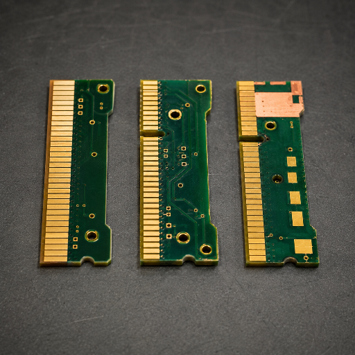
Those values come straight from published plating specifications and our own line data, not estimates. Hard gold earns its hardness from a cobalt alloy that lifts it to 130–200 HK against the 60–90 HK of soft ENIG, that hardness is the entire reason it survives repeated mating. ENIG is the better choice when the edge get soldered or only fitted once, because hard gold solders poorly. For most real designs the winning answer is the middle column: selective gold plating, selective hard gold on the fingers, a solderable finish everywhere else. It comes down to cost: gold is expensive, so PCBark plates only the contacts that actually mate. A memory module needs hard gold only on its edge contacts, so we plate only there and the rest of the board run ENIG or OSP. Unlike a full-board gold quote, this is the honest version of the spec, you pay for wear resistance only where the board see wear.
On the manufacturing floor the gold plating sequence is fixed: the copper is cleaned, a nickel barrier is electroplated, then the hard gold build over it, and only after that does the chamfer get machined and the final surface finish go onto the rest of the circuit board. Because electroplating needs current to reach the pads, the gold plating has to happen before the solder mask is cured, get that order wrong and the fingers come out patchy. Done right, that sequence is what gives an edge finger its wear resistance and the stable conductivity to survive thousands of mating cycles where a soft surface finish would erode in months.
“We get asked for 50-microinch hard gold on boards that mate twice in their life. We push back every time, we would rather quote you the 20-microinch spec your duty cycle calls for and keep your unit cost down than plate gold you will never wear. A finish that outlives the product is just buried money.”
15–30%
of board cost is what hard gold adds — so plating only the fingers (selective) instead of the full board is the largest single lever on a gold finger PCB’s price.
Source: published hard-gold plating cost data, application-dependent (PCBsync, 2025). TCO estimate — request a quote for your exact board.
Quality & Compliance — IPC-A-610 Class 2/3, ISO 9001 & 100% Testing
Behind every new-supplier decision sits one fear: the field failure that turns into a recall. Buyers comparing the big quick-turn fabs openly flag quality issues on the cheapest lines which is exactly why a gold finger board needs to be built and verified against named standards, not a vendor’s word. The reason matters: unlike a quote that simply promises “high quality,” PCBark holds gold finger work to a documented acceptance framework and inspects every panel against it, so the claim is auditable rather than verbal.
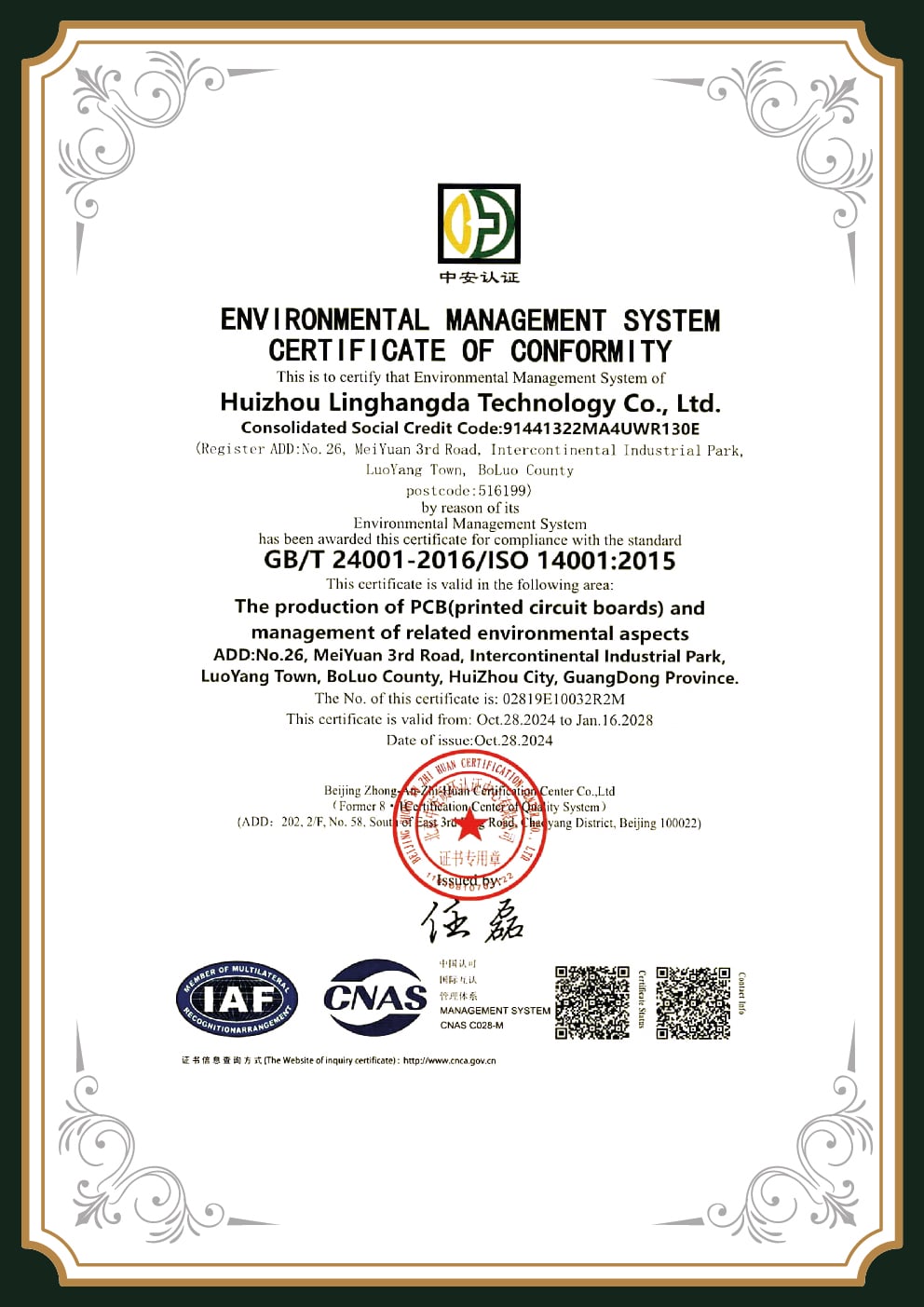
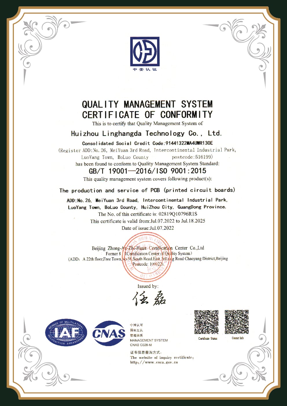
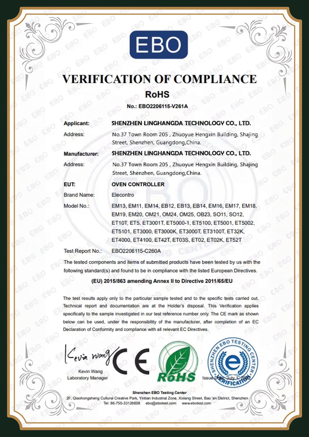
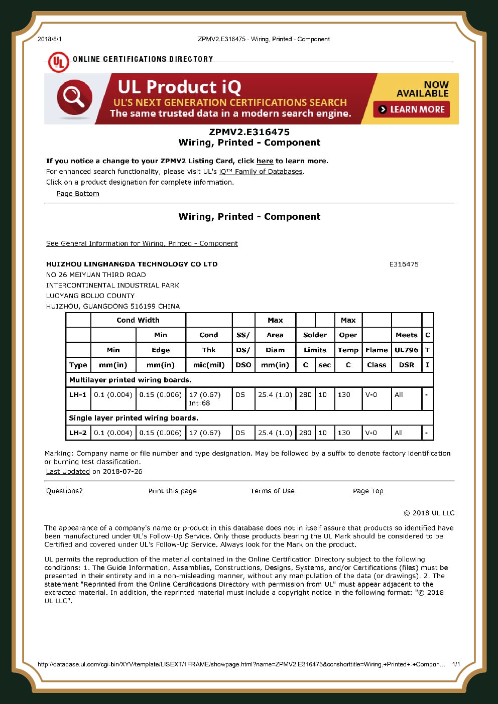
IPC-6012F
Rigid board qualification & performanceIPC-A-600
Visual acceptability incl. edge-contact platingIPC-A-610 Cls 2/3
Assembly acceptanceISO 9001
Quality management systemUL
Safety listingRoHS
Lead-free compliantThose standards split the work the way the industry intends it: IPC, accredited by ANSI, defines IPC-6012, part of the IPC-6010 series, as the performance specification (what the gold plating and structure must achieve) while IPC-A-600 is the visual acceptance guide used at inspection. For gold finger thickness the class boundary is concrete: Class 2 commercial work accepts a minimum around 25 µin of gold, while Class 3 high-reliability work requires 50 µin or more over a thicker nickel barrier. We quote and build to the class your end market demands, and we tell you which one your application actually needs.
Verification is where claims become evidence.
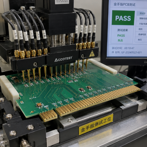
Every gold finger order passes 100% electrical test; high-wear and HDI tiers add flying-probe, impedance and reliability testing. Plating itself is checked by X-ray fluorescence for gold and nickel thickness, and adhesion is confirmed with the tape test defined in ASTM-aligned methods (IPC-TM-650 2.4.1, ASTM B571 for adhesion and ASTM B488 for the gold deposit). AOI and X-ray inspection run inline through manufacturing, so a thin or uneven gold layer is caught on our floor, not in your customer’s product.
×
![Certificate Detail]()
From Quick-Turn Prototype To High-Volume — Lead Time, MOQ & DFM Workflow
What really drives engineers offshore is consistent: they want a transparent quote, a fast turn, and assembly under one roof without paying US-shop prices. The catch they’ve been burned by is the hidden-cost quote: a low headline number that grows once rework, re-spins and miscommunication are added in. As a turnkey EMS partner with 16 years of build history, our answer is to make the cost drivers visible up front and to keep fabrication, DFM, SMT assembly and test on one line so nothing falls between vendors.
A gold finger quote moves on six levers. Knowing them lets you design to a budget instead of reacting to a number:
Ready to price your board? — itemized, with lead-time options.
Request Quote →
01 // Gold Thickness
Every extra 10 µin adds gold cost; spec to insertion count, not habit.
02 // Plated Area
Selective fingers vs full-board hard gold is the biggest single swing.
03 // Layer Count & Material
FR-4 vs high-Tg / Rogers, and 2 vs 16+ layers.
04 // Bevel & Finger Pitch
Custom angles and fine 0.30 mm pitch add process steps.
05 // Nickel Barrier Thickness
Higher reliability classes require more.
06 // Volume & Turn Time
Quick-turn prototype vs scheduled production run.
Gold Finger PCB Pricing-Factors Framework
We map your board against these and return an itemized quotation, no single opaque figure.
Quick-turn doesn’t mean a quality trade-off on the plating. That gold finger process sequence, nickel strike, hard gold electroplate, bevel, then surface finish, is fixed regardless of schedule; what compresses on a fast turn is queue time, not plating control.
Component sourcing for turnkey builds runs through authorized distributors with traceability, so the counterfeit and out-of-stock risks that stall a China PCBA project are designed out rather than discovered mid-build. From prototype through pilot to volume, the same DFM record and the same line follow your board.
Gold Finger PCB Engineering Tools
Gold Finger Finish Selector
Answer three questions — get the finish, gold thickness and IPC class your edge connector actually needs (no over-speccing).
Insertion Durability Estimator
Pick a gold + nickel spec, see the mating-cycle range it buys and the applications it fits. Based on published hard-gold wear data.
Gold Finger Cost-Driver Index
See which choices push your gold finger PCB cost up — and which single change saves the most. Relative index only; ask us for an itemized quote.
FAQ — Gold Finger PCB Buyer Questions
These are the questions buyers ask before an order. In short: spec gold finger plating to your insertion count, because over-plating wastes money and under-plating fails in the field on a memory module or PCIe card. Unlike a generic quote, PCBark engineers will tell you which answer your board needs and confirm it against IPC class.
01
How thick should the gold be on a gold finger PCB?
Set thickness by insertion count. Around 30 µin of hard gold carries roughly 500–1,000 mating cycles; 50 µin extends that to a few thousand for hot-swap or test use. Commercial IPC Class 2 work accepts about 25 µin minimum, Class 3 high-reliability needs 50 µin or more. Going thicker than your duty cycle needs only adds cost.
02
Can ENIG replace hard gold for edge connectors?
Only for low-cycle or solder-only edges. ENIG is a thin (<5 µin), soft gold built for solderability, so it wears through quickly under repeated insertion. If your edge mates more than a handful of times, it needs hard gold; if it's fitted once or soldered, ENIG is the correct, and cheaper, choice.
03
Do gold fingers always need to be beveled?
No. Beveling (20°/30°/45°) eases insertion into a friction card-edge slot, but a board that seats in a vertical guide may not need it. We size or skip the bevel based on your connector’s lead-in, which keeps panelization simpler when a bevel adds nothing.
04
What is the difference between hard gold and immersion gold (ENIG)?
Hard gold is electroplated, alloyed with cobalt, thick (15–50 µin) and hard (130–200 HK) — built for mechanical wear. ENIG is chemically deposited, pure, thin and soft, built for soldering. They’re applied at different stages and aren’t interchangeable. On one printed circuit board you often see both: hard gold on the edge fingers that plug into the motherboard, and ENIG on the solder pads elsewhere on the circuit board.
05
What is the maximum board size and layer count you run for gold fingers?
Up to 32 layers and 600 × 1200 mm finished size on the HDI tier, down to standard 2–8 layer FR-4 boards. Gold finger pitch runs from 0.50 mm down to 0.30 mm, with impedance control to ±5%.
06
Can I get a quick-turn prototype with hard gold fingers?
Yes, and plating runs identical to volume work, so a quick-turn board get the same nickel-and-gold stack and the same 100% electrical test, only the production queue is shortened. Send Gerbers for a DFM review and a lead-time estimate.

![Rigid Flex PCB Design: Aerospace & Compact Devices [Guide]](https://pcbark.com/wp-content/uploads/2026/08/rigid-flex-pcb-design-featured-150x150.png)