Get in touch with PCBark Company


Updated July 2026
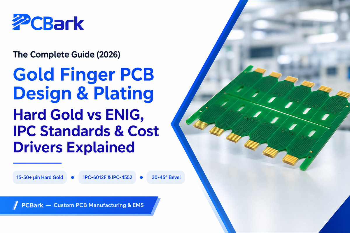
A gold finger PCB is a printed circuit board with hard-gold-plated contact pads along one edge that slide into a card-edge socket, carrying signals between boards. This guide covers the material science, plating standards, and design rules gold finger PCB manufacturers follow, the engineering behind PCBark’s gold finger PCB capability page, one level deeper.
Quick Specs
| Hard gold thickness | 15–50+ microinch (µin), application-dependent — 0.38μm to 1.27μm in metric terms |
| Nickel underlayer | 100–200+ microinch, or 2.54μm to 5.08μm |
| Typical insertion life at 30µin gold | roughly 200–1,000 cycles (varies by contact force and plating quality); heavier plating rated to 10,000+ cycles |
| Bevel angle | 30–45° |
| Governing standards | IPC-6012F (board qualification), IPC-4552 (ENIG), IPC-A-610 (assembly acceptance) |
| Minimum spacing to PCB outline | ≥1.0mm |
What Is a Gold Finger PCB? Definition, Terminology & Disambiguation
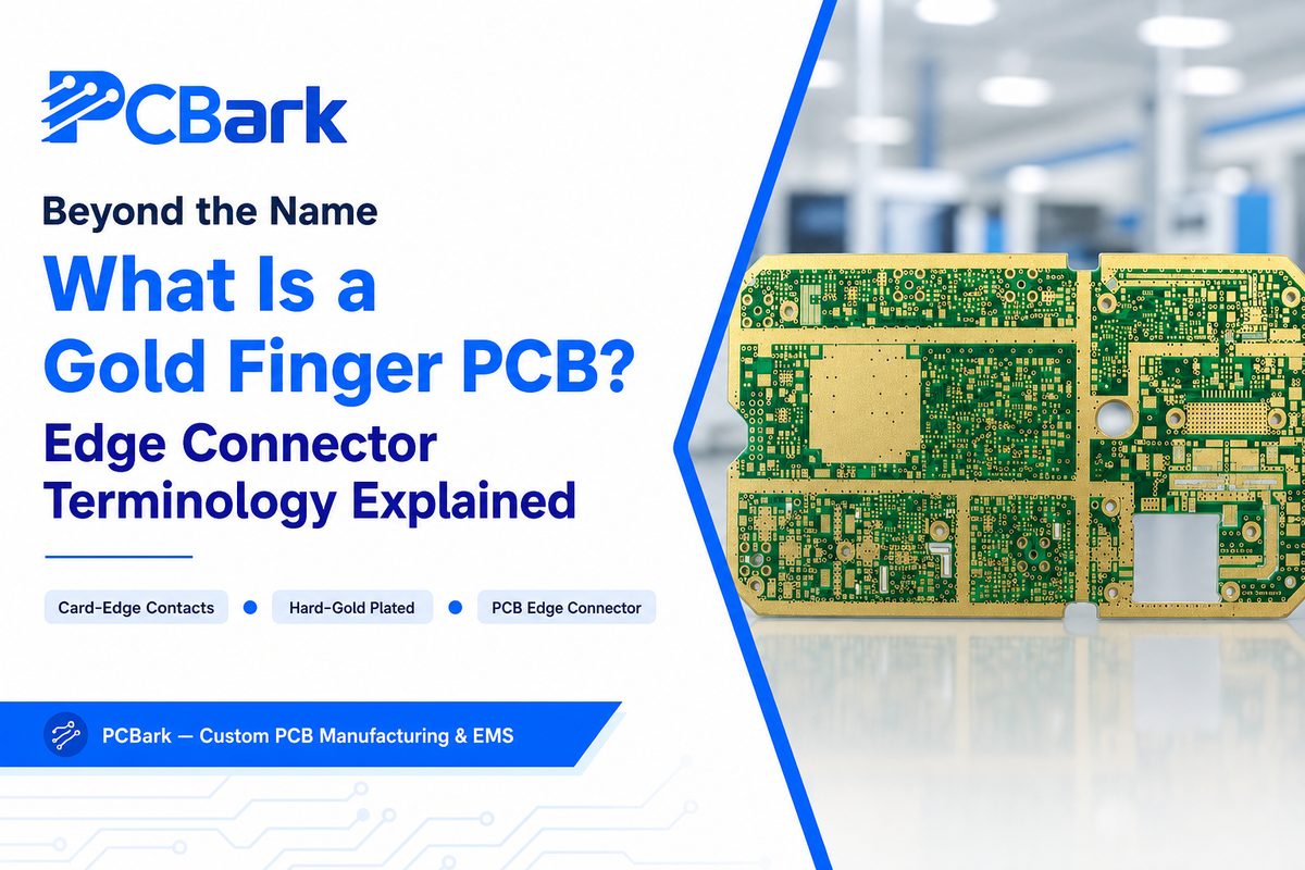
Gold finger PCB pads, also called card-edge contacts or PCB edge connectors, are the gold-plated contacts along a board edge that insert into a matching card-edge socket to transmit signals between printed circuit boards. This naming convention comes from how the pads line up on the edge like fingers on a hand.
A real-world electronics specification for the next-generation Very Large Array radio telescope uses that exact edge-connector arrangement and explains the material choice the same way this guide does. (“Gold finger” also names a 1960s spy thriller and a line of nail polish, so stick to “PCB gold finger” in RFQs to be perfectly clear.)
Many electronic devices employ gold connectors; however, gold finger PCB manufacturing is one of the world’s highest-volume applications of this technology. Electrically, the purpose of gold fingers on printed circuit boards is their conductivity, and most importantly, that gold doesn’t oxidize readily upon contact with air the way other materials like nickel or bare copper do. Without that one key benefit, the material expense of gold would rarely justify using it in this most inexpensive area of the PCB design. Oxide-based connection failures can be silent but occur long before visible signs, so the lack of oxidation afforded by gold virtually eliminates this failure mode.
| Term | Where you’ll see it |
|---|---|
| Gold finger / Golden finger | Most common in fabrication quotes and Asian manufacturer documentation |
| Edge finger / Edge contact | Common in North American design guides (e.g. Sierra Circuits) |
| Card edge connector | Connector-industry term, describes the socket and board pair together |
| PCB edge connector | Generic catch-all, also used loosely for non-gold edge contacts |
Gold fingers provide a reliable electrical connection because pure gold resists the oxidation that plagues lesser metals. PCB gold fingers are the gold-plated connectors engineers rely on for frequent plugging and unplugging without failure, and separately, fingers are gold-plated connectors under every major standard covered in this guide — you connect the PCB to peripheral devices through a slot on the motherboard, and the fingers and edge geometry has to align precisely. Gold is used specifically for its purity, and gold is solid enough to resist wear across the 2 to 50 microinches range most designs specify. That adhesiveness of the gold plating to the underlying nickel is what keeps the connection durable over the product’s service life. Good design of gold fingers also has to account for the cost of gold plating, since electric gold pricing tracks the commodity market — segmented gold fingers and long-short gold layouts (uneven pad lengths, occasionally called short gold sections near the edge chamfer) exist specifically because they are easier to solder and inspect than one continuous run, a pattern documented in publicly available design guides from fabricators including JLCPCB. That process of PCB gold plating means PCB gold fingers also serve a mechanical alignment role beyond signal transfer — PCB gold fingers are also specified per whichever IPC class the end application calls for, and applications of gold in this context span everything from expansion cards to backplane connectors.
Hard Gold Plating Specifications: Thickness, Composition & Insertion-Cycle Tiers
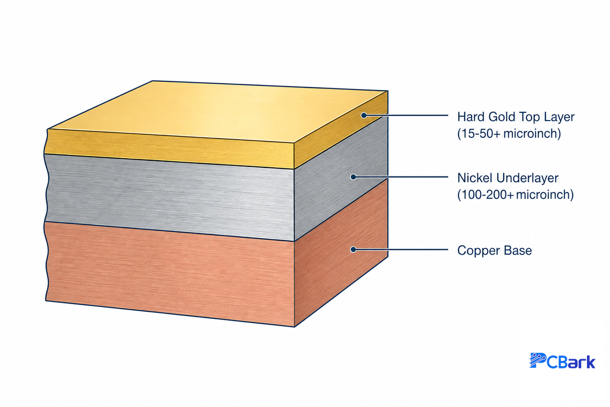
On printed circuit boards, hard gold plating will always be electroplated onto the nickel underlayer – the plating will never be just a bare copper finish, a sequence documented in issued gold-finger fabrication process patents as well as in every major fabricator’s own process spec. An electroless or electroplated nickel layer is applied between the copper and the hard gold to prevent the two from interacting over time and provide an underlying structural support to the contact pads; for the best electrical and wear characteristics on your next PCB design, PCBs can be manufactured with a nickel thickness of over 100 microinches and a gold plating of over 15 microinches depending on your requirements.
When a drawing calls out “30 microinches” of thickness on a gold finger, that specification means much more than you might assume at face value. Hard gold is itself subject to ASTM B488, a performance specification aimed at engineering-use of gold coatings of a minimum 99.00% purity and a nickel under plating, commonly of 2.5μm to 5μm. For printed board finishing processes and product designs, however, IPC-4552, currently at Rev.
B (a 2021 revision, with tighter corrosion-resistance requirements), defines the standard performance parameters for both immersion- and hard-gold finishing processes on PCBs. IPC-4552, with its 1.5mm x 1.5mm standard measurement spot size, dedicates an entire chapter to calibration standards, gauge repeatability studies, and guard band tolerances, so that a “30 microinches” spec call-out will be understood to have the same meaning on every PCB fab shop floor, not just as an aspirational target. Indeed, even appendices within IPC-4552 document inter-lab and inter-instrument comparisons, in recognition that x-ray fluorescence (XRF) readings for the same amount of actual physical deposit may vary between measurement tools and operators.
In contrast, PCBark has production tolerances that constrain its pitch spacing to 0.50–0.30mm, with impedance held to within ±10% to ±5% depending on board tier. These gold finger measurement tolerances are the mechanism by which that down-stream process control gets maintained.
| Duty tier | Hard gold thickness | Typical rated insertion cycles |
|---|---|---|
| Light duty / prototype | 3–15 µin | Low; not intended for repeated field mating |
| Standard commercial | ~30 µin | Roughly 200–1,000 cycles (source estimates vary with contact force and plating quality) |
| High-reliability | 50 µin | Up to several thousand cycles |
| Maximum spec | Heaviest commercial plating | Cited up to ~10,000 cycles by some fabricators |
📐 Engineering Note
The range of 200 to 1,000 insertion cycles for 30- microinch gold plating in published specifications is also far from precise — at least one independent fab shop reference claims 200 to 500 cycles for 30 microinches of plating, while another cites around 1,000 cycles. Consider any published number for insertion cycles, without a corresponding contact force and socket mating spec, to be an informal approximation rather than a guaranteed figure and obtain such information from your PCB fabricator for mission-critical designs. Our gold fingers at PCBark range from 2 to 32 layer boards and have service life cycles from 500 to 5,000+ insertions depending on the plating tier specified.
The plating process for gold fingers begins with a PCB prototype run before scaling to full production. Electroplated hard gold is deposited to a specified thickness, then inspected for excess plating or uneven gold buildup along the edges of PCB contacts. Every PCB must pass a series of inspections and defect tests confirming proper finger length and alignment before it ships — engineers check that pads stay neatly arranged at the edge, with length and width are neatly matched and no lengths located at the edge outside tolerance for the size of the PCB. Gold fingers should always maintain a consistent thickness of gold from finger to finger, because those rules are always applicable regardless of layer count. Hard gold exists specifically to withstand the abrasive effects of constant PCB usage; the abrasive effects of constant PCB wear at the edge of the board are exactly what the plating thickness of gold fingers is engineered to resist, and engineers rely on gold fingers to survive those effects of constant PCB usage across the product’s rated life. Boards with solder pads of varying lengths located at the edge of the board — where pads of varying lengths located near pads of different lengths located side by side form the long-short pattern — still need every finger’s width are neatly arranged within the same tolerance band as a flush layout.
Hard Gold vs ENIG: Which Finish for Edge Connectors
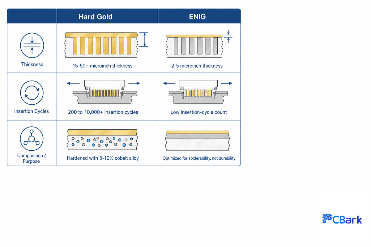
While hard gold and ENIG (Electroless Nickel Immersion Gold) both are gold-plated finishes, they’re designed for fundamentally different applications. ENIG offers a thin layer (roughly 2 to 5 microinches, or 0.05μm to 0.13μm) of relatively soft immersion gold that provides excellent soldering properties for the contact pads. Hard gold provides a thicker electroplated gold alloy hardened with 5–10% cobalt that’s significantly harder in order to withstand repeated mechanical contact.
“The rate of rise in contact resistance between terminal pair members is shown, albeit the underestimation of contact resistance is extremely large in case of small contact normal forces.” A combined experimental and FEM investigation of the reliability of edge contacts of a DDR4 interface under mechanical impact concluded that low normal force, low compliance gold contacts are much more susceptible to contact resistance anomalies than contacts under high force, with firm contact seating.
Huang, T.-C. and Liao, K.-C., Department of Biomechatronics Engineering, National Taiwan University, J. Electron. Packag. 145(1), 2023 (ASME)
ENIG is also a gold-based surface finish, and the relevant IPC specification for it, IPC-4552, includes coverage of “Contact Surface” and “Edge Tab” as applications for the material — making ENIG an approved finish technology, even for board edge contacts. That said, IPC-4552 also carries a “Limitations of ENIG” section, discussing issues including creep corrosion and signal loss in high-frequency applications, which is the standards-compliant version of what field reports from PCB designers and engineers already say.
✔ Hard Gold Advantages
- Withstands hundreds to thousands of insertion cycles
- High wear resistance under mechanical friction
- Standard choice for edge connectors and card-edge slots
⚠ ENIG Limitations for Edge Contacts
- Thinner and softer immersion gold layer (2-5microinches) provides shorter wear life under repeated contact.
- Optimized for solderability, not mechanical durability
- IPC-4552 discussescreep corrosion and high-frequency signal loss.
One eevblog forum thread on PCIe edge connector plating sums up the design decision rule quite simply: “it really is all about the cycles the connector will see in its life.” Remember that quote! That’s the right way to think about it- not “is ENIG bad”, but “how many mating cycles does this connector need to stand up to?”
The Insertion-Cycle Cutoff
| Expected lifetime mating cycles | Recommended finish |
|---|---|
| Under ~50–100 (assembled once, rarely re-seated) | ENIG is generally acceptable |
| Roughly 100–500 (occasional field service, module swaps) | Light hard gold (15–30µin) |
| 500+ (frequent hot-swap, test fixtures, expansion cards) | Standard-to-heavy hard gold (30–50+µin) |
Cycle bands are directional, built from the cross-referenced sources in this guide’s engineering notes, not a single published IPC table – check against your exact connector and intended usage before finalizing a spec.
Want the full breakdown of what PCBark can build to, tier by tier? Check out the gold finger PCB capability matrix for RFQ-ready specification ranges.
Beveling, Chamfering & Design Rules for Gold Finger Layout
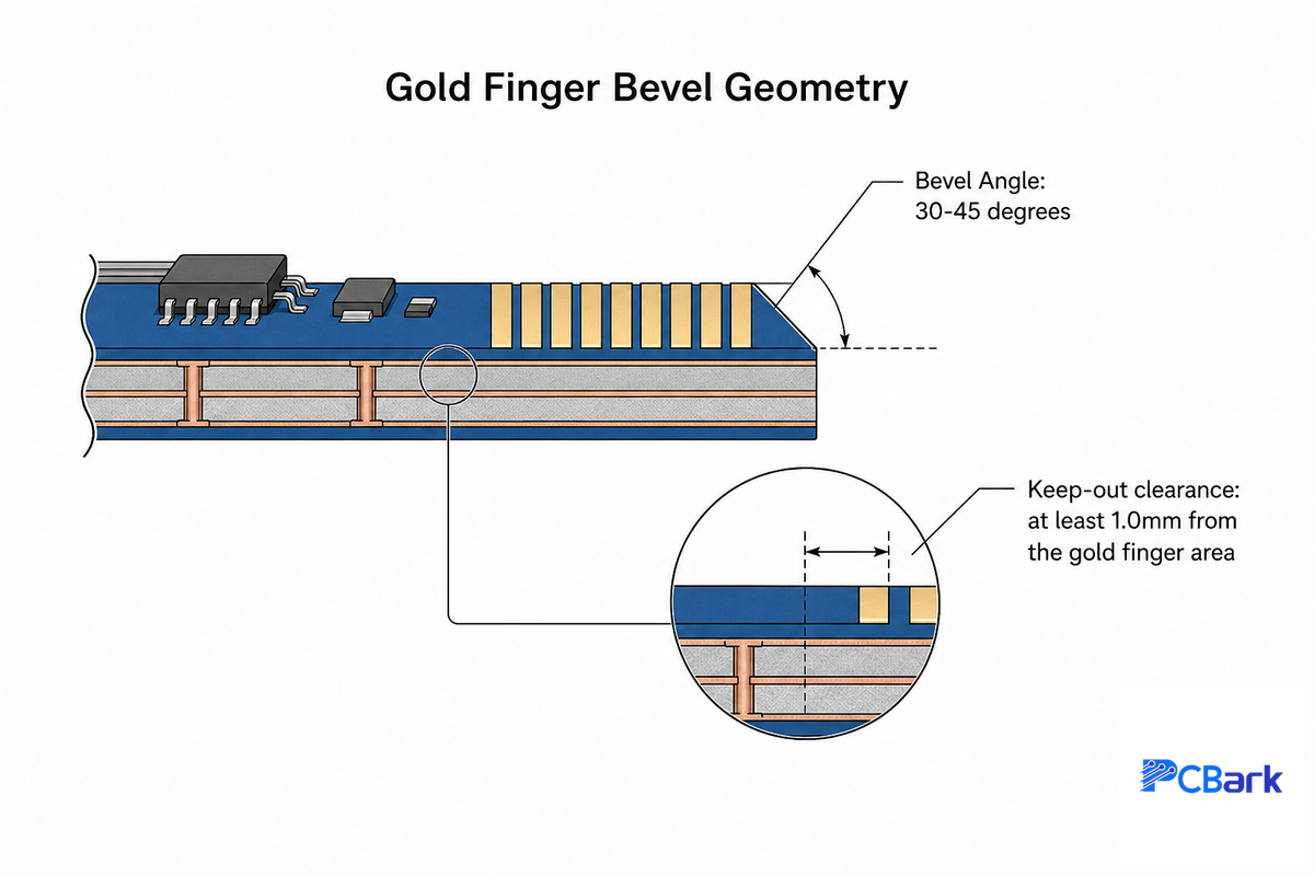
Getting the plating spec right doesn’t help if the board won’t physically seat in its socket. Gold finger edges are beveled – cut at an angle rather than left square – so the board can slide into the mating connector without the leading copper edge catching or gouging the socket contacts. Three independent fabricators’ design guides converge on the same range: 30-45 degrees, with the bevel always facing away from the center of the board — the exposed edge is also where corrosion protection matters most, which is why post-plating corrosion-resistance treatments for gold fingers specifically target this beveled contact zone.
- Keep plated through-holes, solder mask, and screen printing at least 1.0mm from the gold finger area
- Route inner copper layers clear of the board edge under the bevel to prevent copper exposure during beveling
- Keep plated pad length under roughly 40mm per finger; longer runs increase plating-uniformity risk
- Confirm bevel direction and hard-gold pad choice explicitly in fabrication notes, not just the silkscreen
- Solder-joint reliability testing referenced in the connector literature typically cycles boards through 2x reflow profiles plus 8 hours at 72°C/85% RH before evaluating wetting and contact performance
Who Specifies the Bevel Edge and Hard-Gold Pads, Designer or Fab House?
View Answer
Both share the responsibility, and that split trips up more first-time gold finger designs than any plating question. Designers own which pads are hard-gold contacts, their length and spacing, and which side the bevel sits on relative to connector polarity, all specified explicitly in the Gerber/CAM files or a written fabrication note.
Fab houses, in turn, own the mechanical execution: the exact bevel angle within the 30-45 degree window, the routing/milling process, and the keep-out clearances around plated through-holes and solder mask. A common failure mode reported by PCB designers on public forums is assuming the fab house will figure out which pads need hard gold, then receiving boards where the wrong pads were plated or the bevel was cut on the wrong edge. Put both specs in writing on the drawing, every time, and confirm the panel-level fabrication note matches the individual board note before the job releases to production, since panelization can silently drop a per-board callout that only lived on one Gerber layer.
IPC Standards & Acceptance Criteria for Gold Fingers
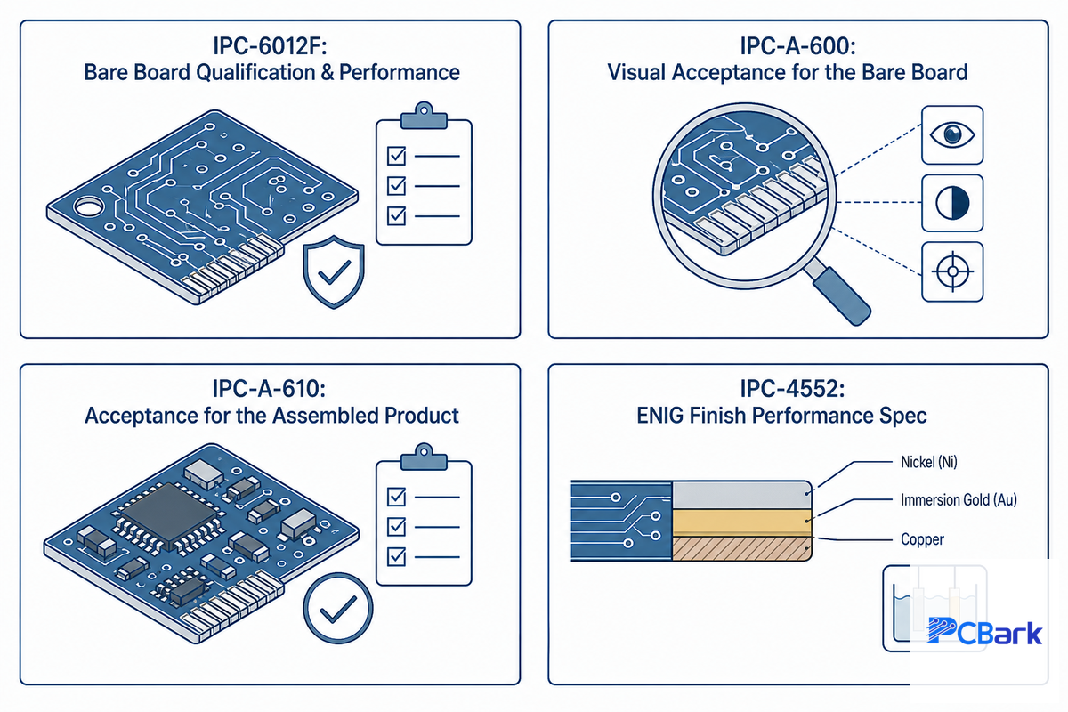
There’s more than one IPC standard related to gold finger boards and mistakenly grouping these two together is an all too common issue for marketing departments of suppliers. IPC-6012F, the current version of this standard which defines the finished bare board qualifications, covers the following two edge connectors: Table 3.5 – “Edge Printed Board Contact Gap” The standard covers edge connectors as follows: – 3.3.8 – Edge Printed Board Contact, Junction of Gold Plate to Solder Finish.
– 3.5.4.4 – Board Edge Connector Lands.
IPC-A-600 is the supporting visual acceptance standard for the bare board, while IPC-A-610 is the acceptance standard for the completed electronic product, it’s a different document to IPC-6012F. Not an older or newer version. IPC-4552 is the ENIG finish specific performance spec.
| Standard | What it governs |
|---|---|
| IPC-6012F | Bare rigid-board qualification & performance, incl. edge connector lands (Class 2/3) |
| IPC-A-600 | Visual acceptance criteria for the bare board |
| IPC-A-610 | Acceptance criteria for the assembled electronic product |
| IPC-4552 (Rev B) | Performance spec for ENIG deposits specifically (thickness, XRF measurement, limitations, corrosion resistance) |
Most gold finger applications typically fall under the IPC-6012F Class 2 standard, while the higher-level Class 3 inspection applies for more mission-critical and high-reliability industries such as aerospace, medical and industrial controls — a federally-indexed engineering paper on FPGA development boards specifically ties IPC 6012B Class 3A requirements to edge connector design, confirming this isn’t just a paperwork distinction. PCBark’s own production process is IPC-A-610 Class 2 and Class 3 certified, with AOI and electrical testing applied at final inspection.
Where Gold Fingers Are Used: Applications & the 3 Gold Finger Types
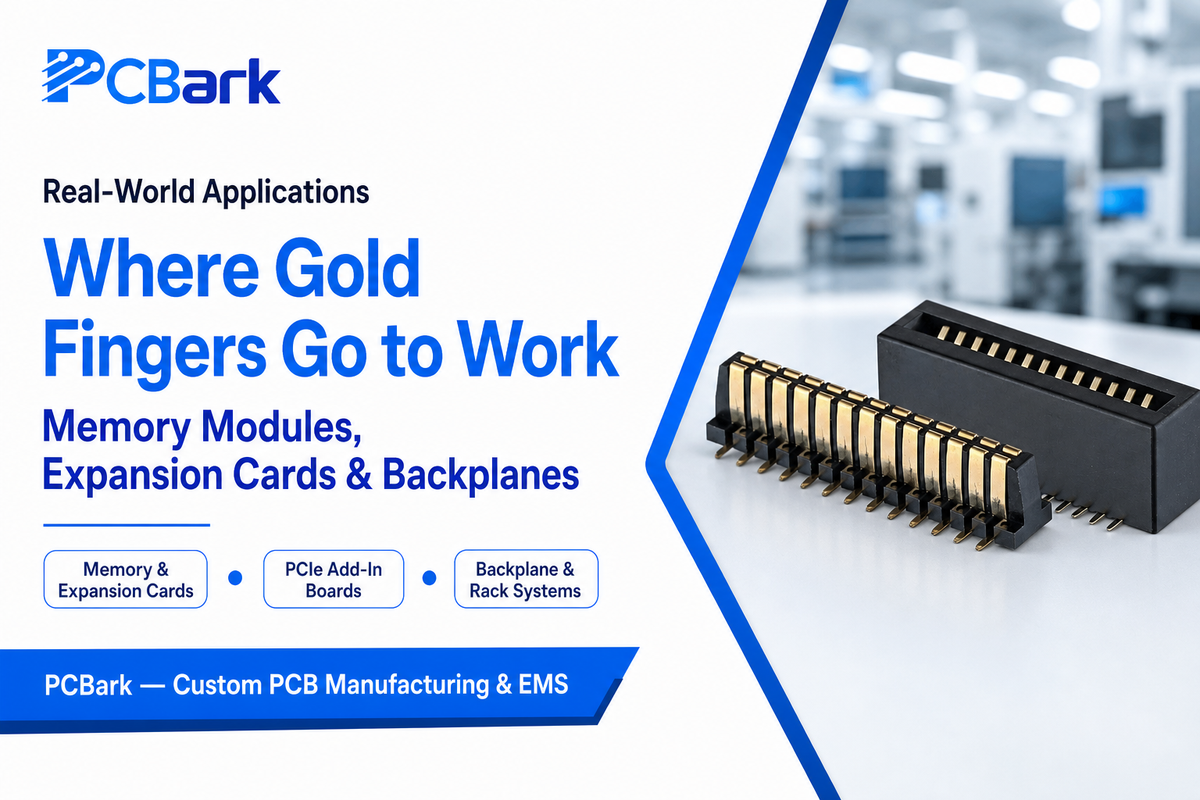
Gold finger edge connectors show up anywhere a secondary board needs to socket onto a primary one instead of using a cable: memory module connectors, graphics and expansion card sockets, PCIe add-in boards, SIM card connectors, battery connectors on portable devices, and backplane or rack cards in industrial and networking systems.
Once a prototype passes limited-run testing, the design usually heads into full-panel PCB production, where finger and plated-area totals are fixed prior to volume runs. High-speed applications push this further still: a Missouri S&T signal-integrity study on gold finger port modeling found the connector geometry itself needs full-wave simulation once channel speeds climb high enough.
| Type | Tier / IPC class | Gold thickness | Typical use |
|---|---|---|---|
| Regular (flush) | Light duty / Class 2 | 3–15 µin | Prototype and low-cycle validation runs |
| Regular (flush) | Standard / Class 2 | ~30 µin | Graphics cards, network cards, general expansion cards |
| Regular (flush) | High-reliability / Class 3 | 50 µin | Industrial backplane and rack cards |
| Long-short (uneven) | Standard / Class 2 | ~30 µin | Memory modules, USB flash drives |
| Long-short (uneven) | High-reliability / Class 3 | 50 µin | Hot-swap server and telecom modules |
| Long-short (uneven) | Maximum spec | Heaviest commercial plating | Frequent hot-swap test fixtures, rated to ~10,000 cycles by some fabricators |
| Segmented (interrupted) | Application-specific | Application-specific | Specialized signaling interfaces with non-contiguous contact zones |
| ENIG (non-hard-gold) | Light duty / Class 2 | 2–5 µin | Low-insertion-count assemblies only, per the Insertion-Cycle Cutoff above |
| Any type | Aerospace / medical, Class 3 | Per IPC-6012XS / IPC-6012XM addenda | Deviation classes layered on top of base IPC-6012F requirements |
Long-short pin arrangement isn’t just aesthetic; they’re designed to sequence the order of contact when a board is being inserted. The longer pin of hot-swapping form factors touches first and separates last to ensure that the sequence of contact remains constant, Ground-contact first, Pre-charge second and Power third. That sequence prevent both the memory board itself and the host system from receiving excessive in-rush currents or floating the ground in live-insertion and hot-removal scenarios-which is precisely the reason that memory modules and hot-swappable cards have the non-flush long-short pin design.
What Drives Gold Finger PCB Cost
Gold finger PCB cost depends on gold-plated area, current gold spot price, insertion-cycle tier, and bevel or edge-routing work, so no single flat percentage markup holds across projects. PCBark quotes gold finger jobs itemized against those factors rather than as a flat adder, because a bundled number hides which lever actually moved the price.
Buyers who lock in a flat percentage markup before quoting often get an unpleasant surprise once the real gold-plated area is measured, because gold spot price, plating tier, and finger geometry move independently of each other and a bundled adder can’t track all three at once. Here is a reasonably good list of the actual cost drivers:
Key Cost Drivers
- Gold-Plated area. One fabricator’s in-house quoting tool alerts about extra costs once gold-plated area goes above about 15% of the board – more fingers, thicker fingers, longer board – all directly drive up gold-plated area.
- Gold spot price exposure. Hard gold plating cost follows the commodity gold market in direct contrast to a copper based surface; a quote fixed weeks apart can move with bullion prices.
- Insertion-cycle tier. More gold and more process time per panel for heavier plating to give a higher mating-cycle rating.
- bevel and edge routing: Beveled edge cut: It’s an added machining process step and it’s a function a regular square-edge panel wouldn’t need.
- Environmental compliance overhead. Precious-metals electroplating (gold included) falls under EPA effluent guideline regulations in the US (40 CFR Part 413, Subpart H is specific to PCBs); waste water treatment and permitting costs at a gold plating line enter the mix of what fabricators will quote even if it doesn’t appear as a separate line item.
A 100mm-wide edge with 40 fingers at 1.0mm pitch will have about four times the gold surface area as the same edge at 0.5mm pitch with the same finger count – it’s why finger count and finger width are the first place to look for price reductions on an incoming quote. Selective plating (gold only on the finger area, not the whole panel) is the typical method fabricators use to make the finish more cost-effective while still meeting factors 1 and 3; process-patent activity on the subject is still a signal that this finish remains a competitive price battle, not a commoditized, finished process.
Industry Outlook: Is Gold Finger Demand Growing or Being Displaced by ENIG?
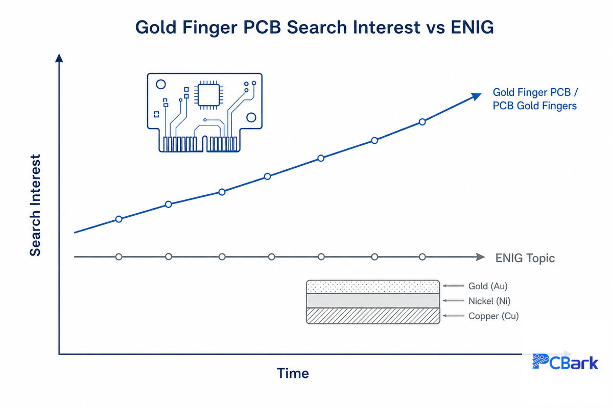
Gold finger demand is not being displaced by ENIG. Search interest for exact terms like “gold finger PCB” and “PCB gold fingers” has trended upward in recent months even as broader PCB-connector search terms trend downward, while interest in the broader ENIG topic has stayed flat over the same period.
This pattern aligns with buyers searching and specifying finish-by-finish rather than by general connector category. Recent selective-area gold electroplating patent activity points the same direction: suppliers are still actively competing on process efficiency for hard gold rather than abandoning it for a cheaper finish.
That said, there was a change in IPC-6012F Rev F, published September 2023, that’s worth noting specifically so that it isn’t over stated: Table 1-2 now specifies that ENIG can be used as the general default board finish in a drawing where no finish is listed, on any drawing issued after Oct 1, 2023. That’s a change to the fallback default of the entire board, not a designation that ENIG has supplanted hard gold on edge connector contact surfaces – the mistake we’d flag for a buyer here is assuming a title-block silent on finish will still land on hard gold the way it might have before 2023. Because that fallback default just moved, an aerospace, medical, or industrial-controls program relying on unstated defaults risks getting an ENIG-finished edge connector engineered for a general board, not the insertion-cycle-rated contact the application actually needs. PCBark’s engineering team flags this gap during DFM review specifically so it isn’t caught at incoming inspection instead. For buyers in 2026, the takeaway is to be sure you’re explicitly defining the finish on gold finger drawings and not depending on a fallback.
Ready to Spec a Gold Finger Board
Request a Gold Finger PCB Quote →
Ask Our Engineering Team a Question
Q: What is a gold finger PCB?
See Answer
A gold finger PCB is a hard gold-plated printed circuit board with contact pads running along one edge, connecting to a card-edge socket to transmit data between boards. In a PCB design or an RFQ, the term refers specifically to the edge connector’s plating, most commonly on a 2-32 layer board with a 0.50-0.30mm finger pitch.
It differs from the fingernail-polish brand, the 1960s spy film, or the slang term used in electronics recycling, each of which will surface in an unfiltered web search for the same phrase.
Q: How thick should gold finger plating be?
View Answer
Commercial gold finger boards typically use approximately 30 microinch (0.76μm) of hard gold over the nickel underlayer, which fabricator estimates put at between 200 and 1,000 mating cycles depending on contact pressure and plating quality. Thinner platings down to 15µin serve low-cycle prototype or light-duty service.
Heavier platings, as high as 50µin and beyond, go into high insertion-cycle designs such as test fixtures or frequently-serviced modules, with some fabrication houses rating their heaviest common plating up to approximately 10,000 cycles. Because published cycle figures are informal fabricator estimates rather than a single IPC-mandated table, always confirm the exact thickness tier and expected mating-cycle count with your fabricator’s own engineering team before finalizing a mission-critical spec.
Q: Why is gold used instead of other metals for PCB edge connectors?
View Answer
Gold offers good electrical conductivity with a strong resistance to oxidization. The metals most frequently found beneath gold platings, copper and bare nickel, both develop a film of oxide in air; that oxide layer builds an insulating film over time and raises contact resistance even without physical wear, while a plated gold contact does not develop this surface film.
Q: Is hard gold or ENIG better for high insertion-cycle applications?
Read Answer
Hard gold plating is the better choice for high insertion-cycle applications. ENIG’s gold layer is thin (a nominal 2 to 5 microinch) and applied for solderability, not physical durability, so it suits only contacts with a low expected mating-cycle count.
If anticipated mating cycles rise into the hundreds, gold finger contacts commonly specify a plating that is harder and thicker than ENIG, as thick as 15 to 50µin, sometimes fortified with a few percent cobalt. The Insertion-Cycle Cutoff table above gives a starting point by cycle count.
Q: What does a gold finger PCB cost to fabricate?
View Answer
There is no universal, fixed cost per board for gold finger PCB fabrication, since the gold-plated surface area, current spot price of gold, insertion-cycle tier, and the mechanical work of edge beveling all vary considerably between projects and are not standardized across fabricators.
As a guideline, one fabricator applies extra fees once more than approximately 15% of a board’s surface area is gold plated, and controlling finger size and count offers the greatest opportunity to manage cost. Selective plating, gold only on the finger area rather than the whole panel, is the standard lever fabricators use to keep that percentage down without compromising the insertion-cycle rating the design actually needs. Request a detailed, itemized quote rather than a flat rule of thumb.
Q: Can gold fingers be repaired or re-plated after wear?
View Answer
In very limited circumstances, yes. this would constitute a “rework,” however, not a standard repair. Typically, you would have to remove the plated hard gold and underlying nickel plating from the finger area, then re-plate it and still retain original mechanical clearances and bevel dimensions. It’s almost always more economical in production volume to replace a board than it is to re-plate it.
References & Sources
- IPC-6012F: Qualification and Performance Specification for Rigid Printed Boards – IPC
- IPC-4552: Performance Specification for ENIG Plating for Printed Boards (current edition Rev B, 2021) – IPC
- ASTM B488: Standard Specification for Electrodeposited Coatings of Gold for Engineering Uses – ASTM International
- Experimental and Numerical Investigations of Intermittence for Electronic Connectors Subjected to Mechanical Shocks – Huang & Liao, National Taiwan University, J. Electron. Packag. (ASME), 2023
- Electroplating Effluent Guidelines – U.S. Environmental Protection Agency
- Simplified Equivalent Golden Finger Port Setup for Fast and Accurate 3D Full-Wave Simulation for High-Speed Channels – Missouri University of Science and Technology
Related Articles
- Ceramic PCB Guide – materials science and DFM for ceramic substrates
- Heavy Copper PCB Guide – differential etching and current-carrying capacity
- Rogers PCB Guide – RF substrate selection and Dk/Df fundamentals
- Aluminum PCB Guide – metal-core board design and thermal management
About This Analysis
This guide blends PCBark’s production plating and nickel-underlayer capability data with cross-checked IPC standards documentation, a peer-reviewed connector-reliability study and EPA regulatory filings since gold finger design decisions get made from RFQ drawings, not marketing copy. Where fabricator sources disagreed on insertion-cycle figures for the same nominal thickness, we reported the range rather than picking the more favorable number. Reviewed by the PCBark technical team