Get in touch with PCBark Company


A Rigid-Flex PCB Manufacturer is a fabricator that builds boards combining rigid FR-4 sections with flexible polyimide circuits in one continuous structure, qualified under IPC-6013E and designed to IPC-2223E. The quick reference below covers the core specs; the sections that follow cover materials, fabrication, standards, and reliability in depth.
Quick Specs
| Governing qualification spec | IPC-6013E (current revision, September 2021) |
| Governing design spec | IPC-2223E |
| Typical bend radius (multilayer) | 10-15x board thickness |
| Dynamic flex foil | Rolled-annealed (RA) copper, >1,000,000 cycles at 5mm radius |
| Static flex foil | Electrodeposited (ED) copper acceptable, <1,000 cycles at 5mm radius |
| Flex substrate | Polyimide film, stable from -200°C to 400°C (Kapton is DuPont’s trade name for the material class) |
| Typical inner/outer trace-space | 2mil / 2mil (industry-typical capability, confirm per fabricator) |
| Typical drilling/PTH tolerance | ±0.05mm (industry-typical capability, confirm per fabricator) |
| Rigid-flex overall thickness range | 0.25mm – 6.0mm (industry-typical capability, confirm per fabricator) |
| Typical flex-zone copper weight | 0.5oz – 2oz (industry-typical capability, confirm per fabricator) |
| Typical build time | 7-20 days production, 1-2 days for RFQ turnaround; quick-turn options as fast as 1 day exist at some fabricators (industry-typical, confirm per fabricator) |
A Rigid-Flex PCB Manufacturer builds boards in a single continuous piece, attaching flexible polyimide circuits between rigid FR-4 pieces so there’s no need for the connectors and cables you’d otherwise need between separate rigid board assemblies. That single detail is the primary reason the aerospace, medical, and automotive engineers specify rigid-flex instead of board-plus-cable assemblies in any application exposed to vibrations, flexing, or that must fit in a compact space.
rigid-flex pcbs are qualified to IPC-6013E while designing under IPC-2223E. I’m noting those differences because almost every manufacturer site lumps the two together and says the board is “IPC compliant”. IPC-6013E is where the qualification standards and design types (e.g. rigid board Type 1 to 4 and Class 1 to 3(S) where 3(S) indicates an enhanced level of control), and IPC-2223E is the set of specific design rules required in order to achieve IPC-6013E qualification. Many “IPC certified” boards aren’t even designing to IPC-2223E.
What Is a Rigid-Flex PCB?
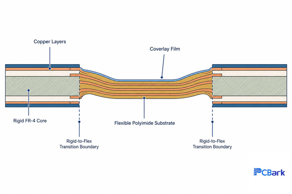
A rigid-flex pcb is one continuous circuit where flexible polyimide circuit layers join rigid FR-4 sections, replacing the cables and connectors that would otherwise link separate rigid boards. Flexible portions fold once at assembly (static flex) or bend repeatedly in operation (dynamic flex), while rigid sections mount high-density components and connectors and carry higher current.
Flexible sections carry the low-power interconnects. NASA’s own rigid-flex robotics design methodology paper (Bell, 2022, IEEE) treats this construction as its own structural category with distinct finite-element validation needs, not a mere variant of pure rigid or pure flex design.
A rigid-flex pcb is distinguished from a completely flexible board that has no rigid section at all (like a flex pcb), and also different from a rigid PCB which has a flat cable jumper that would itself be a separate flexible printed cable (FPC), instead of a built-in flex layer using the same copper stack-up. Rigid-flex itself is a compromise between the two. Its rigid section is stiff enough to securely mount the components, while the flex section does away with an assembled cable. Properly classifying the board at the beginning of the pcb design phase is critical as flexible pcbs, rigid circuit sections and rigid-flex sections each have specific manufacturability restrictions associated with them. Getting this wrong is a costly mistake once tooling is cut, and it’s exactly the kind of question PCBark’s engineering team fields before quoting an automotive or medical program, where ISO 9001 and IATF 16949 process control depend on the classification being right from the first DFM review. Whether your team calls it rigid-flex pcb design, flex-rigid pcb, or simply rigid-flex circuit boards, the terminology varies by supplier but the underlying rigid-flex pcb technology is the same. Advanced rigid-flex technology and multilayer rigid-flex construction have both moved well past the simple two-layer designs common a decade ago.
Rigid-Flex vs. Separate Rigid Boards + Cables: The Engineering Case
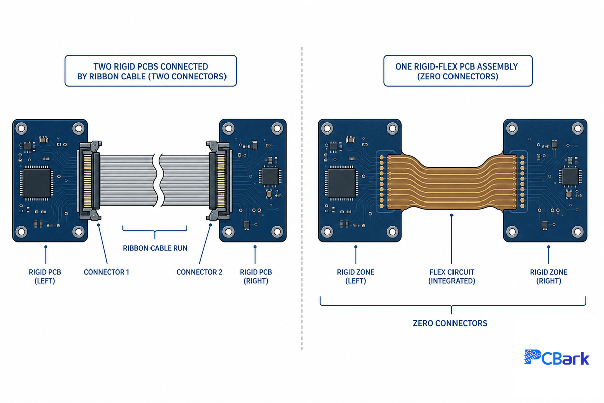
Perhaps the most cited benefit of rigid-flex construction is the elimination of the points where connections occur-and the associated failure modes such as connector corrosion, fretting in the presence of vibration, and strain-relief failures in the cable itself. This is an absolutely valid reason for rigid-flex boards’ appearance in many aerospace and military products which need to be extremely resilient over a multi-year operating life.
“A rigid-flex board can outlast three rigid boards joined by connectors, not because the material is stronger, but because there are zero connection points left to fail.”
But “fewer connectors always equals more reliable” isn’t the full story. US Patent US12382583B2 (NIO Technology Anhui, granted August 2025) demonstrates the reverse engineering intuition applied intentionally: an automotive camera assembly that splits the image sensor and the connector electronics onto two separate rigid boards joined by a flex bridge, specifically so that connector-side mechanical stress and heat don’t transfer into the sensor board and disturb the lens-to-sensor optical alignment. In that design, rigid-flex isn’t chosen to eliminate connectors – it’s chosen to isolate a sensitive rigid island from a noisy one. For a design review, the real question is whether you need rigid-flex to remove failure points, or to isolate domains from each other. Those are different justifications, and they lead to different stackups — conflating them is a mistake that shows up as an unnecessary redesign once the automotive or aerospace program is already in tooling. PCBark’s DFM review is built around asking this question first, before quoting a build. This construction’s reduced space and weight, plus the design flexibility it opens up for the enclosure designer, is why rigid-flex keeps winning out over cable assemblies wherever space and weight are both constrained — but that quality and reliability upside only holds if the isolation-versus-elimination question above was answered correctly first.
Layer Stack-Up Architecture and the Rigid-to-Flex Transition Zone
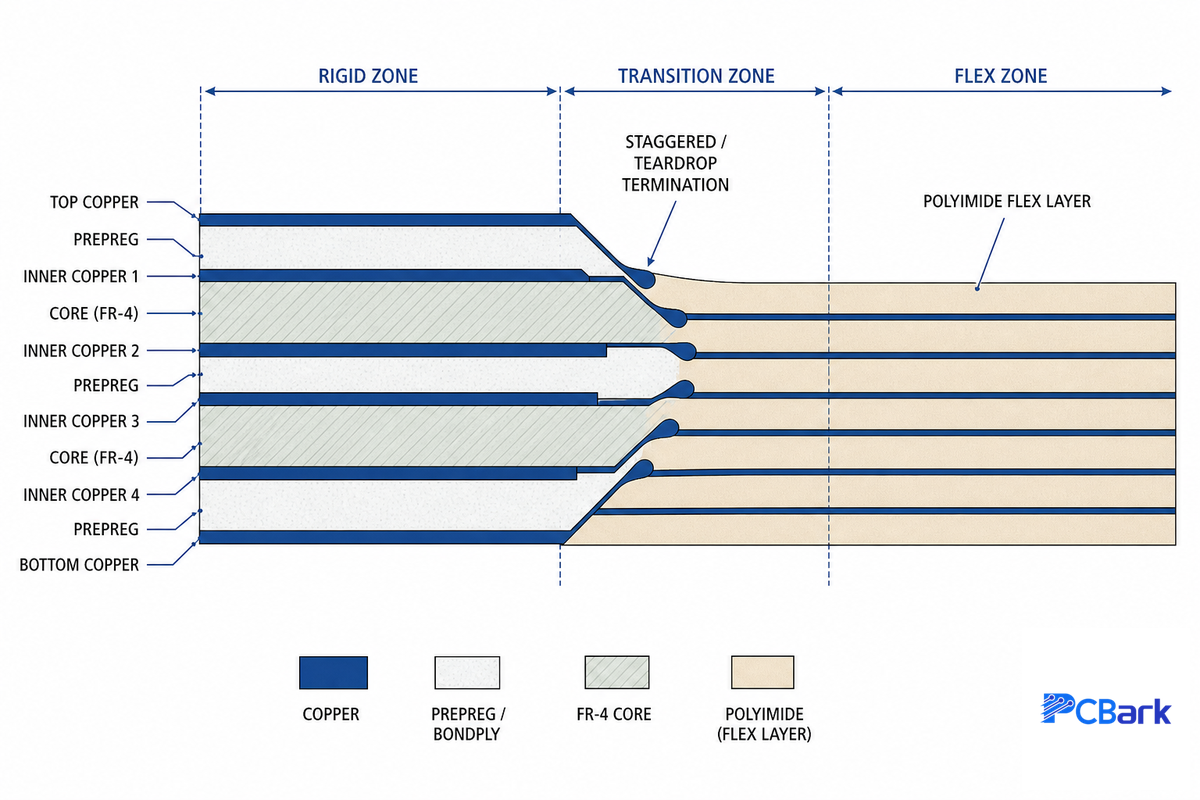
A rigid-flex stack-up is built in zones: rigid zones (FR-4 core plus copper layers, same as a standard multilayer board), flex zones (polyimide film plus copper, protected by coverlay instead of solder mask), and transition zones where the two meet. Transition-zone risk is where most design reviews fall short – not because engineers don’t know it exists, but because, as one fabricator’s design note puts it, transition-zone problems “aren’t always apparent when viewing the Gerber layers alone.” The zone boundary has to be checked against the actual stack-up drawing, not inferred from the 2D layer files — skipping that check is a common, expensive mistake that surfaces as cracked traces only after an automotive or industrial assembly line has already committed to the design. PCBark’s DFM review flags this gap before tooling, not after. A recent manufacturing-method patent, CN119815718B, addresses this exact transition-zone risk for high-aspect-ratio cable-bundle-style rigid-flex construction. Plated through holes in the rigid zones behave the same way they do in standard rigid board fabrication; it’s only the flex-zone plating and coverlay interface that need different process control.
IPC-2223E and IPC-6013E both name specific requirement areas for this boundary that a generic “keep traces away from the bend” instruction misses: hole-to-edge spacing near the rigid-flex boundary, bend-area conductor routing (teardropped pads and staggered – not stacked – conductor positions across adjacent layers to avoid a single crack line), dielectric thickness control between the rigid and flexible regions, and, in IPC-6013E’s more recent language, requirements specific to plated internal layers, dielectric removal at the boundary, and copper-filled microvia structures that now show up in higher-density rigid-flex designs.
📐 Engineering Note
Layer count directly drives minimum bend radius: single-layer flex sections tolerate 3-6x board thickness, double-layer 7-10x, and multilayer flex-in-rigid-flex sections need 10-15x board thickness before the copper is at meaningful crack risk. If your enclosure geometry can’t give you that radius at the specified layer count, the fix is fewer layers through the bend zone, not a tighter radius spec.
Flex Substrate Materials: Polyimide, Kapton, and Coverlay Systems
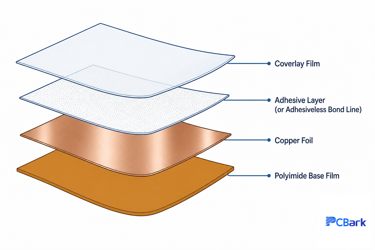
Polyimide film is the flexible layer’s substrate – a polymer chosen for a combination that FR-4 can’t match: it stays mechanically stable and electrically insulating from roughly -200°C to 400°C, which is why flex and rigid-flex circuits show up in borehole logging tools for oil and gas as well as in aerospace applications with wide thermal swings. “Kapton” is DuPont’s trade name for one family of polyimide film, not a separate material category – treat any spec sheet that lists “Kapton or polyimide” as listing the same material twice, and ask the fabricator which supplier’s film and which adhesive system (adhesive-based or adhesive less, like DuPont Pyralux-type constructions) they’re actually quoting.
Coverlay – a polyimide film laminated to the flex copper with adhesive – is also an affect on reliability: it replaces solder mask on flex portions, and its bonding is a common source of coverlay-to-flex delamination if it’s not laminated under a properly controlled cycle. It’s protected by three families of IPC documents covering different aspects, which is a frequent sourcing trap: IPC-4562(R2023) describes the copper foil characteristics (grain structure, thickness tolerances, surface preparation) before it’s applied; IPC-6013E qualifies the final board product; IPC-2223E provides guidelines on how the board should have been designed in the first place. If the fab house can only talk about one family of these documents, it hasn’t truly protected you from this material risk. Flexible material itself also carries a specific durability characteristic worth specifying: flex adhesive systems behave differently from polyimide coverlays when subjected to UV or thermal cycling, and any pcb design ignoring the different materials’ aging behaviours will inevitably lead to long-term coverlay lift. NASA’s GSFC-STD-8001 quality-assurance standard treats this material aging profile as part of acceptance testing, not an afterthought.
How Rigid-Flex PCBs Are Fabricated: The 3-Zone Lamination Sequence
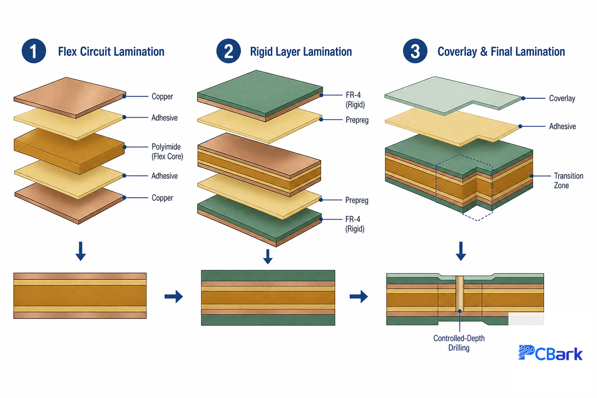
Rigid-flex fabrication runs in sequential stages, not the single lamination pass used for a standard rigid multilayer board. Flex cores are built, tested, and inspected first; rigid layers are then laminated sequentially on top and bottom to keep flex-to-rigid registration consistent between presses, while the transition area is shielded from resin smear at each step.
That sequential process is why rigid-flex tooling routinely costs well over $1,000 even for a modest prototype order — against vendor-quoted 2026 ranges of roughly $1.80-$3.50 per square inch for a 2-layer flex-only board and $12-$30 per square inch for a dense HDI flex design (directional figures, varies by region, volume, and copper pricing) — and why turnaround times run longer than an equivalent-layer-count rigid board once tooling is factored in: each additional press cycle is another registration risk to catch before the next cycle starts, and a misaligned press cycle at any single stage can force a full tooling rebuild rather than a simple rework. Vendors quoting a flat per-square-inch price without breaking out tooling separately are usually amortizing that $1,000-plus NRE into a higher per-unit rate on your first production run, which is worth asking about directly before comparing quotes. Manufacturability review at the pcb design stage — confirming stack-up, transition-zone tolerances, and coverlay cutouts against the fabricator’s actual process, not a generic checklist — is what keeps this multi-stage pcb production run predictable instead of turning into a rework loop, and it’s the single review step most likely to be skipped when a quote is rushed.
💡 Pro Tip
Ask your fabricator to describe the rigid-flex build process in three steps: “flex-core fabrication and testing,” “Sequential rigid lamination” and “Transition zone protection” – prior to submitting Gerbers. Any fab house that simply responds, “we laminate it” is referring to a process designed for a standard rigid product. This process doesn’t include the specialized sequential rigid lamination required for a rigid-flex construction, and is likely the origin of the bookbinder effect and the contamination issues associated with resin bleed from the rigid layers into the flex layer.
Design-for-manufacture helps avoid the “bookbinder effect” – caused by the unequal distance traveled by outer versus inner flex layers during flex transitions, leading to mechanical stress in designs that don’t account for it – by distributing transition zones at different layer locations rather than lining them up in identical X-Y locations. Skipping this review is a recurring mistake in rigid-flex fabrication for automotive and industrial programs, and it’s the kind of risk PCBark’s process engineers check for before quoting a build. Quick turn flex and quick turn flex pcb prototyping services exist specifically to compress the standard 7-20 day production window for low-volume runs, but they don’t skip the sequential lamination steps described above — they compress the queue, not the physics. A recent process patent, CN119893894B, addresses exactly this class of dense multi-board lamination-registration problem.
HDI and Microvias in Rigid-Flex: Where Miniaturization Is Headed
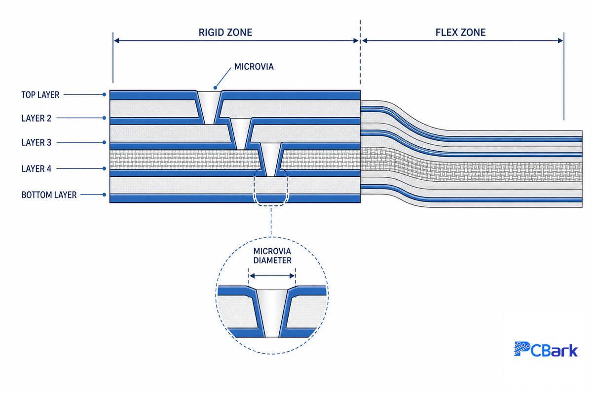
high-density interconnect technologies – laser-drilled microvias instead of mechanically drilled through-holes, any-layer via stacking – are increasingly applied to the rigid sections of rigid-flex boards to push component density up without adding board area. IPC-6013E’s newer language explicitly names copper-filled microvia structures as a qualification consideration, which is a signal that this combination has moved from edge case to mainstream design practice rather than staying a custom, one-off request.
One tradeoff worth knowing before you ask for it: stacked microvias introduce their own thermomechanical fatigue considerations – a stacked-via column concentrates stress differently than a single-depth via, and via reliability testing needs to account for that stack, not just the individual via’s aspect ratio. HDI-in-rigid-flex buys density; it doesn’t remove the reliability-testing obligation, it adds a new failure mode to test for. state-of-the-art laser-drilled microvia equipment closes the gap between rigid-flex pcb fabrication and standard HDI rigid boards, but the qualification burden for flexible pcbs carrying that density is still governed by IPC-6013E, not by the equipment list. Skipping that qualification step on an automotive or medical microvia design is a mistake that can cost a full 1 year requalification cycle after field returns expose the gap, the same class of stacked-structure fatigue risk addressed in CN119893894B‘s dense-board manufacturing method.
IPC-6013 vs. IPC-2223: What Each Standard Actually Qualifies

IPC-6013E is the qualification and performance specification for flexible and rigid-flex printed boards – it defines Type (1 through 4, based on layer construction and rigid-flex configuration) and Class (1, 2, 3, and 3(S) for space applications) and sets the acceptance testing a finished board has to pass. IPC-2223E is the sectional design standard – it defines how the board should be designed in the first place: hole-to-edge spacing, conductor routing through bend areas, dielectric thickness between rigid and flex regions, and general design rules like limiting flex layer count to 1-2 wherever possible for maximum flexibility and lowest cost. That relationship is direct, not parallel: IPC-6013E’s own scope language describes it as covering qualification requirements “for flexible printed boards designed to IPC-2221 and IPC-2223” – 6013 is the exam, 2223 (and its rigid-board counterpart 2221) is the curriculum the board was supposed to be designed against before you sit the exam.
| Type | Construction | Typical Class fit | Buyer signal |
|---|---|---|---|
| Type 1 | Single-sided flexible, no rigid section | Class 1 | Basic consumer flex circuit, minimal inspection, lowest cost tier |
| Type 1 | Single-sided flexible, no rigid section | Class 2 | Consumer flex-only circuit with dedicated function, moderate mechanical demand |
| Type 2 | Double-sided flexible | Class 2 | Higher trace density flex-only, still no rigid island |
| Type 2 | Double-sided flexible | Class 3 | Higher-reliability flex-only circuits, industrial duty cycle |
| Type 3 | Multilayer flexible, no rigid section | Class 2 | Dense flex-only routing, e.g. camera ribbon assemblies |
| Type 3 | Multilayer flexible, no rigid section | Class 3 | High-density flex-only, aerospace/medical-adjacent duty cycles |
| Type 4 | Rigid-flex — multilayer flex plus rigid sections | Class 2 | Standard industrial/automotive rigid-flex, most common commercial tier |
| Type 4 | Rigid-flex — multilayer flex plus rigid sections | Class 3 | True rigid-flex, high-reliability tier; this is the qualification level this guide focuses on |
| Type 4 | Rigid-flex — multilayer flex plus rigid sections | Class 3(S) | Space-application overlay, highest inspection/test rigor, roughly equivalent to MIL-PRF-31032 acceptance rigor |
That last equivalence isn’t a marketing claim – the Defense Logistics Agency’s MIL-PRF-31032 performance specification for rigid, rigid-flex, and flexible printed wiring boards is the mil-spec buyers cite when a supplier’s IPC-6013 Class 3 certification needs a government-recognized anchor, and NASA’s own quality-assurance standard for printed circuit boards (GSFC-STD-8001) requires flexible-board acceptance testing to be performed per IPC-6013 Table 4-3 directly – two independent government sources, not just an industry blog, treating IPC-6013 as the reference qualification document for this board class.
Reliability-test rigor ties directly back to the Class you assign. Class 2 and Class 3 boards per IPC-6013E are verified via interconnect stress testing (IST) – cycled in temperature, measuring resistance change due to the microscopic cracking that precedes a circuit open-and environmental-cycle per the final product application’s requirements. Per NASA technical report on PCB inspection and quality control (NTRS 20180005658), thicker rigid-flex PCBs take more time to dry in processing, and that’s exactly the sort of processing information a Class 3(S) plan has to incorporate but a Class 1 plan doesn’t need. Assigning an IPC-6013 Class 3 designation without specifying which test methodologies should be applied to your specific build is a common means of purchasing a board that will pass paperwork but not your actual field use conditions.
Static vs. Dynamic Flex: Copper Foil Choice and Bend Radius Design Rules
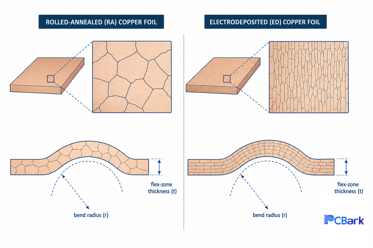
The type of copper foil you select is the single greatest determining factor in the design of a rigid-flex device, depending upon whether your flex bend will be performed only once during assembly (static flex) or repeatedly through out the product’s lifetime (dynamic flex). The greater ductility (20-30% elongation for rolled-annealed [RA] foil versus 10-15% for standard electro-deposited [ED] foil, per published fatigue-testing research using astm E796 and IPC-TM-650 methods) of RA copper directly corresponds to many orders of magnitude greater cyclic bend fatigue life, corroborating reports from fabricators which suggest less than 1,000 cycles for ED foil versus over 1,000,000 for RA at equivalent bend-radius. You can treat the precise multiplier as a value which is dependent upon both foil supplier and thickness, but not as a universal constant.
⚠️ Important
That 1,000x ratio, at matched foil thickness and bend radius conditions, isn’t an absolute value that can be cited outside of your specific build-up. Cyclic bend fatigue life for thin copper foils, based on experimental results from research into such fatigue life testing, depends upon film thickness and grain size as well as RA or ED category, but this factor may be reasonably approximated. The rule of thumb is that RA lasts a factor of 1,000 times longer than ED; consult the specific thickness and fabricator-supplied foil vendor data when you’re out of the initial design concept phase.
This is the RA-vs-ED Fatigue Divide in practice: if the flex bend occurs once, and only once (when your part is flexed to assemble it into the final product casing, for instance), ED copper is an acceptable and cost-effective option. But if your flex flexes regularly throughout product use (a camera aperture, an articulating hinge, etc.), you’ll need RA foil and need to expect to pay a premium to get it. If you make the mistake of going the other way, you’ll join a substantial contingent of engineers in being listed among the designers who have made this error.
Bend radius is similarly buyer beware. It’s common to hear 6-10x the flex section total thickness as a rule of thumb for minimum bend radius, and PCBWay themselves has published a table for their capability, 3-6x for single layer flex, 7-10x for double layer, and 10-15x for multilayer flex-in-rigid-flex. I’ve heard Field Engineers in practitioner forums mention the rule of thumb isn’t strictly true in the real world–some consumer hinge devices visibly bend tighter than a strict 6-10x calc would indicate–usually this means the fab cut corners in a few areas–thinner foil, smaller overall flex thickness, and a shorter warranted cycle life than a general-purpose design should carry. NASA’s rigid-flex robotics design paper validates bend-radius and fatigue assumptions with finite-element analysis rather than rule-of-thumb multipliers alone.
📐 Engineering Note — Worked Example
A 4-layer rigid-flex design will have a flex-zone total thickness of 0.20mm (0.008″). Using the multilayer multiplier of 10-15x, your minimum bend radius would be 0.20mm × 10 to 0.20mm × 15, or 2.0mm to 3.0mm. If your enclosure design limits you to a 1.5mm bend radius at that thickness, then instead of forcing your 4-layer stack through an impossibly tight bend that copper won’t be rated for, drop the flex-section in the bend to a 2-layer (7-10x multiplier, 1.4mm-2.0mm min radius).
Where Rigid-Flex Is Used: Aerospace, Medical Wearables, Automotive

Aerospace and defense assemblies use rigid-flex to eliminate connector-based cable assemblies, an ongoing maintenance problem under vibration and thermal cycling — IPC-6013E’s Class 3(S) qualification exists specifically for this segment. Medical devices — imaging probes, hearing aids, wearable monitors — are prime users where space is tight and the assembly can’t easily be serviced; wearables touching skin also need ISO 10993-1 biocompatibility certification, separate from the IPC qualification.
Automotive counts among the largest adopters, for both camera modules (ADAS) and battery management systems. As mentioned, the NIO patent (US12382583B2) is a case of automotive engineers explicitly choosing a two-board-plus-flex-bridge design for the mechanical and thermal isolation it gives the camera sensor by separating it from the connector electronics. Consumer electronics and telecom hardware round out the high-volume corner, where rigid-flex carries a higher per-board cost but meaningfully reduces assembly cost and product footprint. Across all these industries, the common requirement for flexible pcbs and rigid-flex pcb is the same: replace an otherwise unacceptable connector or cable assembly failure point.
What to Ask a Rigid-Flex Fabricator Before You Commit

Once the technology decision is made, sourcing is a separate conversation from the design questions covered above. At minimum, confirm four things: which IPC-6013E Type and Class they regularly qualify to (not just “IPC compliant”); whether they specify RA or ED foil for your flex zone and why; how they describe their lamination sequence (a true 3-zone sequential build, not one step); and what reliability test data they can show for boards at your Class level.
Whether you’re evaluating PCBWay, Sierra Circuits, TTM Technologies, or a smaller shop advertised as built “right here in the USA,” the same four questions apply regardless of the marketing. A fabricator who can address all four with specifics — not vague “quality flex” or “best quality, fast turnaround” salesmanship — is one worth quoting; skipping this vetting is a common, expensive mistake that only surfaces after an automotive or medical program has already committed to tooling.
Whatever stage your pcb project is at, from early product development through a fabricator’s design capabilities review, confirm whether their team of engineers can both manufacture and assemble the finished board in-house, or whether that’s a separate handoff — and whether their “rigid-flex solutions” or general “pcb solutions” page can actually answer your specific pcb needs with data, not adjectives. The full capability specifics — build envelope, layer count range, DFM-to-functional-test turnkey — are laid out in PCBark’s rigid-flex PCB manufacturing and build-envelope page, along with a tier-based capability matrix and reliability cost/decision tree for this evaluation, benchmarked against the same qualification classes documented in USPTO filing US12382583B2.
Industry Outlook: HDI-Microvia Convergence and What’s Next
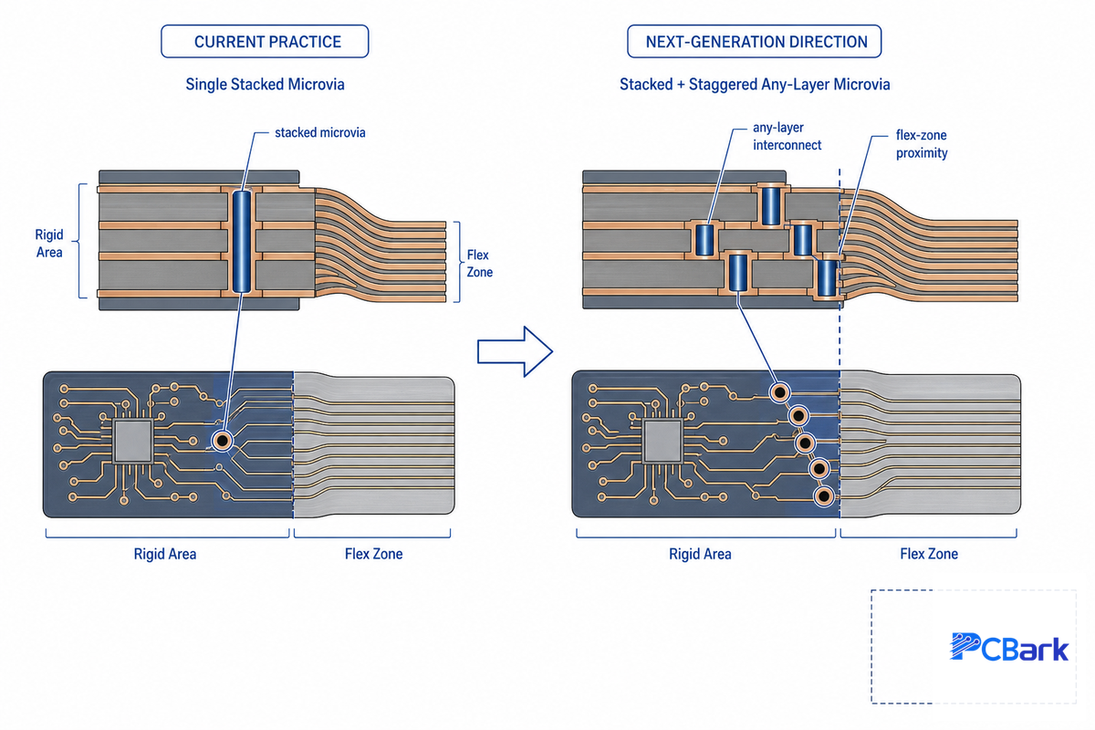
HDI microvia integration into rigid sections of an otherwise-normal rigid-flex is clearly the dominant near-term design trend for the class – all-layer microvias, integrated components on the rigid areas of an all-layer flex design, all of this driven by the same pressures towards miniaturization that will fuel HDI growth broadly across IoT, medical electronics, ADAS, and 5G into 2026. From the buyer perspective, a key implication is that the purchasing requirement for a “rigid-flex fabricator” and an “HDI fabricator” is converging. In short, you’re no longer buying two different skill sets, you’re buying the more complete, more capable one. You’re also buying something that requires a new set of qualification tests on stacked microvias structures to address their own unique thermomechanical fatigue, as this can’t be simply inherited from the existing reliability record for either pure HDI or rigid-flex alone — assuming otherwise is a costly mistake that only shows up as a field failure after an automotive or medical program is already in production. PCBark and other IATF 16949-certified fabricators qualify this convergence explicitly rather than assuming it. (Market-size projections for HDI and rigid-flex growth vary substantially between research providers and are illustrative at best, not a substitute for specific design qualification data.) NASA’s forward-looking rigid-flex design research points the same direction: structural validation methodology, not raw market size, is what will keep pace with the convergence.
FAQ
Q: What Is a Rigid-Flex PCB?
View Answer
A rigid-flex pcb is a single integrated board joining rigid FR-4 sections with flexible polyimide circuit layers, replacing the cables and connectors a design would otherwise need. It qualifies under IPC-6013E and is designed per IPC-2223E, with the flexible zones routing signals through tight or folded spaces.
Q: What Differentiates Rigid-Flex PCBs from Normal (Rigid) PCBs?
View Answer
The structure of a conventional rigid PCB, typically manufactured using all FR-4 material, precludes any folding without substrate cracking or delamination of the copper traces. A rigid-flex pcb integrates flexible polyimide zones with rigid FR-4 sections, allowing portions of the board to fold once at assembly or repeatedly during operation, while still holding components and dissipating heat like a standard board — a distinction that matters most once an enclosure calls for one continuous connection across a hinge.
Q: What Is the Difference Between a Flex PCB and a Rigid-Flex PCB?
View Answer
A flex pcb is entirely flexible, with no rigid sections and typically no support for heavier components without an added stiffener. A rigid-flex pcb combines both: rigid FR-4 for components and connectors, flexible sections where the design needs to bend or fold.
Q: Are Rigid-Flex PCBs Suitable for High-Reliability Applications?
View Answer
Yes — IPC-6013E Class 3 and Class 3(S) exist specifically for high-reliability and space applications, with acceptance testing treated as roughly equivalent in rigor to the DLA’s MIL-PRF-31032 mil-spec. That’s why rigid-flex shows up so often in aerospace, defense, and medical-device programs.
Q: Which IPC Class Should I Specify for a Rigid-Flex Design?
View Answer
Class 2 covers most industrial and consumer designs, where a field failure is inconvenient but not catastrophic. Class 3 fits applications where failure is expensive or dangerous to service after deployment — automotive safety systems, medical devices, industrial control — and Class 3(S) is reserved for space and defense. The Class you specify should also set which reliability test methods your fabricator runs; specifying the Class without confirming the test plan is a common gap.
Q: How Many Bend Cycles Can a Rigid-Flex Board Survive?
View Answer
It depends almost entirely on copper foil choice at a given bend radius: standard ED copper foil typically cracks before 1,000 cycles at a 5mm bend radius, while RA copper foil under that identical radius condition can exceed 1,000,000 cycles. Grain structure and foil thickness also affect the exact number, so treat these as order-of-magnitude planning figures and confirm actual cycle-life data with your fabricator for your specific foil and thickness before committing to a dynamic-flex zone design.
The Team Behind This Report
This guide was compiled from IPC’s own standard scope documents, NASA and Defense Logistics Agency technical references, published copper-foil fatigue research, and current USPTO filings on rigid-flex construction, cross-checked against the design-error patterns most frequently cited across fabricator technical literature for bend-radius miscalculation and foil selection. Reviewed by the PCBark technical team.
References & Sources
- GSFC-STD-8001, Standard Quality Assurance Requirements for Printed Circuit BoardsNASA Goddard Space Flight Center
- Printed Circuit Board Inspection and Quality ControlNASA Technical Reports Server
- MIL-PRF-31032, Printed Circuit Board/Printed Wiring Board General SpecificationDefense Logistics Agency
- Experimental characterization of rolled annealed copper foil fatigue behaviorGirard et al., HAL Open Science
- Fatigue Behavior of Thin Cu Foils and Cu/Kapton Flexible CircuitsResearchGate (ASTM E796 / IPC-TM-650 methodology)
- US12382583B2, Two-Board Rigid-Flex Printed Circuit Board for Automotive CamerasUSPTO / NIO Technology Anhui Co Ltd
- Connect the Dots: Five Best Practices for Designing Flex and Rigid-Flex PCBsI-Connect007
- Rigid-Flex vs. Traditional PCBs: Making the Right ChoiceAll About Circuits
Related Articles
- Rigid-Flex PCB Manufacturer, Build Envelope, Capability Tiers & DFM to Functional TestPCBark’s full capability and procurement guide for rigid-flex fabrication