Get in touch with PCBark Company


Updated June 2026 · Reading time ~13 min.
PCB assembly is the process of mounting and soldering electronic components onto a bare, fabricated printed circuit board (PCBA)the step that turn a bare board and a pile of components into a working product, and where most avoidable cost, delay, and field failure is decided. This guide walks the printed circuit board assembly process end to end, decodes the IPC quality classes, lists the exact design files an assembler need, maps common solder defects to their root causes, and gives you a clear way to choose between turnkey and consigned sourcing.
Quick Specs: PCB Assembly at a Glance
| Attachment methods | Surface mount (SMT) + through-hole (THT), often mixed on one board |
| Smallest placed part | 0201 (0.6 × 0.3 mm); 01005 (0.4 × 0.2 mm) on advanced lines |
| Placement accuracy | ≈ ±0.05 mm at tens of thousands of parts/hour |
| Reflow peak | ≈ 245 °C (lead-free), ~480 °F |
| Core file set | Gerber + Bill of Materials (BOM) + centroid/pick-and-place (CPL) |
| Acceptance standard | IPC-A-610J (2024), Class 1 / 2 / 3 |
| Soldering standard | IPC J-STD-001J (2024) + Space Addendum for high reliability |
| Core test stack | AOI, X-ray (for BGAs), in-circuit or flying-probe test, functional test |
| Typical prototype lead time | 1–3 weeks, depending on component lead times |
What Is PCB Assembly (PCBA)?
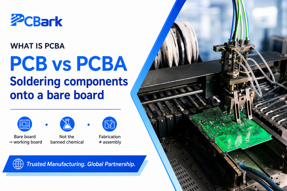
PCB assembly (PCBA) is the process of mounting and soldering electronic components onto a bare, fabricated printed circuit boardresistors, capacitors, integrated circuits (ICs), and connectors, so a circuit design become a working electronic board. PCBA names both the manufacturing process and the finished, populated board, what gets shipped as one of your board assemblies.
Two terms are easy to confuse. PCB fabrication (or PCB manufacturing) builds the blank board from copper-clad laminate, the etched traces, drilled holes, solder mask, and silkscreen. PCB assembly is the next stage: it adds the parts. You can read more about the upstream step in our guide to PCB manufacturing and fabrication, then come back here for the build.
⚠️ One disambiguation
Searches for “why is PCB banned” point at a different “PCB” — polychlorinated biphenyl, an industrial chemical restricted for environmental reasons. In electronics, PCB always means printed circuit board. These two are unrelated.
For a working product, what matters is that the assembled board meet a defined acceptance standard. That standard is IPC-A-610, currently in its 2024 “J” revision, more on the classes below. A useful reference definition lives at the printed circuit board overview, and the broader electronics-standards landscape is maintained by bodies such as IEEE.
The PCB Assembly Process, Step by Step
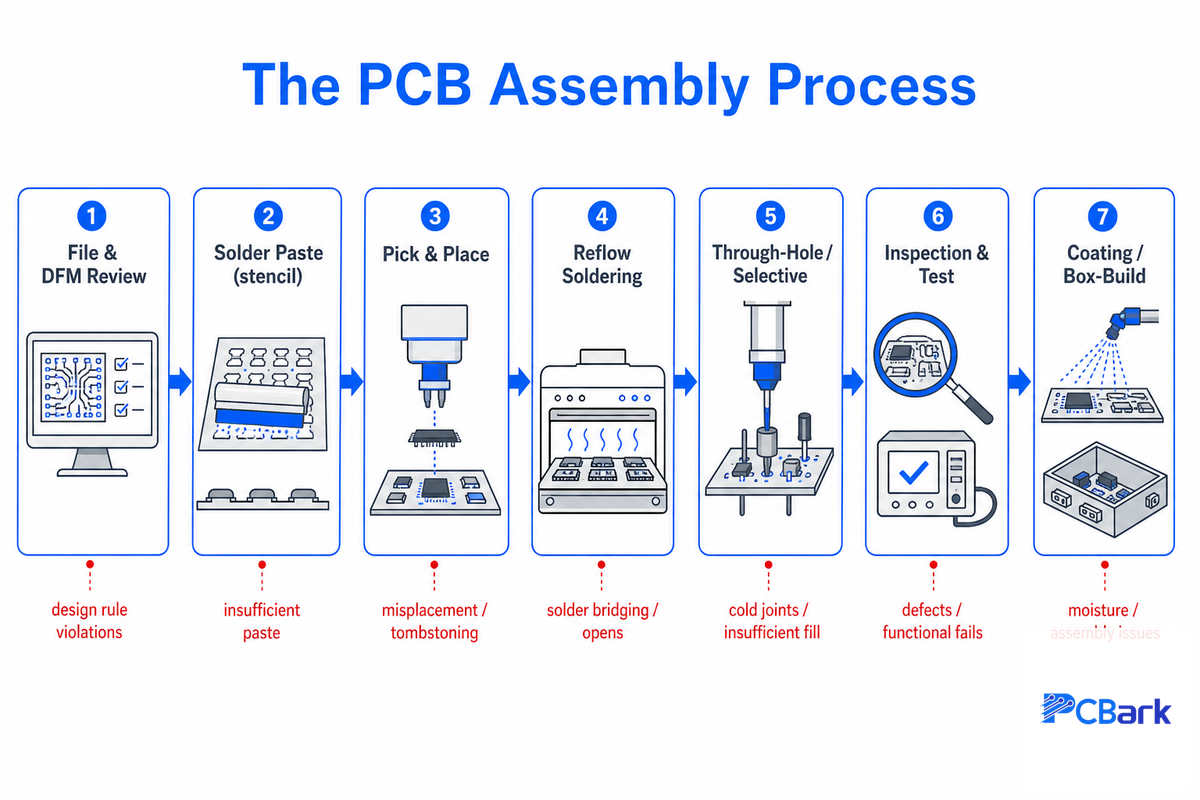
Modern PCBA is a controlled, mostly automated line. Exact steps vary by board, an SMT-only board skips the through-hole stage, while a finished product may add box-build, but the backbone is the six to seven stages below. One column most guides skip is the last: what goes wrong at each stage.
| Stage | What happens | What can go wrong |
|---|---|---|
| 1. File & DFM review | Gerber, BOM, and centroid are checked for manufacturability before any board is touched. | Missing files, unclear polarity, obsolete parts — the top cause of stalled quotes. |
| 2. Solder paste | A laser-cut stencil (typically 4–6 mil) deposits solder paste onto each SMT pad. | Too much paste bridges; too little starves the joint. |
| 3. Pick & place | A high-speed pick-and-place machine handles component placement onto the wet paste, guided by the centroid file and board fiducials. | Wrong part, wrong rotation, or shift if fiducials are missing. |
| 4. Reflow soldering | A reflow oven runs a preheat–soak–reflow–cool profile that melts the paste into solid joints. | A wrong thermal profile causes tombstoning, voids, or cold joints. |
| 5. Through-hole / selective | Connectors and large parts are inserted, then wave-soldered (~260 °C / 500 °F) or selective-soldered. | Bridging or insufficient fill on dense connector rows. |
| 6. Inspection & test | AOI, X-ray (for hidden joints), and electrical test verify the build. | Escapes if the test stack does not match the board’s complexity. |
| 7. Coating / box-build | Optional conformal coating, cleaning, and final (box-build) assembly. | Coating over connectors; trapped flux residue under parts. |
Process backbone follows IPC J-STD-001 soldering practice; stage list adapted from production-line references.
Together, these process steps turn a bare board into a finished, assembled board: the PCBA process places SMT parts and surface-mount device packages onto boards with components on one or both sides, combining SMT and through-hole work wherever a design needs both.
Step 2 deserves a note on materials. Most boards use lead-free, RoHS-compliant solder paste, a typical SAC alloy runs about 96.5% tin, 3% silver, 0.5% copper, printed through a 4–6 mil (0.1–0.15 mm) stencil and reflowed to a peak near 245 °C (480 °F). Leaded paste is still used in some legacy and high-reliability builds. Mixing leaded and lead-free parts in a RoHS build is a classic error, and tin-rich finishes raise tin-whisker questions on long-life hardware, flag your compliance target on the BOM. For the soldering acceptance rules behind every joint, see IPC J-STD-001 and its Space Addendumthe high-reliability version that NASA’s technical standards now point to. Boards built mostly on the surface-mount line are covered in depth in our SMT assembly overview.
What is the difference between PCB fabrication and PCB assembly?
Fabrication makes the bare board; assembly populates it. They’re usually two different production lines, sometimes two different suppliers. Traditional PCB assembly starts with bare printed circuit boards, the PCB boards from fabrication, before any assembly work or downstream manufacturing services begin. A “fab + assembly” or full PCB assembly service handles both under one roof, which removes the hand-off gap where fabrication tolerances and assembly footprints can disagree.
SMT vs. Through-Hole vs. Mixed Assembly
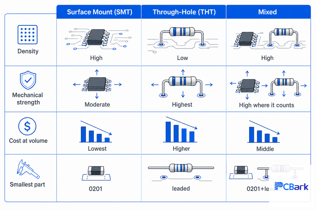
Most boards don’t get to “pick” a method, the components decide. Fine-pitch ICs and passives are surface-mount; high-stress connectors and some power parts are through-hole. A pick and place machine sets these tiny parts, down to 0201 (0.6 × 0.3 mm) and 01005 (0.4 × 0.2 mm) — at speed and roughly ±0.05 mm accuracy, which is one reason high-volume boards favour surface mount. What you decide is which dominates and whether you need both, including any thru-hole components that change the line.
✔ Surface mount (SMT)
- High density, both sides of the board
- Lowest cost at volume (automated)
- Required for fine-pitch and 0201/01005 parts
⚠ Through-hole (THT)
- Strongest mechanical bond (load-bearing connectors)
- Slower, more hand or selective soldering
- Eats board space; harder to automate
| Factor | SMT | Through-hole | Mixed |
|---|---|---|---|
| Density | Highest | Low | High |
| Mechanical strength | Moderate | Highest | High where it counts |
| Cost at volume | Lowest | Higher (labor) | Middle |
| Typical parts | ICs, passives, BGAs | Connectors, transformers | Both |
| Smallest part | 0201 / 01005 | Leaded packages | 0201 + leaded |
Method definitions per surface-mount technology; placement and reliability research is published through IEEE.
💡 The SMT-or-Through-Hole Fit Test
Three signals tell you which line your board belongs on: (1) scan the BOM — if it is mostly fine-pitch SMT packages, it is an SMT board; (2) check for load-bearing connectors or parts that take mechanical stress — those force through-hole; (3) look at volume — high volume rewards SMT automation. Most real products land on a mixed line.
Design Files & DFM: What to Get Right Before Assembly
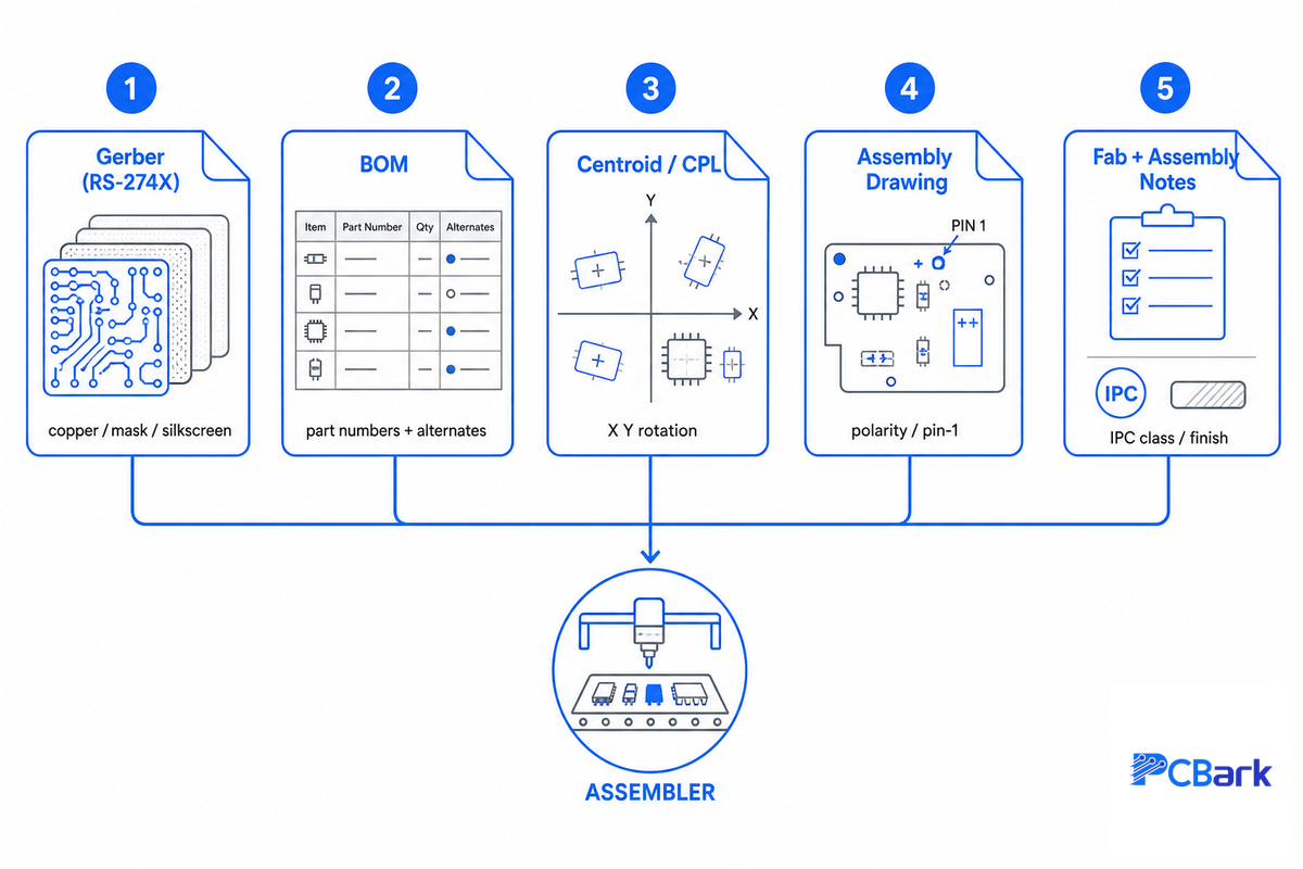
By far the biggest source of delay isn’t the line, it’s an incomplete file package. Get the hand-off right and a quote move; get it wrong and your board waits. Good PCB design carries through to a clean handoff, so here’s the set every assembler needs.
| File | What it carries | Common gap |
|---|---|---|
| 1. Gerber (RS-274X) | Copper, solder mask, silkscreen, board outline. | Missing layers or outline; no paste layer for the stencil. |
| 2. Bill of Materials (BOM) | Every part, with manufacturer part number and approved alternates. | Generic descriptions, no MPN, no “substitute allowed?” column. |
| 3. Centroid / CPL | X/Y position and rotation of each part (pick-and-place file). | Wrong origin or rotation reference — every part lands turned. |
| 4. Assembly drawing | Polarity, pin-1 marks, special orientation notes. | No polarity reference for diodes, ICs, electrolytics. |
| 5. Fab & assembly notes | Class target, finish, panelization, test points, coating. | No IPC class stated; no fiducials or tooling rails for the line. |
File set compiled from production DFM practice; see Gerber format, with design-for-manufacturing research from NIST.
A note on the future of the hand-off: the IPC-2581 format is gaining ground as a single file that carries what Gerber leaves out, stackup, materials, netlist, and design intent. It isn’t a replacement yet; Gerber plus the BOM and centroid remains the standard package, and many assemblers still receive Gerber on the vast majority of jobs. Treat IPC-2581 as an option that reduces back-and-forth on complex boards, not as a requirement.
📐 Engineering Note
DFM issues that most often delay a build are mechanical, not exotic: insufficient annular ring, parts placed too close for the nozzle or for AOI (tight spacing creates inspection shadows), missing fiducials, and components not supplied in tape-and-reel. Add tooling rails for the conveyor and keep a 3–5 mm component keep-out from the board edge.
Quality Standards Decoded: IPC-A-610 Class 1, 2 & 3
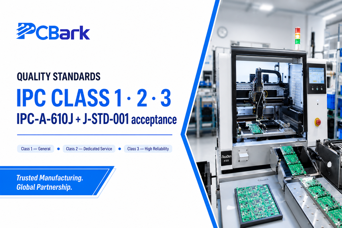
Two standards govern most assembly work. IPC J-STD-001 (currently the 2024 “J” revision) sets the soldering process requirements; IPC-A-610J (2024) sets the acceptance criteria you inspect against. Within IPC-A-610 there are three classes, and choosing the right one is a cost decision as much as a quality one.
| Class | Name / end-use | Acceptance strictness | Examples |
|---|---|---|---|
| Class 1 | General Electronic Products | Functional acceptance; cosmetic latitude | Toys, low-cost consumer goods |
| Class 2 | Dedicated Service Products | Reliable service; limited defects allowed | Most industrial, commercial, and consumer electronics |
| Class 3 | High-Reliability / High-Performance | Strictest — near-perfect registration, tighter annular ring | Medical, aerospace, defense, automotive safety |
Class definitions per IPC-A-610J (2024); high-reliability soldering follows the J-STD-001 Space Addendum that NASA adopted in place of its retired NASA-STD-8739.2/.3.
⚠️ The IPC Class Reality Check
Higher is not automatically better. Specifying Class 3 on a consumer board raises cost without buying you reliability you need — and industry working groups note that even Class 3 standards are “not always sufficient or appropriate” for the harshest environments, where extra qualification beyond the class is what matters. Match the class to the end-use: Class 2 covers most industrial and commercial work; reserve Class 3 PCB assemblies for hardware where a field failure has safety or mission cost.
Inspection & Testing: How Defects Are Caught
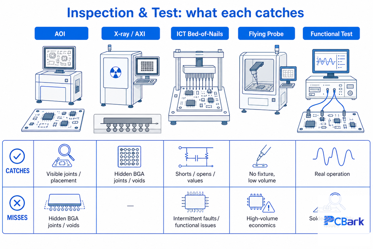
No single method catches everything. A board with BGAs needs X-ray; a high-mix board need flying probe; a high-volume board earns a test fixture. Your test stack should match the board’s complexity and class, complex PCB assemblies need more than AOI alone.
| Method | Catches | Misses | Use when |
|---|---|---|---|
| AOI (optical) | Visible joints, polarity, missing/shifted parts | Hidden joints under BGAs | Every board |
| X-ray (AXI) | BGA/QFN joints, voids, head-in-pillow | Electrical function | Any board with BGAs or bottom-terminated parts |
| ICT (in-circuit) | Shorts, opens, wrong values (bed-of-nails) | Firmware/system behavior | Higher volume (fixture cost amortizes) |
| Flying probe | Shorts, opens, values — no fixture | Speed (slower than ICT) | Prototype and low volume |
| Functional (FCT) | Real operating behavior | Root cause of a failure | Final sign-off |
See automated optical inspection. Recent patents (for example adaptive radioscopic inspection, EP4134883B1) add machine-learning defect calls on top of these methods.
Common PCBA Defects and Their Root Causes
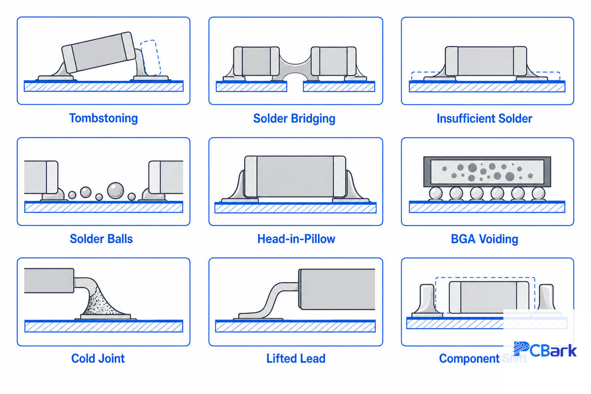
Most solder defects trace back to a small number of causes, paste, profile, pad design, or placement. Use this table as a triage tool: find the defect, read across to the cause, the fix, and how it’s caught. Many defects on PCB assemblies are prevented at the design stage, not on the line.
The 10-Row Defect-to-Cause Map
| Defect Type | Root cause | Prevention | Caught by |
|---|---|---|---|
| Tombstoning | Uneven pad heating / paste | Balanced pads, tuned reflow ramp | AOI |
| Solder bridging | Excess paste, fine pitch | Stencil aperture reduction, solder mask | AOI / AXI |
| Insufficient solder | Low paste volume, oxidation | Stencil thickness, nitrogen reflow | AOI |
| Solder balls | Paste slump, fast ramp | Profile soak control | AOI |
| Head-in-pillow | Warped BGA, oxidation | Profile + fresh paste, ball coplanarity | X-ray |
| BGA voiding | Outgassing, via-in-pad | Filled/capped vias, profile | X-ray |
| Cold joint | Peak temp too low | Validated thermal profile | AOI / FCT |
| Lifted lead / open | Coplanarity, placement | Inspect incoming coplanarity | X-ray / ICT |
| Component shift | Placement accuracy, paste flow | Fiducials, placement calibration | AOI |
| Flux residue | Incomplete cleaning | No-clean paste or validated wash | Visual / cleanliness test |
Acceptance limits per IPC-A-610J; high-reliability fillet rules per the J-STD-001 Space Addendum that NASA’s workmanship standards reference.
When do you need conformal coating?
Conformal coating protects a finished board from humidity, dust, salt fog, and condensation. Acrylic is easy to apply and rework; silicone tolerates heat and flex; urethane resists chemicals; parylene gives the thinnest, most uniform film for medical and aerospace. If your product lives outdoors, in a vehicle, or near moisture, plan coating, and define keep-out zones around connectors and test points in the assembly drawing so they aren’t coated shut.
On a full PCB project, the coating process is followed by mechanical assembly and final assembly, fitting the enclosure and cabling into the finished unit.
“In our DFM reviews, the defects customers blame on the line are usually designed in, unbalanced pads that tombstone, vias in pads that void, or parts spaced so tightly that AOI cannot see between them. The cheapest defect is the one caught in the file review, not on the board.”
PCBark technical team
Turnkey vs. Consigned Assembly: The Sourcing Decision
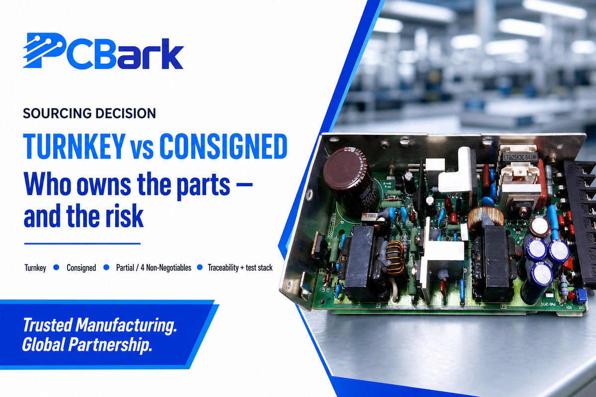
Once the board is designed, you choose who owns the parts. These three models trade control for convenience, and the choice also shape any box-build assembly that follows.
| Model | Who sources parts | Best for |
|---|---|---|
| Turnkey | Assembler sources everything | Most buyers; fastest, one point of accountability |
| Consigned | You supply all parts | Tight control of specific parts or allocation |
| Partial turnkey | Assembler sources common parts; you supply criticals | Long-lead or controlled components |
A full prototype PCB assembly run is usually turnkey; production may shift to partial as you lock long-lead parts.
Vetting starts with reading an assembler’s assembly capabilities, not its homepage. A trusted PCB assembly partner, acting as your manufacturing partner for both prototype and volume production, should show real PCB assembly capabilities across printed circuit board assembly services, from small volume runs to volume PCB assembly, scaling from prototype to production. Not all PCB assembly manufacturers work this way: a PCB assembly company that keeps assembly and testing under one roof, from circuit assembly through final electronic assembly, removes the hand-offs that a thinner electronic manufacturing services shop can’t.
The Four Non-Negotiables for Vetting an Assembler
- IPC class capabilitycan they build and inspect to your class (1/2/3), with certified operators?
- ISO 9001a real, current quality-management certificate, not a logo.
- Traceability & sourcing integritylot/date-code traceability and authorized-channel component sourcing, so counterfeit or out-of-spec parts are screened out (the risk rise with allocation and long-lead parts).
- In-house test stackAOI, X-ray, and electrical test under one roof, not subcontracted.
A note from the field: the most common reason buyers move from in-house to outsourced assembly isn’t capability but logistics, keeping the parts inventory stocked to feed a pick-and-place line is its own full-time job. A high-quality partner absorbs that, and screens incoming parts as it does.
What Drives PCB Assembly Cost and Lead Time
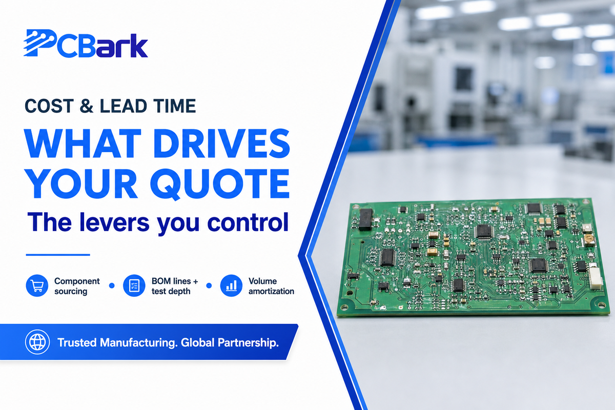
There’s no single PCB assembly price, the same board can quote very differently depending on choices you control. Your quote reflects the PCB assembly parts you specify as much as the board itself, so rather than a price list (which goes stale fast), here are the levers.
Cost drivers (the ones you control)
- Component sourcing and availability, allocation and long-lead parts dominate both cost and schedule.
- BOM line count, more unique parts means more setup, not just more parts.
- SMT-to-through-hole mix, hand and wave soldering of through-hole components add labor.
- Test depth, functional test and fixtures cost more than AOI alone.
- Volume, at 100–500 boards, setup isn’t yet amortized, so per-board cost stays high; it drops as quantity rises.
- Panelization and finish, efficient panel use and a standard finish cut both cost and yield risk.
Lead time follows the same logic: the gating item is almost always component lead time, then stencil and first-article approval, manufacturing-cost research from NIST points to setup and changeover as the dominant fixed cost at low volume. Your fastest route to a quicker, cheaper quote is a clean PCB assembly file package and an early BOM review so part substitutions are agreed before the build, not during it.
The 2026 Outlook: What’s Changing in PCB Assembly
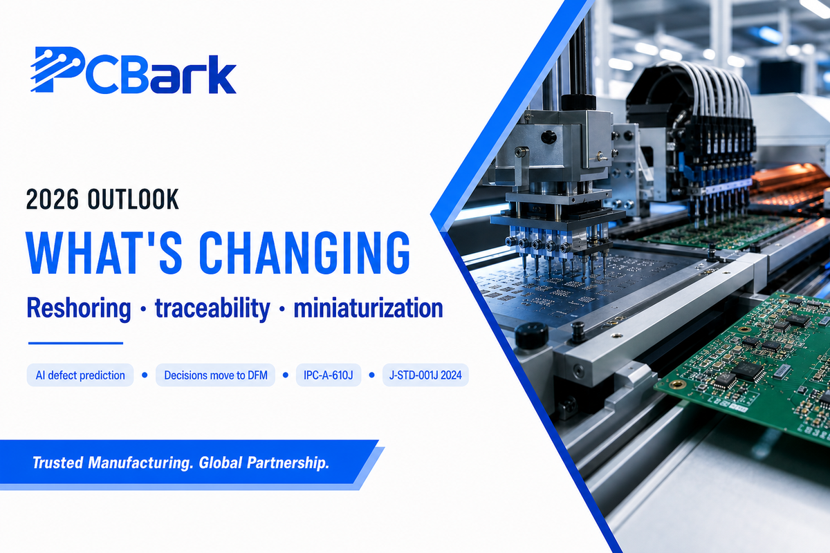
What’s actually shifting isn’t market size, it’s where the build decision happens. Reshoring, tighter component-traceability expectations, and relentless miniaturization (0201, 01005, and finer-pitch BGAs) are pushing manufacturability decisions earlier, into the design and DFM stage. What you can actually build at Class 2 or 3 is increasingly decided before the layout is finished, not after.
Two concrete movements back this up. First, automation is moving from “place faster” to “predict defects”: granted patents now describe machine-learning tools that fuse process data to flag quality risk before inspection (for example an SMT process-prediction tool, US11825606B2), which raises first-pass yield across high-volume PCB assemblies. Second, standards refreshed, IPC-A-610 and J-STD-001 both moved to their “J” revisions in 2024, so an assembler who still cites an unnamed revision is a freshness flag worth questioning.
For buyers, the action item is simple: design for your class from the start, send a complete file package, and pick a partner whose process and standards are current. Market context, PCB assembly remains the largest slice of a growing electronics-manufacturing-services sector, is real but secondary to those choices.
Frequently Asked Questions
What is PCB assembly, and what does PCBA stand for?
View Answer
PCBA stands for printed circuit board assembly. It is the process of soldering electronic components — resistors, capacitors, ICs, connectors — onto a bare, fabricated printed circuit board so the design becomes a working electronic board. That same acronym also names the finished, populated board. It is the stage after PCB fabrication, which makes the blank board itself.
What is the difference between PCB fabrication and PCB assembly?
View Answer
PCB fabrication (also called PCB manufacturing) builds the bare board from copper-clad laminate: the etched traces, drilled holes, solder mask, and silkscreen. PCB assembly then mounts and solders the components onto that board. They are usually separate production lines and can be separate suppliers; a turnkey service runs both, which removes the hand-off gap between fabrication tolerances and assembly footprints.
How much does PCB assembly cost?
View Answer
There is no flat rate — cost is driven by component sourcing, the number of unique BOM lines, the SMT-versus-through-hole mix, how deep the testing goes, and volume. Setup cost is fixed, so at low quantities (roughly 100–500 boards) the per-board price stays high and then falls as volume amortizes it. The most reliable way to lower a quote is a complete file package and an early BOM review, so part substitutions are settled before the build.
How long does PCB assembly take?
View Answer
Prototype assembly is typically 1–3 weeks; production runs longer. The gating item is almost always component lead time, not the line itself.
Do I need SMT or through-hole assembly?
View Answer
The components decide. Fine-pitch ICs and small passives are surface-mount; load-bearing connectors and some power parts are through-hole. Scan your BOM: if it is mostly SMT packages, you are on an SMT line; if you have stressed connectors, you need through-hole too. Most real boards are a mix of both.
What files do I need to provide for PCB assembly?
View Answer
Five: Gerber files (copper, mask, silkscreen, outline), a Bill of Materials with manufacturer part numbers and approved alternates, a centroid/pick-and-place file with X/Y and rotation, an assembly drawing showing polarity and pin-1, and fab/assembly notes stating your IPC class, finish, and any test or coating requirements. On complex boards, an IPC-2581 file can carry stackup and netlist data that Gerber omits, but Gerber plus the BOM and centroid remains the standard package.
Is “PCB” the same as the banned chemical?
View Answer
No. In electronics, PCB means printed circuit board. That banned “PCB” is polychlorinated biphenyl, an unrelated industrial chemical.
Related Reading
- PCB assembly servicesfull turnkey, SMT, through-hole, and box-build under one roof
- SMT assemblythe surface-mount line in detail
- Prototype PCB assemblyquick-turn, low-volume builds
- PCB manufacturing and fabricationthe bare-board step before assembly
About This Guide
This guide draws on PCB assembly practice across eight surface-mount lines running up to nine million placements per day, down to 0201 parts, with in-house AOI, 3D X-ray, in-circuit, flying-probe, and functional test, built to IPC-A-610 Class 2 and Class 3 and J-STD-001. Where we cite numbers, we cite the standard or source; where a figure depend on your board, we say so rather than invent a value. Reviewed by the Shenzhen Linghangda Technology (PCBark) technical team.
References & Sources
- IPC-A-610J (2024), Acceptability of Electronic AssembliesIPC, via ANSI
- IPC J-STD-001 and the Space Hardware AddendumIPC / Global Electronics Association
- NASA Technical StandardsNASA (adopted the J-STD-001 Space Addendum in place of NASA-STD-8739.2/.3)
- IPC-2581 Consortiumdigital product model data exchange
- ISO 9001 Quality ManagementInternational Organization for Standardization
- US11825606B2, SMT process prediction tool for PCB qualityUSPTO via Google Patents