Get in touch with PCBark Company

Decoupling Capacitor Guide: Bypass Capacitor Circuit Role, Value Calculation & PCB Layout Rules

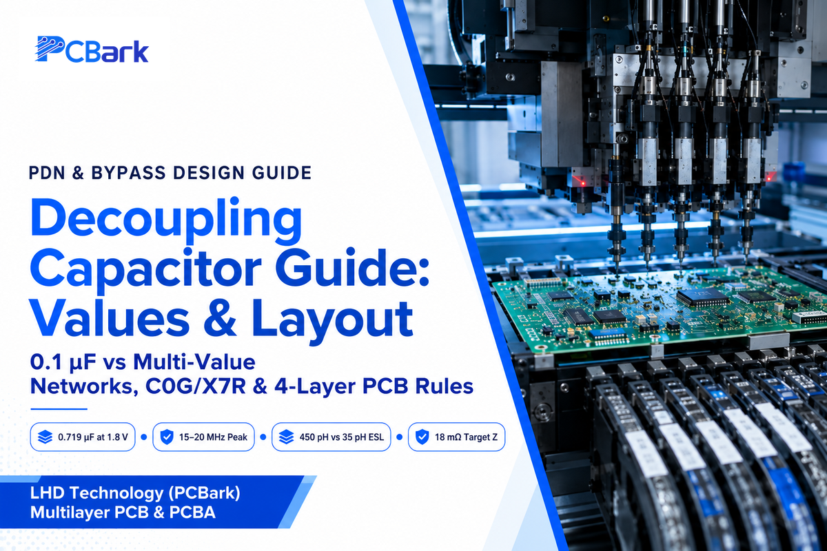
Key Engineering Takeaways:
- Dual Circuit Function: A decoupling capacitor serves as a local charge reservoir for fast load steps. It also provides a low-impedance AC shunt to ground.
- Effective Capacitance Reality: Per Analog Devices’ benchmark, a 1 μF, 10 V X5R 0402 capacitor retains 0.719 μF at 1.8 V DC bias. That figure includes voltage, temperature, and tolerance derating.
- Parallel Anti-Resonance Risk: Connecting low-ESR ceramic capacitors with values like 10 μF and 100 nF in parallel creates a parallel LC tank between their self-resonant frequencies. Mounting inductance shifts the peak frequency, and losses limit its height.
- Layout Dominates Inductance: Standard 0603 MLCCs have 450 pH of internal ESL. However, PCB traces add about 1 nH/mm, unless routed with close side-via pairs or via-in-pad (VIPPO).
In precision digital circuits and high speed analog circuits, a decoupling capacitor stabilizes the power supply line on the printed circuit board. Supplying local transient current is the primary function of a decoupling capacitor alongside noise decoupling to ground. Placing the part near the active IC pin preserves signal integrity across neighboring traces. The decoupling capacitor’s local charge reservoir prevents collapse of the rail across regulated power supplies when a fast capacitor is used adjacent to a logic gate.
Analog Devices’ LDO bypass engineering study shows that a 1 μF, 10 V X5R 0402 capacitor drops to 0.719 μF of effective capacitance at 1.8 V DC bias. Meanwhile, NextPCB’s PDN hierarchy analysis notes a 15–20 MHz parallel anti-resonance peak when pairing 10 μF and 100 nF MLCCs. Mounting inductance and circuit losses govern the exact peak frequency and height. Below, we examine the series RLC model, dielectric derating, target impedance math, and 4-layer via placement rules.
What Does a Decoupling Capacitor Do in Electronic Circuits and How Does It Stop Voltage Droop?
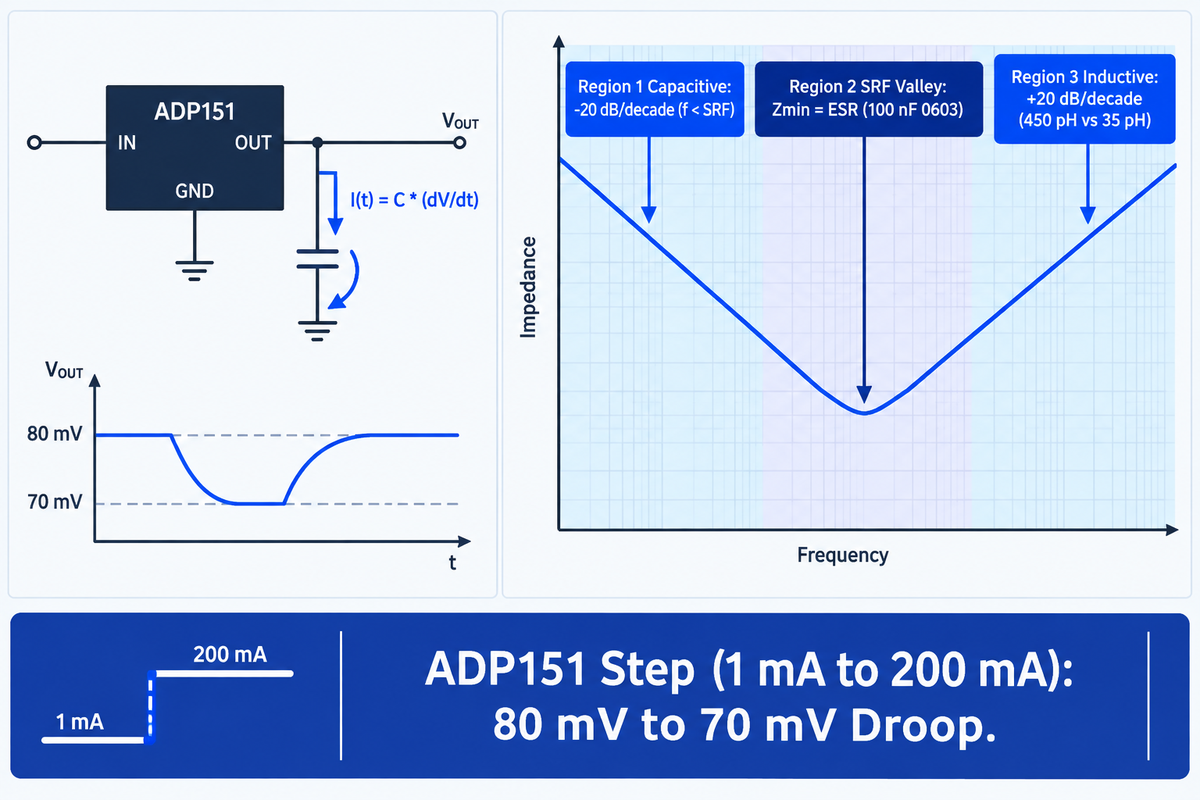
A decoupling capacitor is a passive shunt component placed across an integrated circuit’s power and ground pins to provide transient current and suppress voltage droop. It isolates fast switching loads from the upstream power distribution (PDN) network and provides a low-impedance path for high frequency switching noise.
How does a decoupling capacitor work?
A decoupling capacitor discharges stored electrostatic energy during nanosecond load steps and shunts AC ripple to ground via a low equivalent series resistance path. When an IC switches state, its current draw rises quickly (steep slew rate: dI/dt). Because every copper trace and via has a certain inductance, this rapid change induces a transient voltage drop governed by Faraday’s law.
Transient Voltage Droop Equation: ΔV = L ⋅ (dI / dt) | Capacitive Charge Delivery: I(t) = C ⋅ (dV / dt)
When a load step increases more quickly than a remote regulator and its interconnect can deliver additional current, local capacitance supplies the initial current deficit. Bulk reservoirs handle low-frequency decoupling during millisecond load transitions. Compact ceramic capacitors cover the megahertz-to-gigahertz frequency range and stabilize the local power supply voltage. In the Analog Devices test on the ADP151 regulator, a 1 mA to 200 mA step at 500 mA/μs caused an 80 mV droop with a 1 μF capacitor. Increasing that local capacitor from 1 μF to 10 μF reduced the transient voltage droop from 80 mV to 70 mV.
No physical capacitor exhibits ideal behavior across all frequencies. As described by the European Passive Components Institute (EPCI / KYOCERA AVX), every multilayer ceramic capacitor (MLCC) acts like a series RLC network. This network contains effective capacitance (C), equivalent series resistance (ESR), and equivalent series inductance (ESL):
Series RLC Impedance Magnitude: |Z(f)| = √[ ESR2 + (2πf · ESL − 1 / (2πf · C))2 ]
Our 3-Region MLCC Impedance-Frequency Model captures this behavior in three different operating zones across frequency:
| Impedance Region | Dominant Parameter | Reactance & Slope Behavior | Primary PDN Engineering Role |
|---|---|---|---|
| Region 1: Capacitive Reservoir Zone (f < SRF) | Effective Capacitance (CEFF) | XC = 1 / (2πfCEFF); impedance falls at −20 dB/decade | Supplies local electrostatic charge to limit transient voltage droop during fast load steps |
| Region 2: Self-Resonant Valley (f = SRF) | Equivalent Series Resistance (ESR) | XC = XL; Zmin = ESR at resonant crossover point (100 nF, 0603 MLCC per EPCI) | Delivers lowest possible shunt impedance to ground at the resonant frequency |
| Region 3: Inductive Skirt Zone (f > SRF) | Total Loop Inductance (ESL + Lmount) | XL = 2πf(ESL + Lmount); impedance climbs at +20 dB/decade | Governed by package geometry (450 pH on 0603 vs 35 pH on 0306 IDC) and via loop area |
Decoupling vs. Bypass Capacitor: Comparing Decoupling and Bypass, Coupling, and Bulk Roles
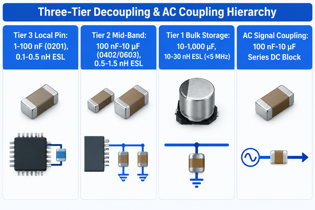
In modern circuit design, bypass and decoupling capacitors stabilize power distribution networks, while a series coupling capacitor is engineered to pass AC while blocking DC bias.
A bypass capacitor shunts high-frequency supply noise directly to the ground plane. A decoupling capacitor buffers local transient current so that switching spikes don’t disturb other sub-circuits sharing the same rail.
Are bypass and decoupling capacitors the same?
Bypass and decoupling capacitors often use the exact same physical MLCC component on a BOM, but their circuit roles describe different aspects of power integrity. Bypassing refers to shunting AC noise to ground, while decoupling refers to isolating transient current pulses between stages. To coordinate these roles across six decades of frequency, NextPCB’s three-tier decoupling framework divides board capacitance into three tiers. Tier 1 bulk capacitors sit near the regulator output or board entry and span 10–1,000 μF with 10–30 nH ESL, placing their series RLC resonances below 5 MHz. Tier 2 mid-frequency decoupling uses 100 nF–10 μF parts in 0402 or 0603 packages along the sub-rail distribution path. With 0.5–1.5 nH ESL, the series RLC model places their self-resonant frequencies below 30 MHz. Tier 3 high-frequency decoupling can use 1–100 nF capacitors in 0201 packages mounted directly at IC pins. Low-nF parts reach 150–500 MHz, while a 100 nF capacitor with 0.1–0.5 nH ESL resonates below 150 MHz.
| Capacitor Role | Circuit Topology | Typical Value & Package | Parasitic ESL & Resonant Behavior | Core Electrical Objective |
|---|---|---|---|---|
| Tier 3 Local Pin Decoupling Capacitor | Shunt from IC supply pin to local ground | 1–100 nF (0201 C0G/X7R MLCC) | 0.1–0.5 nH ESL; 150–500 MHz on low-nF parts (100 nF resonates below 150 MHz) | Supply sub-nanosecond edge current and close the high-frequency return loop |
| Tier 2 Mid-Band Bypass / Decoupling Cap | Shunt from sub-rail or IC pin to ground plane | 100 nF–10 μF (0402/0603 X7R/X5R MLCC) | 0.5–1.5 nH ESL; series RLC resonances fall below 30 MHz (NextPCB 30–80 MHz tier) | Shunt mid-band conducted noise and bridge VRM response delay |
| Tier 1 Bulk Energy Storage Capacitor | Shunt at VRM output or board power entry | 10–1,000 μF in NextPCB’s Tier 1 model | 10–30 nH ESL in NextPCB’s Tier 1 model; series RLC resonances fall below 5 MHz | Buffer low-frequency load steps and provide ESR damping when matched to network impedance |
| AC Signal Coupling (DC Blocking) Capacitor | Series in-line along high-speed or audio signal trace | 100 nF–10 μF (C0G or low-distortion X7R) | Low insertion loss across signal passband | Transmit AC signal swing while isolating DC bias levels between stages |
While reading polarized and non-polarized capacitor schematic symbols, non-polarized ceramic decoupling capacitors show a pair of parallel straight lines. Polarized electrolytic and tantalum capacitors have a straight anode plate with a curved cathode plate and show a plus (+) near the power entry point.
Why 0.1 μF (100 nF) Became the Default Rule of Thumb, and When Target Impedance Needs Multi-Value Networks
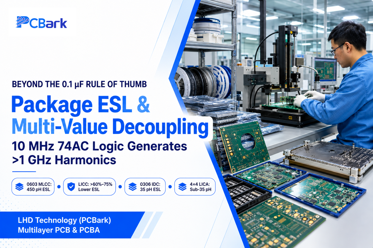
The 0.1 μF (100 nF) ceramic capacitor became a traditional rule of thumb because it buffered switching transients in legacy logic families. Switches in current multi-rail processors still buffer the switching transients, and the edges may be far faster than a nanosecond. On modern multi-rail processors with sub-nanosecond edges, engineers replace single-value habits with multi-value 0402 and 0201 networks. Such networks must simultaneously satisfy anti-resonance, DC-bias derating, mounted inductance, and target impedance bandwidth constraints.
EDN’s AVX analysis challenges the single 0.1-μF capacitor rule for modern multi-rail ICs. Above self-resonance fSRF = 1 / (2π√(ESL · C)), the capacitor becomes inductive, yet it can still provide useful decoupling while the installed power-distribution impedance remains below the target. Harmonic bandwidth tracks logic edge rate rather than clock frequency. As practitioners on the EEVblog forum note, even a 10 MHz clock on a 74AC logic IC generates sub-nanosecond edges with harmonics above 1 GHz.
Well above self-resonance, designers can lower inductive reactance by reducing package and mounting inductance through smaller values in compact 0201 packages, low-inductance geometries, or shorter current loops. Reducing capacitance alone doesn’t decrease inductive reactance. Anti-resonance can also be caused by paralleling capacitors with different values. Per AVX data in EDN and KYOCERA AVX (EPCI), a standard 0603 MLCC exhibits 450 pH of internal ESL. Reverse-geometry Low-Inductance Chip Capacitors (LICC) decrease ESL by more than 60% to 75%. An 8-terminal 0306 Interdigitated Capacitor (IDC) shows an ESL of 35 pH, which is almost 70% lower than that of a 0306 LICC.
| Capacitor Type & Decoupling Tier | EIA Package & Value Range | Equivalent Series Inductance (ESL) | Resonant & High-Frequency Behavior | Verified Source Benchmark |
|---|---|---|---|---|
| Tier 1 Aluminum Electrolytic Capacitor | Radial / SMD Can (10–1,000 μF) | 10–30 nH ESL in NextPCB’s Tier 1 model | Series RLC resonances fall below 5 MHz | NextPCB 3-Tier Strategy |
| Tier 1 Conductive Polymer Tantalum | Molded SMD Chip (10–1,000 μF) | Controlled milliohm ESR; bulk package ESL | Buffers low-frequency load steps and damps PDN ringing when ESR matches network impedance | Analog Devices & NextPCB |
| Tier 1 Large Bulk Ceramic MLCC | 0805–1210 X5R/X7R (10–100 μF) | Low ESR; requires DC-bias derating | 100 μF 6.3 V X5R yields 30–50 μF at 3.3 V DC bias | NextPCB Bulk Strategy |
| Tier 2 Standard Mid-Band MLCC | 0603 X7R/X5R (100 nF–10 μF) | 450 pH bare-body ESL; 0.5–1.5 nH mounted | Series RLC resonances fall below 30 MHz for 0.5–1.5 nH ESL | EDN (AVX) & NextPCB |
| Tier 2 Compact Mid-Band MLCC | 0402 X7R/X5R (100 nF–1 μF) | 0.5–1.5 nH mounted ESL | 1 μF 10 V X5R retains 0.719 μF CEFF at 1.8 V bias after temperature and tolerance | Analog Devices & NextPCB |
| Tier 3 Ultra-Small Local Pin MLCC | 0201 C0G/X7R (1–100 nF) | 0.1–0.5 nH ESL | 150–500 MHz tier on low-nF values (100 nF resonates below 150 MHz) | NextPCB 3-Tier Strategy |
| Reverse-Geometry Low-Inductance MLCC (LICC) | 0306 / 0508 Wide-Terminal | >60% to >75% ESL reduction vs 0603 | Pushes inductive reactance skirt to higher frequencies | EDN (AVX) & KYOCERA AVX (EPCI) |
| 8-Terminal Interdigitated Capacitor (IDC) | 0306 8-Terminal Package | 35 pH ESL (~70% below 0306 LICC; down from 450 pH on 0603) | Opposing internal currents cancel magnetic flux on BGA rails | EDN (AVX) |
| Low-Inductance Chip Array (LICA) | 4×4 C4 Solder-Bump Array | Sub-35 pH flip-chip vertical termination | Direct BGA package and high-speed processor core decoupling | EDN (AVX) |
Choosing the Right Capacitor for Decoupling: Ceramic Capacitors (C0G, X7R) vs. Electrolytic and Tantalum
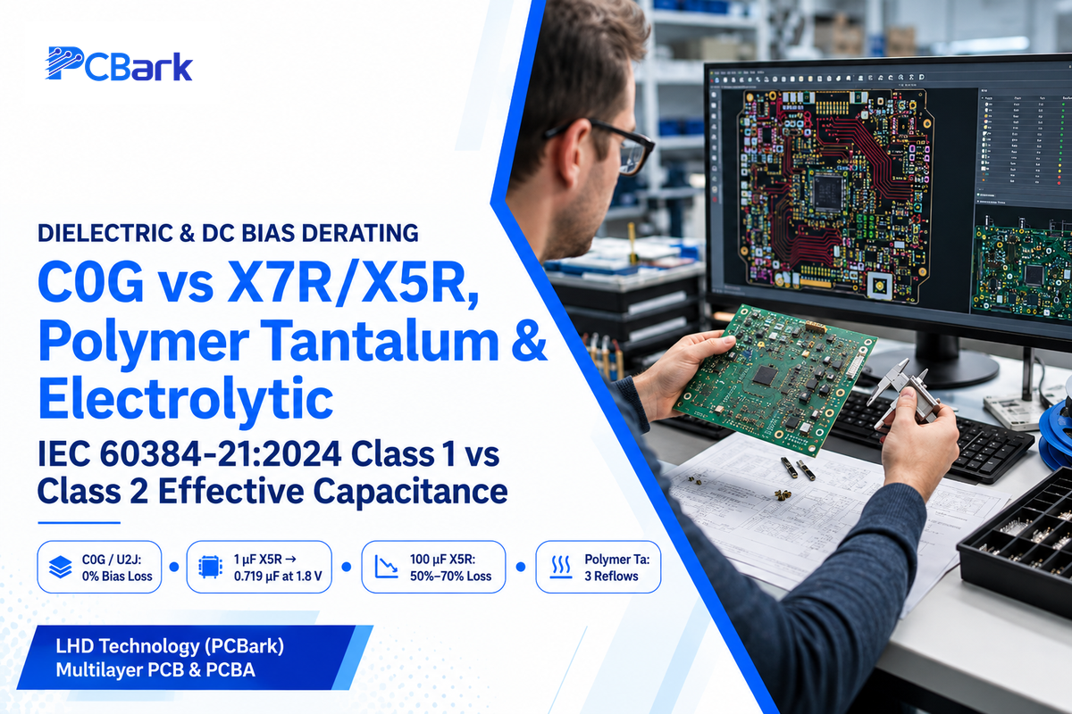
Use multilayer ceramic capacitors (MLCCs) for high-frequency local decoupling and electrolytic or polymer tantalum capacitors for bulk energy storage, selecting the dielectric class based on voltage bias, temperature and acoustic limits. Each type of capacitor balances dielectric stability, equivalent series resistance, and volumetric efficiency across decoupling applications. In IEC 60384-21:2024 Edition 4.0, Class 1 SMC MLCCs (such as C0G/NP0 and U2J) offer linear capacitance with zero DC bias loss. Class 2 ferroelectric dielectrics (X7R and X5R) can achieve higher capacitance in smaller packages. However, they require vendor DC-bias curves for precise in-circuit derating.
As Analog Devices shows, the actual in-circuit effective capacitance (CEFF) of a Class 2 MLCC must be assessed with consideration to tolerance, temperature and DC bias:
Effective Capacitance Equation: CEFF = CBIAS × (1 − TVAR) × (1 − TOL)
Consider Analog Devices’ benchmark example. A nominal 1 μF, 10 V X5R 0402 capacitor operating at 1.8 V DC bias drops to 0.94 μF. Accounting for ±15% temperature variation (−40 °C to +85 °C in that application example) and ±10% tolerance reduces effective capacitance CEFF to 0.719 μF. In tighter packages, derating is even steeper. NextPCB notes that a 100 μF, 6.3 V X5R MLCC can lose 50% to 70% of its capacitance at 3.3 V DC bias, delivering only 30–50 μF. Analog Devices also notes that Class II MLCCs exhibit piezoelectric microphonics on vibration-sensitive PLL or VCO rails. By contrast, polymer tantalum capacitors are free of microphonic noise and rated for up to 3 reflow solder cycles in Analog Devices’ guidelines.
| Dielectric & Manufacturer Spec | Standard & Temperature Rating | DC Bias & Effective Value Benchmark | Acoustic & Reliability Reference | Target Circuit Comparison |
|---|---|---|---|---|
| Class I Ceramic C0G / NP0 | IEC 60384-21:2024 Edition 4.0 (ultra-stable temperature coefficient) | 0% DC bias capacitance loss; ultra-low ESR | Zero piezoelectric microphonic noise | RF stages, PLLs, VCOs, precision ADC reference pins (10 pF–10 nF) |
| Class I Ceramic U2J | IEC 60384-21:2024 Edition 4.0 (defined linear temperature slope) | 0% DC bias loss; higher volumetric density than C0G | Free of ferroelectric microphonic distortion | Precision analog filters, clock buffers, and low-jitter oscillator rails |
| Class II Ceramic (X7R / X5R) | IEC 60384-22; ±15% temperature characteristic, with upper limits of +85 °C for X5R and +125 °C for X7R | Analog Devices’ 1 μF 10 V X5R 0402 example gives 0.94 μF at 1.8 V DC bias and 0.719 μF after temperature variation and tolerance are included; NextPCB reports 50–70% bias loss for its cited 100 μF 6.3 V X5R example at 3.3 V | Piezoelectric vibration sensitivity; board-flex crack risk | Digital IC pin and mid-band decoupling (100 nF–22 μF), with DC bias, temperature, and tolerance included in effective capacitance |
| Automotive AEC-Q200 Soft-Termination X7R (e.g., Murata GCJ21BD72A225KE02) | AEC-Q200 automotive qualification up to +125 °C | 2.2 μF, 100 Vdc in 0805 package cuts mounting area by 51% (Maximize Market Research) | Flexible conductive resin layer reduces depanelization flex-crack risk | 48 V automotive ADAS power rails and board-edge high-stress zones |
| Automotive High-Voltage 3225 X7R (e.g., TDK CGA & Taiyo Yuden 3225) | AEC-Q200 automotive reliability standard | TDK 10 μF 100 V 3225 X7R halves part count; Taiyo Yuden reaches 220 μF in 3225 (Maximize Market Research) | Requires symmetric land geometry and board-flex keep-out discipline | High-density 48 V automotive zone controllers and DC-DC input filtering |
| Conductive Polymer Tantalum | Polarized SMD molded chip | Stable capacitance under DC bias; controlled milliohm ESR | Zero microphonics; Analog Devices notes a 3-reflow cycle limit | Tier 1 bulk rail buffering and LDO / analog rail damping |
| Solid MnO2 Tantalum | Polarized SMD molded chip | Stable DC-bias capacitance; moderate ESR provides natural PDN damping | Zero microphonics; requires strict polarity and surge-current derating | Bulk rail damping where controlled series resistance suppresses ringing |
| Aluminum Electrolytic | Polarized radial or SMD can | High bulk energy storage (10–1,000 μF); higher ESR & ESL (10–30 nH) | Electrolyte dry-out at elevated ambient temperatures | Board power entry filtering and low-frequency (<5 MHz) energy storage |
How to Calculate the Exact Value of a Decoupling Capacitor: PDN Target Impedance Worked Example
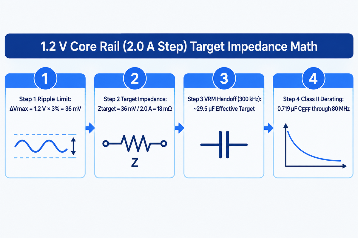
Calculate the required effective decoupling capacitance using Ceff = (ΔI × Δt) / ΔV, then determine the target impedance ceiling (Ztarget) by dividing the maximum allowable voltage ripple by the peak transient current step. The combined PDN must meet the target impedance over the specified frequency range at the chosen observation port, with board, package, and on-die decoupling covering their respective effective bands.
How do you calculate decoupling capacitor value?
A decoupling capacitor is calculated by dividing (ΔI · Δt) by the maximum allowable voltage ripple and derating for DC bias, temperature and tolerance. As formalized in USPTO Patent US10621387B2 and Missouri S&T’s 2025 IEEE EMCSIPI multi-port PDN research, the limit of dynamic power supply droop is described by two fundamental equations:
PDN Target Impedance: Ztarget = (ΔVmax) / (ΔItransient) = (VDD × Ripple%) / ΔItransient | Minimum Effective Capacitance: Cmin,eff = (ΔItransient · Δt) / ΔVmax
Board-level target impedance is evaluated at the PCB BGA ball or IC pin from the regulator handoff frequency across the active digital switching spectrum. Silicon-level droop includes the combined response of the board network, package impedance, and on-die capacitance; at high frequencies, package inductance limits the transient current that PCB capacitors can deliver to the die. Follow this 4-step worked example for a 1.2 V FPGA/MCU core rail experiencing a 2.0 A transient current step:
- Step 1, Define Maximum Allowable Voltage Ripple (ΔVmax): For a 1.2 V core supply with a ±3% ripple budget, ΔVmax = 1.2 V × 0.03 = 0.036 V (36 mV).
- Step 2: Determine Target Impedance Ceiling (Ztarget): Divide the 36 mV ripple limit by the 2.0 A transient current step. This yields Ztarget = 0.036 V / 2.0 A = 0.018 Ω (18 mΩ).
- Step 3: Estimate Effective Capacitance at VRM Handoff: Assuming a frequency of 300 kHz, an ideal capacitor would require approximately 29.5 µF to achieve a reactance of 18 mΩ. This estimate is made in the frequency domain and doesn’t account for ESR, ESL and the regulator’s transient response. A time-domain calculation accounts for the actual current deficit over the regulator response window.
- Step 4, Apply Class II Derating and Model the Mounted Network: Analog Devices’ 1 μF, 10 V X5R 0402 example yields 0.719 μF after DC bias, temperature variation, and tolerance are combined. Divide the 29.5 μF effective target by the selected 1.2 V capacitor’s verified retention factor to set nominal BOM capacitance. For the selected capacitors, effective capacitances add in parallel; their ESR, ESL, mounting inductance, and interconnections together determine whether the network meets the 18 mΩ impedance target through 80 MHz.
When Parallel Decoupling Networks Backfire: Anti-Resonance Peaks, ESL Limits, and Class II DC Bias Derating
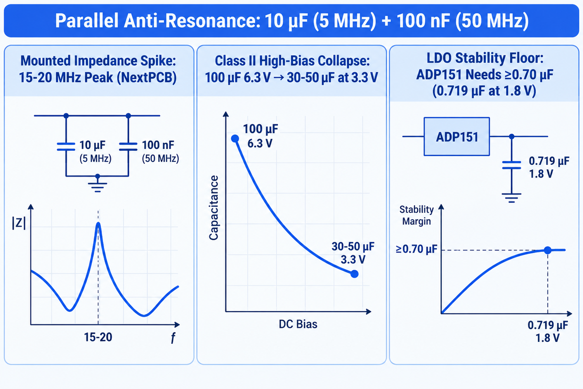
Connecting ultra-low-ESR ceramic capacitors of different values in parallel can cause a sharp impedance spike between their self-resonant frequencies. Above the larger capacitor’s self-resonant frequency, that branch acts inductively. Below the smaller capacitor’s self-resonant frequency, the other branch acts capacitively and forms a parallel LC tank circuit across power supplies.
For ideal low-loss series-RLC branches, a 10 μF capacitor with a self-resonant frequency of 5 MHz in parallel with a 100 nF capacitor resonating at 50 MHz produces an anti-resonance between those two frequencies. The 15–20 MHz peak reported by NextPCB doesn’t follow from those component parameters alone; additional mounting inductance can shift the peak downward, while circuit losses limit its height. If an IC clock harmonic falls on that peak, rail ripple amplification occurs instead of attenuation.
Regarding identical, independent series-RLC branches, KYOCERA AVX (EPCI) states that total capacitance is n·C, equivalent inductance is ESL/n, and equivalent resistance is ESR/n. The self-resonant frequency is unchanged, and there’s no inter-branch anti-resonance. In a PCB layout, shared interconnect inductance remains in the network, and additional resonances can be caused by unequal branch inductances or effective capacitances.
| PDN Failure Mode | Physical Root Cause | Quantitative Impact Benchmark | Corrective Engineering Mitigation |
|---|---|---|---|
| Parallel Anti-Resonance Spike | Inductive branch (f > SRF1) resonates in parallel with capacitive branch (f < SRF2) | NextPCB reports a 15–20 MHz peak for 10 μF (SRF ~5 MHz) + 100 nF (SRF ~50 MHz); mounting inductance shifts peak frequency while ESR limits height | Use parallel arrays of identical-value MLCCs (approaching ESL/n across independent branches outside shared interconnect inductance) or add controlled-ESR damping |
| Class II High-Bias Capacitance Collapse | Ferroelectric domain pinning under high VDC / package electric field | 100 μF 6.3 V X5R loses 50–70% (down to 30–50 μF) at 3.3 V (NextPCB) | Step up voltage rating (25 V/50 V X7R) and verify CEFF on vendor bias curves |
| LDO Output Loop Instability | Derated effective capacitance drops below regulator minimum stability floor | ADP151 requires ≥0.70 μF effective capacitance; 1 μF 10 V X5R 0402 leaves 0.719 μF at 1.8 V (Analog Devices) | Select 2.2 μF or 0603 X7R parts to maintain generous phase margin across temperature |
PCB Layout and Via Placement Rules: Minimizing SMD Mounting Inductance on a 4-Layer Board
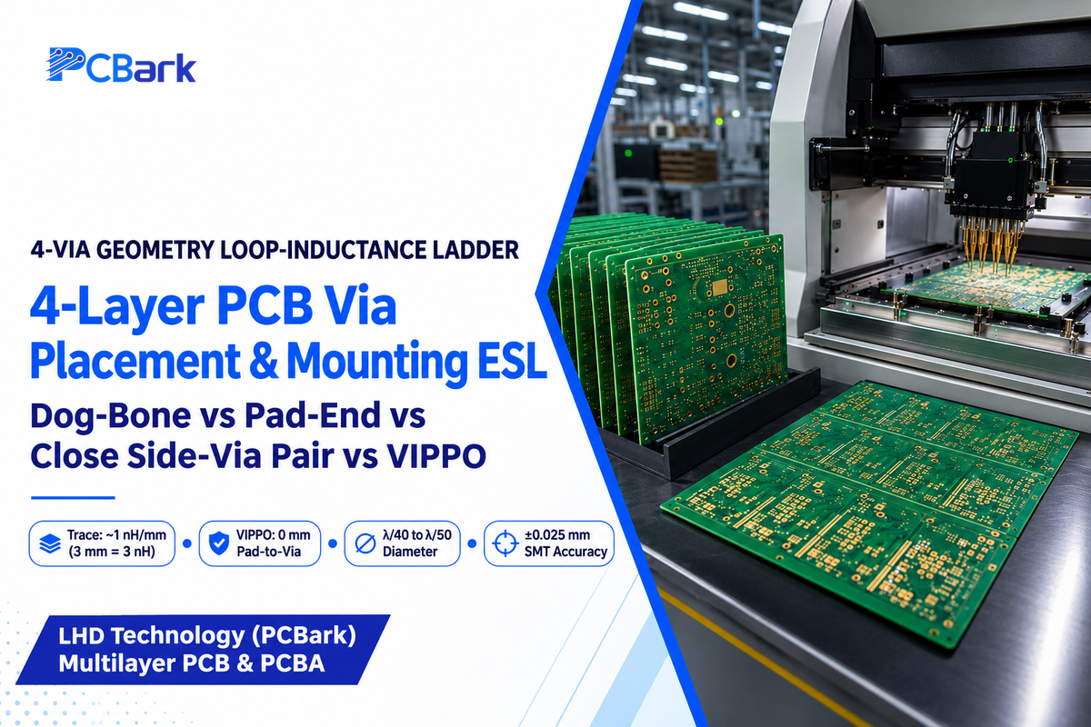
Even the lowest-inductance 0201 or 0306 capacitor fails if long PCB traces and large via loops choke its current path. Proper decoupling requires placing the capacitor beside the IC pin and dropping vias directly into closely spaced power and ground planes.
The EEVblog discussion refers to roughly 1 nH/mm for trace inductance; the inductance for the decoupling loop also assumes trace geometry and spacing as well as via placement. Based on that 1 nH/mm estimate, 3 mm of narrow trace adds 3 nH, more than six times the 450 pH bare-body ESL of a 0603 capacitor. A simple textbook formula for single-via barrel inductance Lvia ≈ 0.2 h [ln(4h/d) + 1] underpredicts real PCB mounting inductance. In the real world, the total loop inductance is governed by the mutual inductance of the power-and-ground via pair and the spreading inductance of the plane cavity.
As KYOCERA AVX (EPCI) specifies, the optimal pad configuration places the via directly within the capacitor pad (via-in-pad) to eliminate pad-to-via trace length. When via-in-pad is not allowed by the manufacturing rules, placing power and ground vias close together along the capacitor’s long side allows opposing vertical currents to cancel magnetic flux. We summarize these geometries in The 4-Via Geometry Loop-Inductance Ladder below. On multilayer boards, shallow connections from capacitor pads to the relevant power and ground planes shorten active via current paths. Closely spaced plane pairs in 4-layer PCB stackup fabrication with controlled L1-to-L2 prepreg thickness or 8-to-12-layer PCB stackups with adjacent power-ground plane pairs reduce plane spreading inductance. Increasing the number of layers alone does not shorten through-hole via barrels.
| Via Fanout Geometry (Worst to Best) | Trace & Via Routing Configuration | Loop Inductance Mechanism | Recommended Application Tier |
|---|---|---|---|
| Rung 1: Long Dog-Bone Trace Fanout | Vias placed several millimeters away at the ends of narrow traces | Extended narrow traces enlarge the vertical-and-horizontal magnetic loop area between the capacitor and return plane | Avoid on high-speed digital or RF supply pins |
| Rung 2: Standard Pad-End Vias | Single via placed immediately outside each short end of the SMD pad | Eliminates long traces, but full capacitor body length separates the via pair | General-purpose microcontrollers and Tier 2 mid-band rails |
| Rung 3: Close Side-Via Pair (Long-Side Vias) | Power and ground vias placed close together along the long side of the capacitor | Opposing vertical currents in closely spaced vias increase mutual flux cancellation (per EPCI) | High-speed clock buffers, FPGAs, and DDR memory rails |
| Rung 4: Via-in-Pad Plated Over (VIPPO) | Resin-filled and copper-capped vias placed directly inside the capacitor lands | 0 mm pad-to-via trace per EPCI; with ground on Layer 2, total loop inductance still includes power and ground via spacing, connected-plane depths, and return paths | 0.8 mm BGA backside arrays, SerDes, and GHz RF stages |
How Close Should a Decoupling Capacitor Be Placed to IC Power and Ground Pins?
Place high-frequency decoupling capacitors as close to the IC power supply pin as pad clearances allow, keeping the effective decoupling diameter within λ/40 to λ/50 of the wavelength of the highest-frequency noise. As KYOCERA AVX (EPCI) states, exceeding a λ/40 to λ/50 effective decoupling diameter around the pin introduces phase delay and loop inductance that diminish fast pulse suppression. In fine-pitch 0.8 mm BGA packages, the shortest vertical current paths are provided by using resin-filled VIPPO vias to mount 0201 or 0306 capacitors on the back of the PCB.
Decoupling in Circuit Design: Microcontrollers, Analog Op-Amps, Switching Regulators, and BGA Power Pins
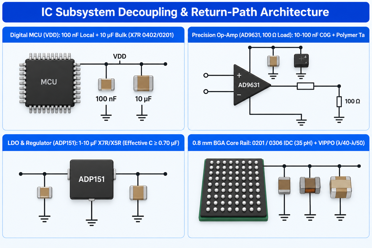
Different integrated circuit families require customized decoupling networks because digital CMOS gates create sharp current spikes, while analog op-amps and ADCs have ground-return distortion. A design that permits a digital microcontroller to run can still inject harmonic spurs into a precision operational amplifier if return currents share a trace near the amplifier input.
In All About Circuits’ test on an AD9631 op-amp driving a 100 Ω load, high-frequency supply return currents flowing through the decoupling capacitor coupled magnetically into the sensitive input pin. This coupling degraded second-harmonic distortion until the capacitor’s ground return was routed away from the input stage, often paired with ferrite bead PI-filter isolation on sensitive analog rails. Similarly, Missouri S&T’s 2025 IEEE EMCSIPI paper demonstrates that multi-pin BGA packages must be modeled as a multi-port impedance matrix (Z-matrix). In fine-pitch BGA PCB assembly, adding a decoupling capacitor at one port alters transfer impedances across neighboring BGA power pins.
| Subsystem / Circuit Type | Recommended Local & Bulk Network | Preferred Dielectric & Package | Critical Layout & Return-Path Rule |
|---|---|---|---|
| Digital IC / Microcontroller (VCC / VDD Pins) | 100 nF local per VDD pin + 10 μF bulk per rail as an initial configuration for conventional designs; high-frequency, multi-rail ICs require a network matched to their rail impedance targets | X7R 0402 / 0201 (derated for DC bias) | Keep pad-to-via connections short; even 10 MHz 74AC logic has >1 GHz edge harmonics, and package and mounting inductance govern capacitor impedance well above self-resonance |
| Precision Op-Amp (e.g., AD9631 Driving 100 Ω Load) & PLL/VCO | 10–100 nF local + 1–10 μF bulk bypass | Class I C0G/NP0 (zero microphonics) + polymer tantalum | Route capacitor ground return away from input pins to prevent second-harmonic distortion (All About Circuits) |
| LDO & Switching Regulator Output (e.g., ADP151) | 1 μF to 10 μF output bypass network | X7R/X5R MLCC (verified for CEFF ≥ 0.70 μF minimum) | Place bypass capacitor adjacent to regulator output and ground return pins to maintain loop stability across load steps |
| Fine-Pitch FPGA / Processor BGA Core Rail | Parallel array of 0201 MLCCs, 0306 IDCs (35 pH), or 4×4 LICA | 0201 X7R, 0306 LICC/IDC, or C4 flip-chip LICA | Mount on the BGA backside with resin-filled VIPPO vias, keeping the effective decoupling diameter within λ/40 to λ/50 |
2025–2026 High-Speed PDN Trends: Reverse-Geometry (LICC) and 3-Terminal MLCCs, Embedded Capacitance, and AEC-Q200
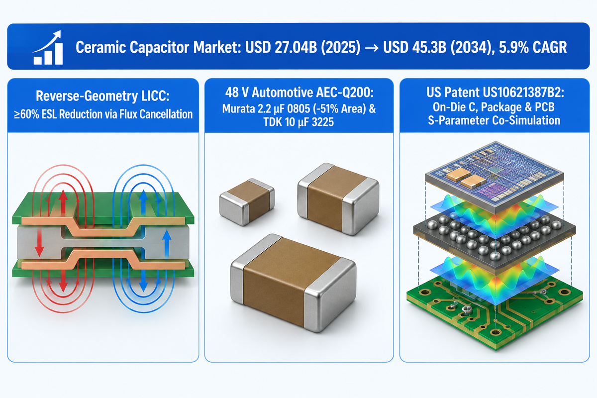
Rising AI accelerator currents and 48 V automotive power supplies are driving adoption of reverse-geometry MLCCs, 3-terminal feedthrough capacitors, AEC-Q200 soft terminations, and S-parameter co-design. According to Maximize Market Research’s industry report, the global ceramic capacitor market reached USD 27.04 Billion in 2025. It’s projected to grow at a 5.9% CAGR from 2026 to 2034 to reach USD 45.3 Billion by 2034.
Three hardware innovations lead this expansion. First, for high-speed digital decoupling, KYOCERA AVX (EPCI) highlights reverse-geometry Low Inductance Chip Capacitors (LICC, reducing ESL by 60% or more). In these, the input and output inductances cancel each other out. Second, in 48 V automotive and ADAS systems, Maximize Market Research cites Murata’s GCJ21BD72A225KE02 (2.2 μF, 100 Vdc, 0805 soft-termination MLCC cutting area by 51%). They also note Taiyo Yuden’s 220 μF 3225 AEC-Q200 MLCC and TDK’s CGA series 10 μF, 100 V 3225 X7R MLCC, which halves part count in 48 V rails. Third, at the frequencies where BGA package inductance limits the contribution of board-level MLCCs, package and on-die decoupling become more relevant. USPTO Patent US10621387B2 describes iterative time-domain and S-parameter co-simulation of on-die capacitance (CDIE), package inductance, and PCB planes to shift package-die resonance out of the active operating band.
SMD Decoupling Capacitor Pricing, Top Manufacturers, and Turnkey PCBA DFM Checklist
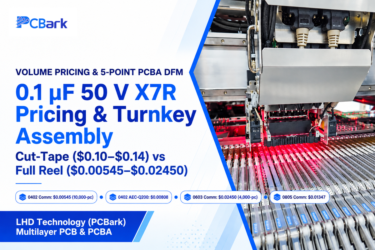
For the four listed distributor parts, full tape-and-reel purchasing reduces unit cost from $0.10–$0.14 on cut tape to $0.00545–$0.02450, while balanced pads reduce assembly defects. Leading global MLCC manufacturers include Murata, Samsung Electro-Mechanics, TDK, KYOCERA AVX, KEMET (Yageo), and Taiyo Yuden.
Published distributor data from DigiKey’s ceramic capacitor catalog illustrates the volume price gap across commercial and automotive 0.1 μF, 50 V, X7R, ±10% decoupling capacitors:
| Manufacturer & Part Number (MPN) | Package & Grade | Electrical Spec | Cut-Tape Unit Price (1 pc) | Full Tape-and-Reel Unit Price |
|---|---|---|---|---|
| Murata GRM155R71H104KE14D | 0402 Commercial | 0.1 μF, 50 V, X7R, ±10% | $0.10 / unit | $0.00545 / unit (10,000-pc reel) |
| Murata GCM155R71H104KE02D | 0402 Automotive AEC-Q200 | 0.1 μF, 50 V, X7R, ±10% | $0.10 / unit | $0.00808 / unit (10,000-pc reel) |
| KEMET C0603C104K5RACTU | 0603 Commercial | 0.1 μF, 50 V, X7R, ±10% | $0.14 / unit | $0.02450 / unit (4,000-pc reel) |
| Samsung CL21B104KBCNNNC | 0805 Commercial | 0.1 μF, 50 V, X7R, ±10% | $0.10 / unit | $0.01347 / unit (4,000-pc reel) |
Before releasing Gerbers and BOM files, LHD Technology (PCBark) performs a pre-production DFM review for 0201/0402 pad symmetry and thermal relief. Our team also manages turnkey PCB assembly BOM sourcing and AVL dielectric control. Use the 5-point checklist below to reduce open circuit tombstoning and flex-crack risks during SMT assembly.
The 5-Point MLCC DFM & Turnkey Assembly Verification Checklist
| DFM / BOM Checkpoint | Engineering Specification to Verify | Defect Mitigated on Production PCBA |
|---|---|---|
| 1. BOM Dielectric & Voltage Lock | Lock the exact MPN, dielectric code (C0G or X7R), and rated voltage (e.g., 50 V 0402 GRM155R71H104KE14D) | Prevents unauthorized substitutions; operating capacitance follows the selected part’s DC-bias curve, with temperature and tolerance also accounted for (the cited 100 μF / 6.3 V X5R example loses 50–70% at 3.3 V DC bias, leaving 30–50 μF; X7R capacitors can also suffer substantial DC-bias loss) |
| 2. Symmetric 0201 / 0402 Land Patterns | Use symmetric pad geometry based on IPC-7351, balanced thermal connections, and controlled solder paste deposition and placement | Reduces unequal wetting forces and tombstoning risk during reflow |
| 3. Resin-Filled VIPPO for Via-in-Pad | Specify epoxy resin plugging and copper capping over any via placed inside a capacitor pad | Prevents solder wicking down open via barrels and starved solder fillets on BGA backside arrays |
| 4. Board-Edge Flex-Crack Keep-Out | Keep 0805+ MLCCs away from depanelization lines and use soft-termination parts such as Murata’s GCJ series in high-stress locations | Reduces the risk of ceramic flex cracks and resulting power-to-ground shorts |
| 5. Polymer Tantalum Moisture Control | Moisture-sensitive parts kept within their specified storage and exposure limits do not require baking solely because they are moisture-sensitive | Moisture control reduces moisture-related reflow damage |
Frequently Asked Questions About Decoupling Capacitors
1. Are decoupling capacitors polarized on a PCB?
Local high-frequency decoupling capacitors at IC power pins are almost always non-polarized multilayer ceramic capacitorss (MLCCs) in 0201, 0402, or 0603 packages. They can be mounted in either orientation during automated pick-and-place assembly. Bulk decoupling capacitors such as aluminum electrolytics or solid tantalum capacitors rated from 10 μF to 1,000 μF are strictly polarized. Installing a polarized capacitor backwards causes a short circuit or thermal venting under power.
2. Can a decoupling capacitor value be too large for high-frequency noise?
Replacing 100 nF with 10 μF may worsen high-frequency decoupling if the replacement increases mounted inductance. With similar mounted inductance, the two capacitors can have similar impedance well above their self-resonant frequencies. Higher capacitance values lower the self-resonant frequency for a given inductance. Above the self-resonant frequency of a capacitor, its impedance is considered inductive, but it can still shunt switching harmonics if its mounted impedance is sufficiently low compared to the other current paths.
3. Do operational amplifiers and analog ADCs need decoupling capacitors on both supply rails?
Single-supply op-amps and ADCs use local supply-to-ground decoupling; dual-supply circuits also use negative-rail decoupling and may include capacitors between supply rails. An op-amp’s internal power supply rejection drops at high frequencies, allowing un-decoupled rail ripple to feed into the output. As shown on the AD9631 driving a 100 Ω load, route the capacitor’s ground return away from the input pins to prevent second-harmonic distortion.
4. What happens if you omit a decoupling capacitor on a digital microcontroller?
Transient switching currents flowing through trace inductance cause sharp supply voltage droop and ground bounce. This rail instability causes brown-out resets, corrupt memory writes, and clock jitter, and generates electromagnetic interference.
5. Why do PCB designers place a 0.1 μF and a 0.01 μF capacitor in parallel, and when does it backfire?
Designers extend frequency coverage by pairing a larger capacitor with a smaller one, but this backfires with low-ESR ceramics due to anti-resonance and an impedance spike. Between their two self-resonant frequencies, the inductive larger capacitor resonates in parallel with the capacitive smaller capacitor. For NextPCB’s example of a 10 μF capacitor (~5 MHz SRF) in parallel with a 100 nF capacitor (~50 MHz SRF), the reported 15-20 MHz peak doesn’t follow from bare component parameters alone. Mounting inductance and effective capacitance shift the peak frequency, while losses limit its height.
6. How does ambient temperature affect ceramic decoupling capacitor capacitance?
C0G/NP0 (Class I) ceramics show virtually zero temperature drift. In contrast, Class II dielectrics like X5R/X7R show ±15% drift across their operating temperature range and lose additional capacitance with DC bias.
7. When should you use an electrolytic or tantalum capacitor alongside ceramic decoupling capacitors?
Tier 1 bulk electrolytic or polymer tantalum capacitors in the cited 10–1,000 μF range supply additional transient charge when the regulator and local ceramic network can’t keep rail droop within the allowed limit. Required effective capacitance follows the transient charge deficit and allowed droop, while ESR adds a voltage step proportional to the transient current.
References & Sources
- Analog Devices — Low Dropout Regulators and Why the Choice of Bypass Capacitor Matters. Covers CEFF = 0.719 μF at 1.8 V bias, ADP151 droop (80 mV to 70 mV), MLCC microphonics, and the 3-reflow polymer tantalum limit.
- EDN Network (AVX) — Choosing Decoupling Capacitors. Mentions the 0.1 μF rule limits, 450 pH ESL on 0603 MLCCs, >75% LICC ESL reduction, 35 pH 0306 IDCs, and 4×4 LICA arrays.
- The European Passive Components Institute (KYOCERA AVX) — Low Inductance Ceramic Capacitors for High-Speed Decoupling. Talks about the 100 nF 0603 RLC response, parallel scaling (n·C, ESL/n, ESR/n), λ/40-λ/50 diameter, via-in-pad, and >60% LICC ESL reduction.
- NextPCB — Bulk vs. Decoupling Capacitor PCB Strategy. Documents the three-tier decoupling hierarchy, 15–20 MHz parallel anti-resonance peak, and 50–70% DC bias loss on 100 μF 6.3 V X5R at 3.3 V.
- International Electrotechnical Commission (IEC) — IEC 60384-21:2024 Edition 4.0. Defines fixed surface-mount Class 1 ceramic capacitors, including C0G and U2J temperature coefficients and board deflection tests.
- Missouri University of Science and Technology — Efficient Decoupling Capacitor Impact Calculation (2025 IEEE EMCSIPI). Studies the impact of insertion loss in multi-port PDN impedance matrices for decoupling capacitor placement.
- All About Circuits — How to Use Decoupling Capacitor Placement to Reduce Harmonic Distortion. Analyzes supply return current coupling on an AD9631 op-amp driving a 100 Ω load.
- EEVblog Electronics Community Forum — Decoupling Capacitor Trace Length for Low-Frequency Applications. Mentions ~1 nH/mm trace inductance and >1 GHz edge harmonics on 10 MHz 74AC logic.
- United States Patent and Trademark Office (USPTO) — US Patent US10621387B2. Addresses dynamic PDN droop, L·dI/dt, switching charge CDIE and S-parameter co-simulation.
- Maximize Market Research — Global Ceramic Capacitor Market Report (2025–2034). Reports the USD 27.04B to USD 45.3B (5.9% CAGR) forecast and Murata, Taiyo Yuden, and TDK automotive MLCCs.
- DigiKey Electronics — Ceramic Capacitors Parametric Catalog & Pricing. Includes pricing (full-reel and cut-tape) for Murata, KEMET, and Samsung 0.1 μF 50 V X7R MLCCs.
Editorial & Technical Review: Authored by GW and reviewed by the LHD Technology (PCBark) PCB & PCBA engineering team.
WHY WE WRITE THIS
About PCBark Engineering Insights
PCBark shares technical PCB fabrication and assembly guides based on real engineering review and manufacturing experience. We help teams compare materials, stackups, DFM risks, component sourcing, inspection plans, and production routes before they move from prototype to volume builds.
16+ yrs EMS experience
1-42 PCB layers
500,000 m2 annual PCB capacity
IPC Class 2/3 build discipline
DFM + test review