Get in touch with PCBark Company



Quick turn PCB assembly is the compressed fabrication, sourcing, and assembly process that delivers a fully fabricated, populated, and tested printed circuit board in as little as 24 hours instead of 2+ weeks. Whether that promise comes true for your particular board is less a function of which vendor you choose, and more a function of four things fully within your control before you ever upload a file: your board’s design complexity, your file package, your acceptance-class choice, and how you weigh the rush cost against the schedule you’re trying to save. This guide walks through the buyer’s half of that equation, the half every quick-turn PCB assembly capability page omits.
Quick Specs
| Fastest realistic tier | 24 hours, 2-6 layer FR-4, ≤10 boards, files DFM-clean |
| Core file package | Gerber (RS-274X), BOM with MPNs, pick-and-place/centroid, assembly drawing, NC drill |
| Typical acceptance class | IPC-A-610 Class 2 for prototypes; Class 3 only when the end application requires it |
| Top delay cause | Incomplete or ambiguous BOM — not fabrication speed |
| Current acceptance standard | IPC-A-610 Revision J (3/2024) + IPC J-STD-001 Revision J (4/2024) |
What “Quick-Turn” Actually Means as a Build Category
A quick-turn PCB assembly squeezes board fabrication, component sourcing, SMT placement, and testing into one rapid cycle that can run anywhere from 24 hours for a basic two-layer PCB prototype to several days for an eight-to-ten-layer board carrying BGAs. PCBark’s own quick-turn line publishes a four-band schedule from 24 hours to 10 days by layer count and quantity — a starting reference before the factors below explain why.
An engineer chasing a Friday investor demo and a hobbyist ordering a weekend quick turn prototype pcb are both shopping the same lead-time bands, but only one of them can afford to guess wrong about which tier their board actually qualifies for — a rough sense of quick turn pcb assembly cost before you submit files saves a renegotiated date later. The term shows up written several ways across the pcb industry — quick-turn, quick turn, quickturn, and quickturn pcb are all the same thing — and rapid turnaround board manufacturing now shows up on most pcb assembly services pages, from US quickturn pcbs shops to offshore quickturn pcbs suppliers, as a standard production services offering rather than a rush-only exception.
The one factor which many companies’ capability pages don’t offer a consideration of isn’t a matter of your file quality; rather, it’s production line availability. Buyers on r/PrintedCircuitBoard report that dedicated quick-turn production lines are “generally booked weeks or months in advance” for genuine rush work, and that a real rush order for a single 4-layer panel commonly runs $1,000 or more with assembly starting around $2,500 — nowhere near a normal quotation, more like an entirely different cost category. “Quick-turn” simply tells you how fast production of your board runs, once you’re on a line, and doesn’t in any way indicate whether there are any free production lines at the exact time that you would require.
The Clock-Start File Checklist, What Actually Starts (and Stalls) a Rush Build
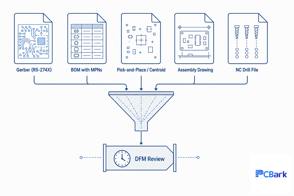
From a technical perspective, the “production clock” of an order doesn’t even start until your file is reviewed by the shop’s engineering team to make sure that your files will be suitable for production (this is what they call the “design-for-manufacturing,” or “DFM” review), and it’s certainly not triggered when you click the ‘Submit’ button. There are five components of a “ready-to-build” file package: A Gerber file for each individual layer in RS-274X format; A complete Bill of Materials with manufacturer part numbers; a pick-and-place or “centroid” file; an assembly drawing indicating where special components should be placed; and an NC drill file for hole sizes and coordinates. Any file missing will put a halt on your DFM process before the actual construction can even commence. PCB designers submitting the drill file should also call out plated and non-plated holes separately rather than lumping them together — a common source of NC drill mismatches that shops catch in review anyway, but catching it yourself is faster than waiting for the question back.
| File | Common rejection cause | How to prevent it |
|---|---|---|
| Gerber (RS-274X) | Missing layer or undefined solder-mask opening | Export full layer stack; visually check in a Gerber viewer before submitting |
| BOM | Missing manufacturer part numbers or unresolved substitutes | Include MPN + reference designator + approved alternate for every line |
| BOM | Unmarked Do-Not-Install positions | Explicitly flag DNI lines, don’t leave them blank |
| Pick-and-place / centroid | Wrong origin or rotation convention | Use a consistent origin; double-check BGA and fine-pitch rotation |
| Pick-and-place / centroid | Coordinate mismatch vs. Gerber silkscreen | Cross-check reference designator positions against the board outline |
| Assembly drawing | No polarity marking for diodes/electrolytics/IC pin 1 | Mark polarity explicitly; avoid silkscreen overlapping pads |
| NC drill | Hole-size table doesn’t match Gerber pad sizes | Regenerate drill file from the same CAD revision as final Gerbers |
| All files | Files from different design revisions submitted together | Export the full package in one session, right before submission |
| All files | No fiducials for automated placement | Add board-level fiducials for SMT pick-and-place reference |
What files do I need for a quick-turn PCB quote?
A same-day quick-turn quote needs five complete files: Gerber data (RS-274X format), a complete Bill of Materials with manufacturer part numbers and reference designators, a component pick-and-place file, an assembly drawing showing polarity and special instructions, and an NC drill file with hole coordinates and sizes.
An emerging XML-based alternative to Gerber is IPC-2581, which consolidates BOM, netlist, layer, and stack-up information into a single file. Whichever format you use, compile and send all five files as one unit — a single file arriving after the others is one of the most avoidable causes of DFM delay, and it erodes your rush window before fabrication ever starts.
💡 Pro Tip
Pre-submission component checking – be it against your DigiKey or Mouser list, or your assembler’s parts checker – identifies long-lead or obsolete parts when they are still easily swappable with approved alternatives. The cost of checking only after submission can be a one-week lead time instead of a 48-hour quote.
The 4-Lever Speed Penalty, Why Your Design Missed the 24-Hour Window
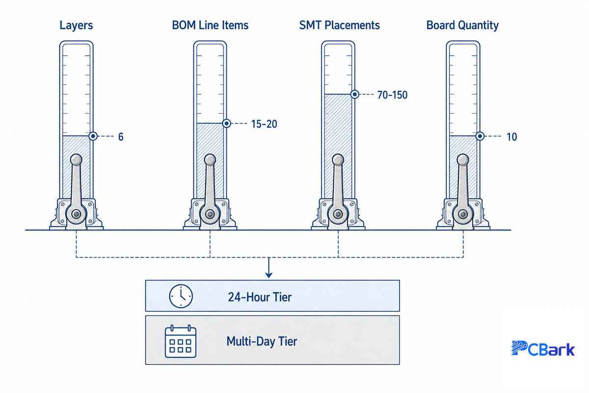
Four gates must be cleared for a board to reach the fastest turnaround tier.
And it’s your pcb design – not your fabrication shop – who sets each gate: the number of layers on the PCB, number of line items on the BOM, number of placements per board on the SMT process, and the area of the PCB panel. PCBark’s Quick-Turn Feasibility Gate displays the thresholds to enter each tier – ≤10 boards, a BOM of ≤15-20 line items, ≤70-150 SMT placements per board, and ≤6 layers for the 24-hour tier. What that page doesn’t do is explain how those values are determined or the consequence of exceeding them for your schedule.
Each added layer means another lamination cycle, which pushes fabrication out of the same-day tier and into the multi-day tier once a board passes roughly six layers, across every provider that publishes lead times by layer count. Both line-item count and placement count drive assembly time directly; for instance, a board with 400 SMT placements would take about three times as much line time as one with 150 placements (without accounting for any lead times due to component availability). Panel area influences all three aspects – with greater area, even the same level of complexity per area unit requires proportionally more cycles on the solder-paste printer and the reflow oven.
📐 Engineering Note
An Example: If your design were 8 layers, with 200 BOM line items and approximately 400 SMT placements on each side, it likely falls within the 5-day range, rather than the 24-hour range. Simply for its number of layers (which is greater than the threshold around six layers), it can’t enter the fastest band, and the number of placements more than doubles the time it would take to populate a 150-placement board, which the fastest bands are generally based around. A minimum trace/space of 4 mil (0.10mm) is achievable on the 0.10 mm laser microvias of quick-turn HDI lines, but every additional lamination cycle to accommodate blind/buried vias necessitates another fabrication step not typically covered by fast-turn bands.
Minimum Trace Width, Solder Mask, and the Small Print That Slows a Rush Order
Sub-4-mil trace/space, solder-mask-defined pads, and blind/buried vias are all achievable on a quick turn pcb fabrication line, but each one requires a process step beyond what the fastest speeds are scoped for. That’s why boards using them end up in the 3-7 day range rather than the 24-48 hour range. That difference isn’t dictated by acceptance class; Class 2 and Class 3 of IPC-A-610 simply dictate inspection density and defect tolerance, not the physical build speed. Speeding a build only compresses queue and coordination time — AOI, X-ray on BGAs, and functional test all run the same regardless of turn speed. IPC-A-610 Revision J (March 2024) and the companion IPC J-STD-001 Revision J (April 2024) — both released together in the same revision cycle — establish today’s standards, so check them for detailed acceptance criteria, or see PCBark’s IPC-A-610 Class 2 vs Class 3 Selector to quickly clarify for your design.
The Design-Choice Cost Multiplier, What Actually Drives Your Quote

What’s your lead time? – The other half of the quick-turn equation is the “How fast do you really need it?” side, which we covered at a macro level in PCBark’s China-vs-US Quick-Turn Cost and Speed Crosswalk. Now, let’s get into the design details that influence lead times on a board you may have already assigned to build location.
| Your choice | Typical quote impact |
|---|---|
| Component selection (BOM) | Largest single lever — component/BOM cost is typically the majority of total assembled-board cost, commonly cited in the 40-60% range by PCB assemblers, though the exact split varies by BOM and is worth confirming on your specific quote |
| Each added layer | Material and lamination-cycle cost stacks per layer, on top of the layer’s speed penalty |
| Acceptance class (2 vs 3) | Class 3 adds inspection density, not fabrication time — cost impact is in test labor, not the build |
| Turn-speed tier | Same-day/24-hour tiers carry the steepest premium over standard lead time of any lever in this table |
| Turnkey vs. partial turnkey | Full turnkey trades a sourcing margin for speed and single-point accountability; partial suits teams already holding critical inventory |
For a real world validation of how price scales with speed, look no further than this thread from the r/PrintedcircuitBoard subreddit. Buyers confirm the “excellent work” provided by fast US houses comes “with up to few days turnaround if you’re willing to pay”, but add “very pricey overall.” The consensus isn’t from the vendors, it’s from customers who use them – price is relative to speed in practice.
The Rush-or-Wait Test, Is Expediting Even Worth It for This Board?
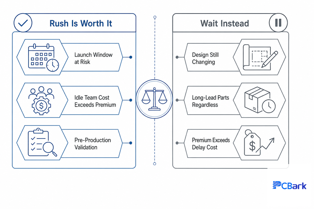
All quick-turn capability pages assume you’re already planning on going fast. Before handing over the rush premium, three self-diagnosis questions are worth running through — design-for-manufacturing research has long argued that cost and schedule decisions made this early in a product’s development cycle carry the most weight on the final outcome, so the rush-or-wait call belongs before you submit files, not after.
Ask yourself:
✔ Rush is worth it when
- A slipped date push a launch into the next selling window
- An idle engineering or test team costs more per day than the rush premium
- You’re validating a design before a much larger production commitment
⚠ Standard lead time makes more sense when
- The board still need a design change before production anyway
- Your BOM has genuinely long-lead components no rush tier can source faster
- The 100-300% rush premium exceeds the cost of the delay itself
How to Get Quick-Turn PCB Assembly Actually Started
Getting a quick-turn order going in less than 24 hours requires submitting those five standard files – gerber, BOM with MPNs, pick-and-place, assembly drawing, and NC drill – all together to allow for single-pass DFM review. Then, the next step is to quickly identify where your board falls among the four design factors that define speeds (layer count, number of BOM items, number of placements, and panel area), so you can then ask for the 24-hour pricing, instead of learning you don’t qualify after placing the order. Once your board is design-complete, and assuming you’ve all your components in-house or on an approved list, a quick-turn line is often able to begin production the same day files are approved, but if you exceed one of those four levers, requesting the 3-5 Day estimate up front saves disappointment and renegotiation mid-production.
The Missed-Window Chain, Where Quick-Turn Orders Actually Fail
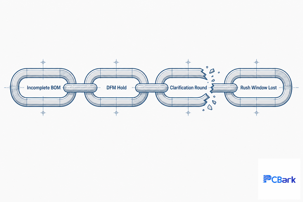
Quick-turn failure often gets blamed on the shop, as in, file completeness alone. Trade-press coverage of the quick-turn-to-production transition and independent buyer experience both point to a wider chain of events, and one of the clearest examples has nothing to do with the board shop at all.
“The mistake people make is thinking a 24-hour board skips inspection. It doesn’t. What we cut is the dead time between fab, parts, and the line, not the SPI step or the AOI pass. Rushing the assembly process never changes the quality of the pcb that ships — a rushed board that fails at your bench costs everyone more than a board that ships a day later, so the DFM gate is non-negotiable even on expedited orders.”
PCBark Engineering Team, Process & Quality
As one engineer described a prototype that “arrived with a subtle mistake making them unusable” – a subtle mistake of two sensors sharing the same I2C slave address because the address-select pin was left floating rather than tied to VCC. That couldn’t have been prevented by speeding up fabrication. That was a design review mistake that a 24-hour turn only served to accelerate. The key pattern to learn here: speed compresses manufacturing time, not the commitment to design accuracy.
| Failure Type | Typical cause | Typical delay added |
|---|---|---|
| Incomplete BOM | Missing MPN or unresolved substitute part | 1-3 days of clarification before fabrication starts |
| Design-level error | Address conflicts, floating pins, footprint mismatches | Full re-spin — the fastest build clock can’t fix a bad design |
| Capacity/queue mismatch | Rush line already booked out | Days to weeks, independent of file quality |
| Long-lead component | Single hard-to-source part in an otherwise complete BOM | Can stall the whole order regardless of turn tier requested |
| Acceptance-class mismatch | Class 3 application ordered as Class 2 (or vice versa) | Rework or re-inspection after the fact |
| Mixed-revision files | Gerber, BOM, and pick-and-place exported from different design revisions | DFM review flags the mismatch, adding a clarification round |
| Missing fiducials | No board-level reference points for automated placement | Placement-accuracy rework on fine-pitch/BGA boards |
| Untested feasibility | Board submitted at a rush tier without checking layer/BOM/placement thresholds first | Quote comes back at a slower tier than requested, losing a negotiation cycle |
| Consigned-parts delay | Buyer-supplied components arrive late or fail incoming inspection | Shifts the critical path from the shop’s queue to the buyer’s shipping |
The 6-Point Quick-Turn Readiness Audit, Vetting a Partner Before You Commit
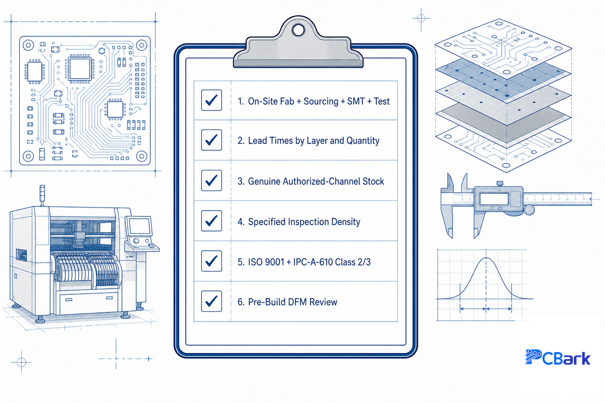
The existence of multiple Reddit threads on “USA quick turn pcb recommendations” indicates a reasonable suspicion about vendor claims: almost every quick turn pcb manufacturer’s capability page advertises “24 hour turn times,” yet buyers keep asking peers to name a shop that actually delivered on that promise. A team that skips this audit and simply picks the fastest quoted number tends to find out the hard way, mid-build, that “24 hours” had unstated conditions attached. Six quick questions can weed out a capable partner from a potential disappointment, based on readily available vendor information.
- On-site fab, sourcing, SMT and test (no out sourcing between separate vendors)
- Detailed lead times by layer count and quantity (no single generic ‘1-5 days’ number)
- Genuine stock in authorized channels (no late ordering after your job starts)
- Specified inspection density (AOI on each board, BGAs via X-ray, no ‘quality checks’)
- Relevant certifications (at least ISO 9001, plus explicit mention of IPC-A-610 Class 2/3)
- Pre-build DFM review (no shipping back of failed boards to start the clock again)
PCBark’s in-house fabrication capability spans up to 42-layer boards, with 8 SMT lines producing roughly 9 million placements per day. PCBark is ISO 9001:2015, IPC-A-610 Class 2/3, and J-STD-001 certified. The type of detail PCBark provided here are precisely the ones to probe before trusting any quick-turn provider. Whether you call the vendor a pcb production shop or one of many pcb services in a given region, the same six checks apply across prototyping and low-volume production alike — a quickturn prototype run and the low-volume order that follows it should go through the identical vetting.
Industry Outlook, What’s Changing in Quick-Turn Assembly for 2026

Search activity across the entire quick-turn/DFM/IPC-class search group is showing an obvious spike August-September 2025 with a reversion back to a more level, lower trend line through mid-2026, but the rise/fall pattern itself is clear and shared among what otherwise are fairly unrelated search terms. The most plausible driver is semiconductor and component lead-time normalization — a shift in the same underlying manufacturing-process economics that ongoing NIST engineering research tracks at the design-and-manufacturing level: after a couple of years of allocation-and-shortage dynamics that made “rush” the default posture for any time-sensitive board, 2026 industry reporting describes a market that’s “selectively constrained” rather than broadly shortage-driven, with some MCU vendors back to 12-20 week lead times rather than the 30-40+ week extremes of the shortage era. As sourcing friction eases, some of the urgency that used to justify paying a rush premium eases with it.
That doesn’t mean quick-turn demand is going away — it means the driver is shifting from “my supply chain forced this” toward “my development schedule needs this,” a design-stage decision rather than a supply-chain emergency. A team that used to pay a same-day premium every time a distributor quoted a 30-week lead time now has more room to plan a standard rapid pcb prototyping run instead, and reserve the same 100-300% rush markup typically cited earlier in this guide’s cost breakdown for the OEM projects that genuinely carry schedule risk. That shift matters in practice because it changes which boards are worth expediting: the same 4-lever feasibility check covered earlier in this guide, not a blanket “always rush” instinct left over from the shortage years, is what should decide it — the certifications and in-house process control a shop like PCBark runs don’t change with the calendar, but the case for paying the premium does. At least two 2026 industry outlooks independently note rising component density and a move toward mixed-technology builds becoming standard rather than exceptional in the pcb manufacturing process, which complicates DFM review even as urgency-driven rush orders cool. The practical takeaway: the file-readiness and design-choice habits covered above become more valuable, not less, as boards get denser.
Frequently Asked Questions
Q: What is the minimum trace width allowed on a quick-turn board?
View Answer
quick-turn lines typically support down to 4 mil (0.10 mm) traces and spaces, and will produce 0.10 mm laser microvias on an HDI build. It is layer-count dependent, with heavier copper (1 oz+) generally needing a bit more trace width to manage the tolerances required of etching, and thinner copper on typical 2-6 layer FR-4 boards will produce tighter geometries within the bounds of a particular line’s specification. If your design will push to less than 4 mils, be sure to verify capabilities at a specific shop, as sub-4mil designs are sometimes pushed into a slower turn-tier irrespective of the number of layers. Minimum feature size and silk screen feature size both tighten together as trace/space drops, which is exactly why sub-4-mil designs slip into a slower band regardless of layer count.
Q: What’s the shipping schedule difference between a 2-layer and a 6-8 layer quick-turn board?
View Answer
The fastest turn (usually 24 hr) is the simple, 2-layer FR-4 board on a quick-turn line; file ready and passed through DFM. Any build requiring lamination will jump to a 48 hr – or longer – category, primarily due to the laminations which represent additional PCB builds nested within the existing PCB. The fact that an order is marked “rush” does not inherently change the length of any given lamination process step.
Q: Can I supply my own critical components on a quick-turn order (partial turnkey)?
View Answer
Yes — partial turnkey lets you ship critical or long-lead items you may already possess while the assembler procures the remaining components, useful when you already have a good price or an approved source for specific components. On a quick-turn timeline, however, you also sacrifice some speed since your consigned items need to be received and checked before they are placed into the fabrication process; that adds your component lead time and inbound inspection time to your critical path. If you just want speed on quick-turn timeline, then you need full turnkey (shop sourcing from stocking or authorized sources).
Q: What’s the single most common reason a “24-hour” quote turns into 5 days?
View Answer
An inaccurate or incomplete BOM line item – missing MPN, undecided substitution, DNI item not marked, rather than complexity of the board, since it causes a DFM hold before fabrication can start.
Q: Should a production board (not just a prototype) ever go through a quick-turn line?
View Answer
Yes, on low-to-mid volume runs (say, 5-500 boards) where the engineering and the files can be carried over from the prototype build with no vendor requalification-as this uses the same review process as your prototype design went through during DFM.
Q: How do I actually get quick-turn PCB assembly started?
View Answer
Submit your five essential files together (Gerber, BOM with MPNs, pick-and-place, NC drill, assembly drawing), confirm your board sits inside the four speed-lever thresholds for your target tier, and request a landed-cost-and-schedule estimate rather than a bare unit price.
Why We Write This
Buyer-side file-prep and design choices decide whether a rush order actually hits its window, and this quick-turn PCB assembly guide walks through exactly that — the questions our own engineers hear most often after an expediting request has already been placed. It’s meant to sit alongside, not repeat, our quick-turn capability page, which covers what we build; this covers what gets your board there fastest. Reviewed by the Shenzhen Linghangda Technology Co., Ltd. technical team.
Related Articles
References & Sources
- Acceptability of Electronic Assemblies (IPC A-610J-2024) — ANSI
- IPC Releases “J” Revisions to Two Leading Standards for Electronics Assembly — IPC
- New Directions in Design for Manufacturing — University of Maryland Institute for Systems Research
- Assessment of Selected Research Programs and Goals, Engineering Laboratory, FY2024 — NIST
- Electrical Insulation of Conformally Coated Printed Circuit Assemblies — IEEE Xplore (cites IPC-A-610 as the industry-approved acceptability standard)
- Fresh PCB Concepts: Quick-turn Prototype PCB Fabrication to Production Volume — I-Connect007

![Drone PCB Design Guide: IPC Class & Manufacturing [2026]](https://pcbark.com/wp-content/uploads/2026/07/drone-pcb-design-guide-featured-150x150.png)