Get in touch with PCBark Company



A 32-42 layer PCB is an ultra-high-layer multilayer board built for applications where 16-24 layers cannot route the required signal density — HPC/AI server backplanes, 400G-800G telecom line cards, and aerospace/defense systems. Working at this tier demands sequential lamination, blind/buried via strategy, and tightly controlled impedance, and it is not automatically better than a lower layer count for a design that does not need it.
Key Takeaways
- Out of the design guides that are currently ranking for this subject, the most influential one (pcbsync.com, NeuronWriter score 73) lists no credible clickable sources; every number mentioned in this guide can be traced back to an official IPC standard, patent, or academic source that’s provided in the References section.
- Yield on acceptable layers drops sharply after approximately 30, a fact independently verified by two unrelated manufacturers rather than just a single vendor’s product page.
- While through-hole-only via strategies aren’t inherently inadequate for speeds of 25 Gbps and higher, it’s the independently verified via performance of the fabricator, rather than the specified via type, that ultimately predicts a design’s success.
- Stacked-microvia reliability isn’t consistent; for instance, two-level stacked microvias have been shown to endure approximately 20 times more thermal cycles compared to four-level stacked microvias.
- If your project design doesn’t necessitate the 32-42 layer tier, a well-designed 16-24 layer stack-up with well-planned planes will be more cost-effective and easier to schedule than an overly designed 32-42 layer board.
Quick Specs: 32-42 Layer PCB Design Envelope
- Layer count: 32 or above
- Min trace/space: 0.050mm (2 mil)
- Controlled impedance: ±5%
- Layer-to-layer registration: ±35µm
- Plated hole copper: ≥35µm
- Sequential lamination cycles: 4-6
- Bow & twist: ≤0.30%
- Typical materials: Rogers, Isola, Panasonic Megtron, hybrid stacks
Sample values from a commercial 32-42 layer process capability sheet (documented tier level, not an overall industry limit).
This guide is intended for design engineers, not for purchasing agents. If your goal is to find a fabricator and understand how to confirm their equipment, certifications, and pricing, that’s a different task than pcb stackup design; this guide focuses on the stack-up planning, via design, and signal integrity decisions that are made before any Gerber file leaves your desk for production.
What Is a 32-42 Layer PCB, and Where Is It Actually Used?

A PCB with 32-42 individual copper layers bonded together with dielectric material between each pair is known as a 32-42 layer PCB. It represents the highest tier in multilayer PCBs, far beyond the 4-16 layers used in consumer electronics and the 16-24 layers commonly found in networking line cards and industrial controls.
The actual applications fall into four main categories: High-Performance Computing (HPC) and Artificial Intelligence (AI) accelerator backplane server boards, which require extremely high routing density for multiple HBM memory interfaces and chip-to-chip links; 400G/800G telecom switch and router line cards supporting multiple 112 Gbps PAM4 SerDes channels; Aerospace and defense systems — the kind covered in NASA’s own High-Speed PCB Design Guide — including radar signal processing boards and avionics computers; and advanced medical imaging equipment, such as CT and MRI data-acquisition subsystems. The common characteristic among these four applications isn’t a general need for more layers, but rather a specific combination of factors: BGA packages with very high pin counts (typically 1,500+ pins), multiple high-speed differential interfaces, each needing its own reference plane, and a power delivery system with a greater number of independent voltage rails than can be accommodated cleanly within a lower-layer stack-up.
This layer-stacking discipline applies whether the end application is an HPC/AI backplane, telecommunications infrastructure, or aerospace systems — what changes between them is qualification burden, not the underlying physics of registration, copper foils, and dielectric layers bonding together under heat and pressure. Before committing to a full 32-42 layer design, most engineering teams request pcb prototypes at a lower layer count first, both to validate the schematic and to confirm a candidate fabricator’s stated pcb capabilities on power distribution and process control actually match what the datasheet claims — precision manufacturing claims are easy to state and harder to verify without a physical board in hand.
💡 Key Takeaway
The number of layers is an indication of a design need and not a design intent in and of itself. Every board design that’s included in the following list has some inherent need or driver-whether that need be to achieve a certain pin count, interface count, or to support a specific power-rail count-and in the next section, we break that driver down into a handy checklist to check your board before signing up for the premium.
Do You Actually Need 32-42 Layers? The 3-Question Layer-Count Necessity Threshold
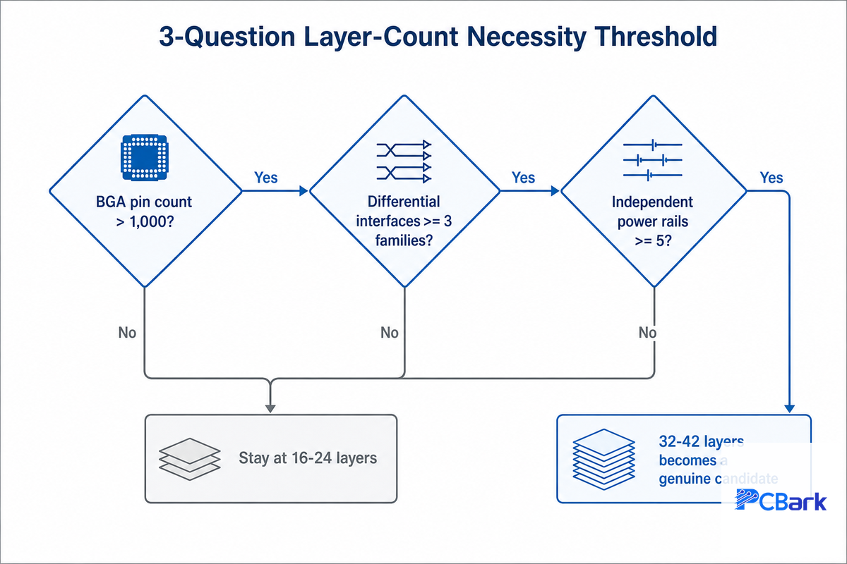
The 3-Question Layer-Count Necessity Threshold is a filter: is your BGA pin count alone, or differential-interface count alone, or your independent power-rail count alone greater than what a 16-24 layer stackup will support with a clean reference plane to each signal layer?
If all three questions can be answered “no”, then a right-sized lower-layer board will beat an over-specified 32-42 layer board on cost, schedule, and — perhaps counter-intuitively — reliability, as each new lamination process is a risk for registration skew.
| Design Driver | Threshold | Recommendation |
|---|---|---|
| BGA pin count | <1,000 pins | 16-24 layers is usually sufficient |
| BGA pin count | ≥1,500 pins | 32-42 layers becomes a genuine candidate |
| High-speed differential interfaces | 1-2 interface families | Dedicated reference planes fit within 16-24 layers |
| High-speed differential interfaces | 3+ concurrent families (PCIe 5.0, DDR5, 400G+) | Each family competing for reference planes pushes past 24 layers |
| Independent power rails | 2-4 rails | Shared plane pairs usually work |
| Independent power rails | 5+ rails, high current | Dedicated plane pairs per rail forces additional layers |
Two independent fabricators validate this fundamental danger without being asked about it by each other. One comments, “After layer counts exceed 30, the yield may decrease dramatically, making total cost go up,” the raw words from a businessman making boards for a living rather than some vendors’ advertising pitch. A separate registration accuracy study from Missouri University of Science and Technology mentions, “Poor layer-to-layer registration in high-layer builds…can cause inner layer shorts, annular ring reduction, via breakout, impedance deviation and yield loss”-the exact same series of failure, explained in a different way, a few dozen microns off of target is sufficient.
None of this means don’t pick the tier when you absolutely need it — it just means make sure you ask the three questions before you go all in. I’ve got a real world data point from an actual working engineer on what this looks like in practice: a designer said their board was 2 layers to start, and ended up being 14 over the lifetime of a product that spanned a few years, and over that time they also tracked its speed going from 6MHz to 133MHz and trace widths down from 12 mil to 4 mil — they tracked the required layers up over time instead of picking too high up from day one. The cost curves similarly follow that same exponential path: publicly available fabrication data would indicate that a 32 layer pcb can cost between 12x and 18x that of a baseline 2 layer board (rough order of magnitude, not a real quote, you need to get a quote specific to your stackup), and this increase then increases, rather than steadily continues once you exceed roughly 30 layers due to the cost of low loss materials, number of laminations, etc.
⚠️ Common Misconception
“More layers is always safer” is just about the exact reverse of how real engineers approach design. In fact, one well-regarded signal integrity consulting expert, among others, has made a general case for the idea that keeping layer count and design complexity to a minimum (as is often supported by best practices) usually out performs blindly throwing layers and planes at the problem – finding the minimum required layer count.
Building the Stackup: Plane-Pair Assignment and Symmetry
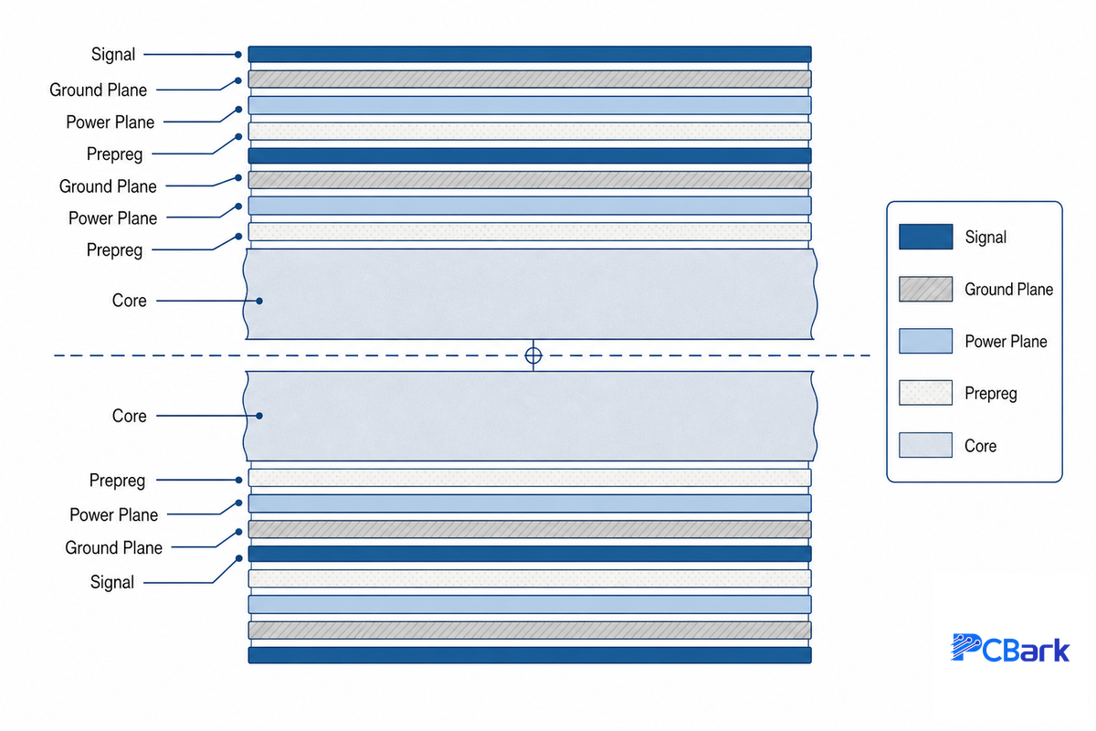
Once that necessity threshold verifies this layer, stackup planning commences with plane-pair assignment, not total layer count — the same plane-adjacency principle laid out in NASA’s High-Speed PCB Design Guide. You’ve got to have a reference plane adjacent to every signal layer-a signal layer referencing a plane more than two layers removed wouldn’t support good signal integrity and likely fail any EMC tests, regardless of the pcb’s overall layer count. What usually transpires in planning: first, designate power and ground plane pairs anchored about the highest speed signal layers, then spread signal layers between these pairs such that every signal layer lies at most one layer away from the reference layer; finally, insert the lowest-speed signals and any secondary power into the remaining layers.
The Registration Margin Gauge is what should define your tolerances: an officially issued fabricator process capability document lists a layer-to-layer registration as tight as ±35µm; compare this value, then, when asking a fabricator for “tight tolerance.” A specific, documented ±35µm is meaningfully tighter than the 5-mil (0.127mm) “rule of thumb” most would apply for 50-layer and higher PCBs, although that latter figure is itself an industry rule of thumb, not an independently standardized benchmark — treat the ±35µm figure as the number to verify per fabricator, not the comparison ratio. Each lamination cycle you add sequentially depletes some portion of the tolerance; this makes balanced copper distribution an important factor, alongside layer count. Because uneven copper distribution causes differential expansion and resulting warpage when hot pressuring, it can produce a physically deformed PCB, which only shows up after it’s assembled.
Stackup Planning Checklist
- Each signal layer require its neighbor reference layer; don’t plan it away.
- Place the entire trace length for any signal pair on a single layer.
- Centrally located traces of power/ground plans are balanced by those that extend outwardly toward each outer edge.
- You map your via locations prior to initiating signal routing.
When you get the stackup wrong at this early point, in the words of an EDA provider’s guide to design engineers, it’s “one of the most common errors leading to fabrication failures and rejects”-and it’s far cheaper to revise in software than after a board is first run.
HDI Vias: The Via Strategy Spectrum
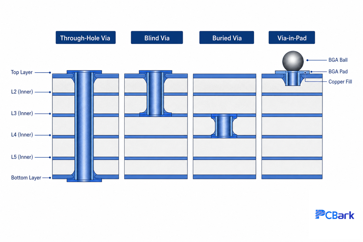
Blind, buried and via-in-pad structures exist for the sole purpose of overcoming one challenge; on boards with no more than through-holes, we “burn” routing resources unnecessarily on unused layers as we snake the through-hole vias across the stack; by forum, among the engineers currently involved in board design, the universal agreement is that the need for blind and buried vias arise only when it’s necessitated by component density and available space-and not as a standard approach. On the Via Strategy Spectrum, from bottom up, the cheapest approach is the via through, which causes the most routing loss; blind via, on the other hand, will interconnect the outer most to the inner most layers of the stack; the buried via connects interior layers only, and via-in-pad with copper fill can facilitate routing for tightly-spaced BGA pads — the pad-reduction approach behind US9711441B2, a granted patent for a reduced PTH pad enabling core routing, is one documented example of engineering around that exact tradeoff.
What Are Blind and Buried Vias in a PCB?
Blind vias reach an outside layer and one or more inner layers without penetrating the whole board; buried vias contact two or more inner layers without contacting any outside layer. Both help regain wiring paths otherwise unavailable across all the layers they traverse-the kind of issue a through-hole via on a high pin-count BGA where escape routing is limiting creates.
Before specifying any type of via, the first step is to do the aspect ratio math. Aspect ratio is the drill depth divided by the finished diameter of the hole. Using typical “32-42 Layer Capability” documented minimums (a 0.10mm mechanical hole and a 0.050mm laser via) an example stack-up 3mm in thickness and using a 0.10mm mechanical drill yields an aspect ratio of 3.0mm/0.10mm = 30:1. This already strains the limits of reliably plating mechanical holes. Using a 0.050mm laser micro-via, a similar 3mm section couldn’t support the same drill depth without an extremely limited aspect ratio because the micro-via doesn’t penetrate the entire stack-that’s precisely the rationale for building with a stack of blind and buried construction instead of a single long through-hole. Calculate this number against your stack thickness and minimum hole size before settling on your strategy.
| Via Type | Connects | Best For |
|---|---|---|
| Through-hole | Top to bottom, all layers | Low-speed nets, power/ground stitching |
| Blind via | Outer layer to inner layer(s) | BGA escape from outer layers |
| Buried via | Inner layer(s) only | Freeing inner routing channels |
| Via-in-pad (copper-filled) | Directly under a BGA pad | Fine-pitch BGA escape density |
Not all vias are equally reliable, a nuance often missed in purely routing discussions. Literature based on testing stacked microvias revealed the 2-level stack to be roughly 20 times more reliable in thermal cycles to failure than the 4-level stack, based on the samples used. This doesn’t negate the need for a higher stack in some designs-but it does make “the number of levels of stacked microvias” a distinct reliability variable and not one inherent to just “blind vs. buried vs. via-in-pad,” which should prompt asking the fabricator for stacked-via test data.
Another aspect beyond routing: A 2023 study evaluating the use of 112 Gbps PAM4 signaled confirmed that even through-hole PTHs are viable at that speed, provided the fabricator’s via geometry and plating are independently validated. That same study, however, when duplicating the design on another fabricator’s lines, observed a reduction in via bandwidth. This isn’t a takeaway of “PTHs are good and why are you even reading this-just stick with them.” It’s that your chosen via type on the datasheet is only half the equation-fabricator performance has to be proven out, not presumed.
Signal Integrity and Impedance Control at 25+ Gbps
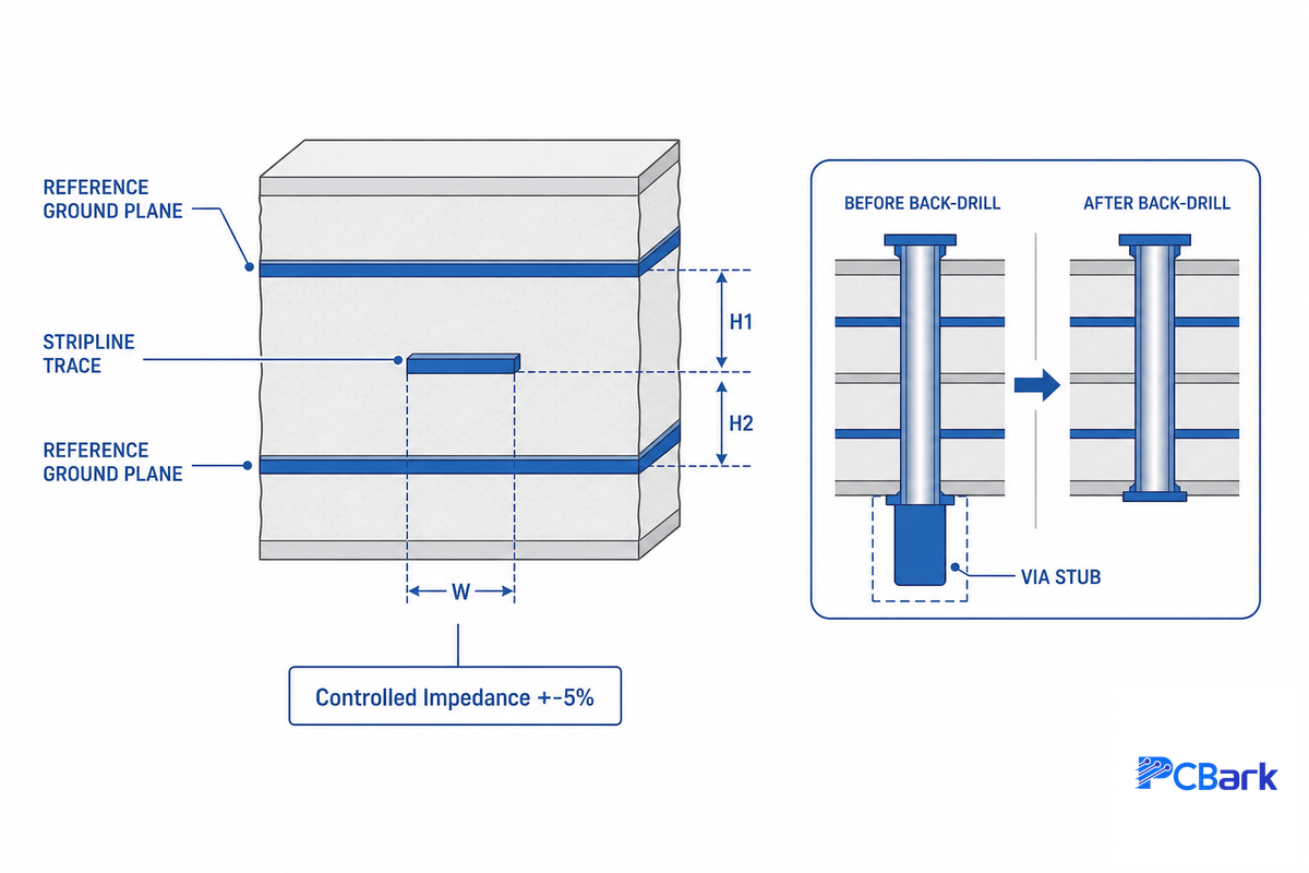
Controlled Impedance Because any signal transmitted on a trace is a transmission line rather than a simple wire, a discontinuity anywhere along the transmission line (e.g. a via, a layer transition, a connector) will cause part of the signal to reflect back toward the source. With low frequencies, those reflections settle out before causing trouble. But at speeds above 25 Gbps or so, the bit interval is so short that the reflected signal will arrive at the receiver when the next bit is still being sampled, and the eye diagram will close. This is the underlying WHY of two design rules that are always present in any 32-42 layer stack-up: controlled impedance tolerance, and back-drilling.
A documented process capability sheet for a 32-42 layer process will specify 5% controlled impedance tolerance on the Maximum tier (a tighter spec than the 10% generally encountered at 4-12 layers), because a tight differential pair must have identical impedance on both conductors of the pair to avoid mode conversion – a mechanism whereby energy escapes the differential mode and becomes a common-mode signal that radiates EMI. Back-drilling removes the unneeded portion of a through-hole via after it connects the required inner layers. At frequencies greater than 25 Gbps, an unused portion of the via above its connect point becomes a stub antenna resonating at a frequency of interest. Therefore, above approximately 25 Gbps, back-drilling isn’t an optional item. Material complex permittivity must be precisely measured over the signal spectrum to properly account for it during the simulation – even the NIST Technical Note on Dielectric Measurement notes this measurement is required for accurate analysis. “ Accurate complex-permittivity measurement … can significantly impact analysis of printed circuit board traces for their suitability for transmitting signals with negligible signal distortion and crosstalk.”
What Is the 3-W Rule in PCB Design?
The 3-W rule states that to maintain acceptable EMI on a dense multilayer stack-up, the trace-to-trace spacing (S) should be at least three times the trace width (W), measured edge to edge. Too tight spacing increases coupling between adjacent traces; too loose wastes limited board space.
Because board space on a 32-42 layer stack-up is usually under tremendous pressure from high-density BGAs (ball-grid arrays), the 3-W rule is frequently challenged in the interest of routing density, which means the practice of differential-pair-aware layer assignment (keeping high-speed differential pairs segregated on a few dedicated layers) becomes even more critical.
What Is the 20-H Rule for Power Plane Shielding?
The 20-H rule addresses another EMI path: electromagnetic field fringing out of a power and ground plane. Recessing the power plane from the ground plane by a distance equal to 20 times the dielectric spacing between the two planes (H) limits that fringing field.
At a 32-42 layer board, with potentially six to eight ground planes and many different power voltages, this rule can impose a significant constraint on board size and plane shape, rather than simply being a small footnote in the design documentation.
| Tier | Impedance Tolerance | Typical Registration |
|---|---|---|
| Standard (4-12L) | ±10% | ±75µm |
| Best (14-24L) | ±8% | ±50µm |
| Maximum (32L+) | ±5% | ±35µm |
“The way good engineers get to a reliable design is to reduce complexity-adding planes and layers doesn’t magically get safer if there’s no underlying stackup discipline.”
Materials Selection: Low-Loss Laminates for Ultra-High-Layer Stacks

Rigid pcbs at this tier live and die on prepreg selection just as much as core-laminate selection — the resin system bonding each pair of copper traces to its neighboring layer has to survive four to six lamination cycles without degrading, which is a materially different requirement than a quick-turn 4-layer prototype ever faces.
Material selection at this tier is a Dk/Df-versus-cost tradeoff-there isn’t a single ‘best’ choice. Standard FR-4 and high-Tg FR-4 can still be the solution for power planes and low-speed signal layers for the 32-42 layers; only those layers that carry 25+ Gbps signal needs low loss material- Rogers, Isola, Panasonic Megtron-family-and it specifically is low Df at high frequencies that matters.
A hybrid stack is commonly employed that only use low-loss material for the high-speed signal layers, using FR-4 on the rest of the layers on a 32-42 layer build to manage cost.
Material selection is also the other factor of impedance, discussed in the previous section: dielectrics, like their thicknesses, factor into an impedance calculation, not the other way around.
When sending an impedance target with stack-up and material specification, make sure they’re solved in tandem, not separately. Ongoing material R&D reflects the same direction, with a patent application filed in 2024 for an inorganic thin non-woven dielectric claiming its suitability in “high layer count applications, as well as in HDI printed circuit board,” confirming that low-loss dielectric material development is keeping pace with the other trends at this tier.
| Material | Best For | Typical Core Thickness | Relative Cost |
|---|---|---|---|
| Standard FR-4 | Rarely used alone at this tier | 100-200µm | Baseline (1x) |
| High-Tg FR-4 | Power planes, low-speed signals | 100-200µm | ~1.2x |
| Halogen-free FR-4 | Compliance-driven power/ground layers | 100-200µm | ~1.3x |
| Mid-loss laminate (Megtron-4 class) | 10-25 Gbps signals | 75-150µm | ~2.5x |
| Low-loss laminate (Megtron-6 class) | 25-56 Gbps signals | 50-125µm | ~4x |
| Rogers (ceramic-filled low-loss) | 25-56 Gbps signals, RF-adjacent nets | 50-125µm | ~4-5x |
| Ultra low-loss laminate (Megtron-7 class) | 56+ Gbps signals | 50-100µm | ~6x |
| Hybrid stack (mixed low-loss + FR-4) | Cost-managed high-speed designs | Varies by layer | ~2-3x blended |
Relative cost factors and thickness ranges are directional, compiled from industry-published stackup guidance — confirm exact figures with your material supplier and fabricator, as pricing and availability vary by supplier agreement and volume.
What Sequential Lamination Means for Your Design Choices
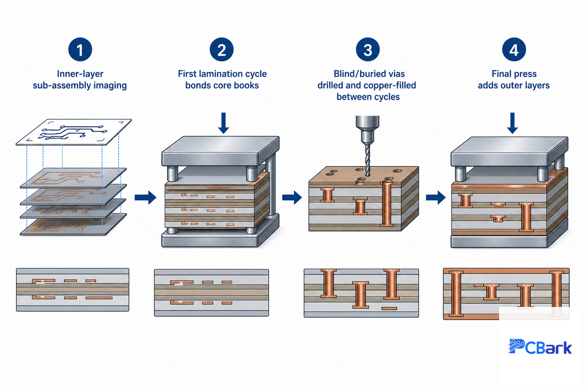
A 32-42 layer build isn’t a one-shot press; it’s constructed as multiple sub-assemblies of inner layers, each bonded to a substrate core and then pressed over 4 to 6 lamination cycles, during which inter-layer vias are drilled, plated and copper-filled.
The impact on the design is that each press cycle subjects all previous layers to a final application of pressure and temperature, and thus presents another opportunity for loss in registration as mentioned previously.
Engineering Note: Patented literature describing plating processes for through-holes discusses the fact that on sequential press constructions, air/solvents can be trapped in plated through-holes, a defect mechanism that isn’t seen on single-process builds, which is why inspecting between laminations, not just the final step, is normal on high layer counts.
During sequential lamination, inner layers have to be placed sequentially within pre-pregged core layers and subsequently pressed under heat and pressure. This lamination occurs with cycles that repeat up to dozens of times for some boards, and a failed inspection during an early lamination cycle must be addressed immediately because there’s a subsequent lamination cycle, and it’s usually too late to reach the defective layer. Excessive resin flow can leave a starve area within the dielectric or, conversely, can cause the dielectric to be completely removed (e.g. creating voids in the trace). Similarly, too little flow will create gaps. On top of that, uneven pressure across the panel will be embedded within the laminated layers. None of this is a reason to avoid sequential lamination when a board design truly requires that many layers, but it’s the reason the concept of “layer count is a free variable” shouldn’t influence the mindset of the design engineer. Each layer the design adds represents a laminating cycle that consumes additional resources, time, and budget, rather than simply a passive increment in signal routing capability.
Common Design Mistakes: The High-Layer Failure-Mode Anatomy
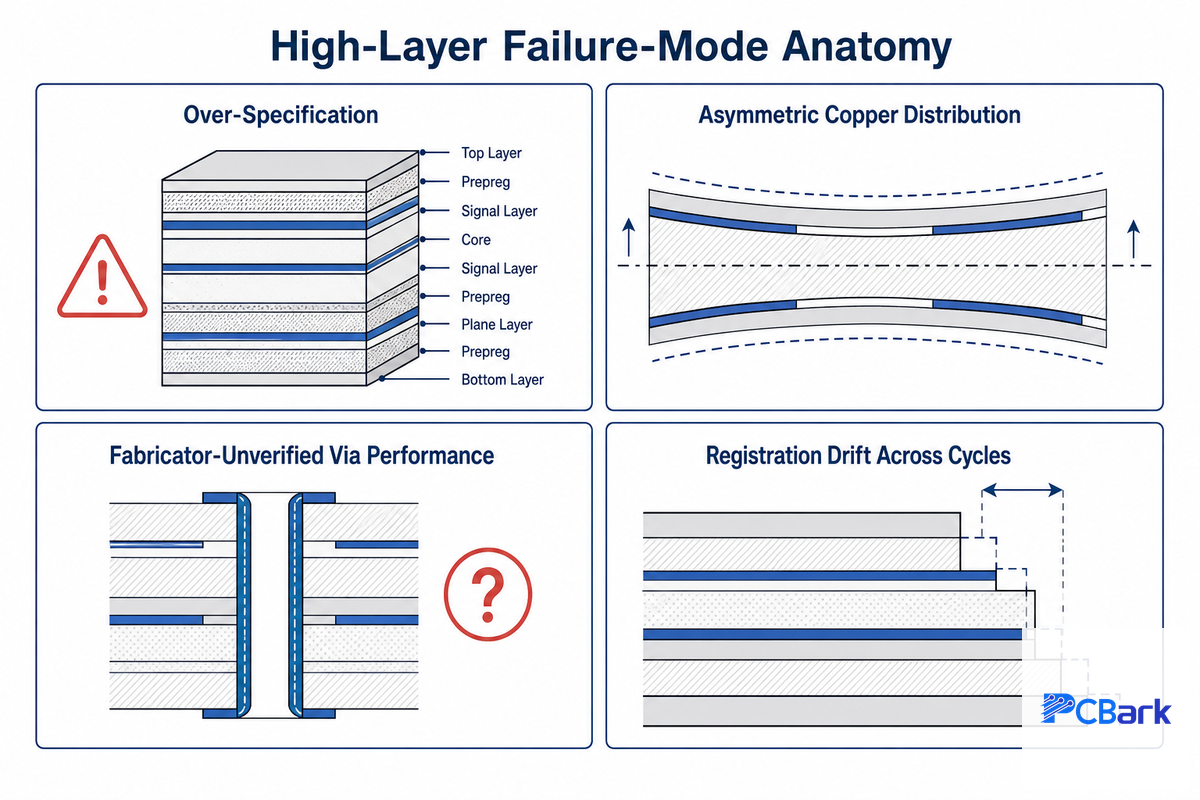
Four broad categories form the Anatomy of High-Layer Failure — common reasons for the failure of 32-42 layer designs the first time they’re manufactured — each of which stems from a different fundamental cause and each of which has a specific remedy.
1. Over-specification. Adding 32-42 layers where a 16-24 layer design would have sufficed based on Layer Count Necessity Threshold criteria, as described in earlier parts of this guide. In the previous section, the guide referenced how a 2-layer board became a 14-layer design over years of increasing demand — that’s a healthy upward progression in layer count; defaulting to the maximum tier in a design from the outset of the first iteration is an unhealthy and costly one, especially in cases where it’s difficult to justify adding layers to gain unneeded performance.
2. Asymmetric copper distribution. If there’s an uneven amount of copper on the inner and outer layers, the resulting differential expansion of materials during lamination can lead to bowed or twisted panels — something that wouldn’t have occurred with an evenly distributed copper stackup (covered in the Stackup section).
3. Fabricator-unverified via performance. Assuming that a given set of vias that work on one fabricator’s production line will have equivalent performance at another fabricator’s plant is an extremely costly assumption to make. As mentioned previously, as 112 Gbps PAM4 research reveals, even the identical design run at a different fabricator’s can experience a noticeable drop in via bandwidth — a finding consistent with the Missouri University of Science and Technology crosstalk analysis cited earlier — which is another reason that relying on a standard data sheet to define the characteristics of specific types of vias can’t replace actual fabricator-specific testing.
4. Registration drift across lamination cycles. Treat the registration tolerance not as one rigid figure but rather as a budget that diminishes as additional layers are sequentially added during the laminating process, thus increasing the likelihood that a 6-layer board will fail to meet a specification it technically meets at 4-layer.
Design File Readiness: What Your Documentation Needs Before Submission

Evaluating your fabricator’s equipment and certifications is distinct from ensuring your own design files are ready for delivery to that fabricator – the majority of guides about high layer count PCBs primarily discuss the former. For a 32-42 layer PCB to have a realistic chance of success, the design files should contain enough inherent information to enable a fabricator’s process engineer to assess the feasibility without needing an iterative exchange of clarifying emails — the same completeness standard NASA’s High-Speed PCB Design Guide holds design files to.
Every pcb stack-up design brings its own manufacturing challenges once layer counts climb this high, and file types matter as much as content: a design file package that’s ambiguous about via transitions between layers, or that assumes the fabricator will infer how the copper layers are laminated together and plated with copper, invites the exact clarifying-email cycle this section exists to avoid. Advanced manufacturing techniques for a multilayer circuit at this tier — sequential lamination, controlled-depth drilling, per-core inspection — only pay off when the design file itself is unambiguous about what it’s asking the fabricator to build. Teams running multiple pcb projects at this layer count learn to standardize their pcb manufacturing process notes once, rather than re-deriving it design by design; the alternative is relearning the same manufacturing challenges on every new multilayer pcb fabrication run.
A clear stack-up diagram that shows how the pcb layers connect — including exactly where the electrical connections between layers occur — gives a fabricator’s process-control team a real understanding of pcb behavior under lamination heat, rather than a set of complex designs they have to reverse-engineer; that’s the difference between a smooth multilayer pcb manufacturing process and a scrapped lot mid-way through pcb manufacturing and assembly. That same handoff also determines whether component assembly runs smoothly afterward: once fabrication finishes, a 32-42 layer board destined for SMT placement and reflow still has to clear pcb assembly and automated optical inspection (AOI) before it’s ready to ship, and a fabricator with in-house multilayer pcb manufacturing and pcb assembly capability under one roof avoids handing a dense, internal-layer-heavy board between two separate vendors mid-build.
✔ Impedance targets stated per net class (not just a single board-wide value), with the dielectric stackup they were calculated against
✔ A via callout table listing every via type used (through-hole, blind, buried, via-in-pad) with target aspect ratio for each
✔ Layer-to-layer registration tolerance and symmetric copper-weight callouts on the stackup drawing, not just a layer count
✔ Back-drill depth specification for every net running above roughly 25 Gbps, with the stub-length target stated explicitly
✔ Surface finish and solder mask specification confirmed against the chosen dielectric material’s processing temperature
✔ A request for fabricator-specific via performance data (registration coupon, microsection report) on a representative prior lot — not just a capability claim
That request is the direct, practical answer to the fabricator-verification gap mentioned earlier in this article: design that calls out real coupon evidence up-front puts the burden of proof before fabrication ever starts, rather than after a bad board come back from assembly with a prototype that shouldn’t have been ordered at all.
Industry Outlook: What’s Driving Demand for Higher Layer Counts

The concrete driver of increased demand for 32-42 layer counts isn’t an industry-wide trend like “growth”, but instead it’s AI and HPC server architecture, which is now coming out in earnest — and the risk for a design team that treats this as a someday problem is a scramble at quote time, once low-loss material lead times turn out not to compress the way FR-4 lead times do. High HBM memory interfaces, dense chip-to-chip connectivity, and multi-hundred-watt (500W+) board power all represent the exact same three factors from the Layer-Count Necessity Threshold table earlier in this article, converging on a single board — the same combination that shows up not only in hyperscale data-center racks but increasingly in aerospace avionics backplanes and telecom line-card RFQs that PCBark’s own engineering team fields. Trade reporting notes AI’s share of overall PCB demand growing substantially between 2025 and 2026, and that matches the kind of requests we’re seeing for this class of design.
For 2026-2027 design cycles, the practical action plan is this: if your board designs are trending towards 400G/800G SerDes or multiple-HBM memory configurations, go ahead and plan for low-loss and/or hybrid dielectric availability from day one, not just at quote time. Teams that wait until the quote stage to raise materials tend to hit the same gap: the fabricator flags a 12+ week lead time on a low-loss laminate that FR-4 would have shipped in days, and the schedule slip lands on the design team, not the material supplier. Lead times on the low-loss materials used for 25Gbps+ don’t compress nearly as quickly as those for FR-4, and with patents on inorganic dielectric materials emerging, that class isn’t static.
Frequently Asked Questions
Q: What is the use of a 32-42 layer PCB?
View Answer
Use 32-42 layer counts when 16-24 layers simply aren’t enough to route all the needed signals: This class is seen in high-performance and AI servers using multiple HBM memory channels and high-speed chip-to-chip links, in 400G/800G-speed telecom line cards with many high-speed SerDes interfaces, in aerospace and defense avionics and radar systems, and in advanced medical imaging data acquisition boards. All are characterized by high-pin-count BGAs, high-speed, multiple-concurrent interfaces, and complex power-delivery challenges.
Q: How thick is a 32-42 layer PCB?
View Answer
Common board thickness for this layer count is 2.8mm – 6.0mm, dependent on the stackup itself, material selection, and copper weight. A 32-42 layer capability document we referenced earlier specified a max board size of 600x1200mm with a thickness range of 0.3 – 6.0mm; the precise figure will depend on your board stackup and the copper weights you are using.
Q: What software is best for designing a 32-42 layer PCB layout?
View Answer
Professional, high-layer-count design is generally conducted using Cadence Allegro, Siemens Xpedition, or Altium Designer- tools with the advanced signal integrity analysis, constraint management, and fabrication output capabilities required for a 32-42 layer stackup. While other tools can technically handle a design of this size, they typically lack the deep constraint control and signal-integrity features required for optimal performance without considerable manual intervention.
Q: How do multilayer PCBs handle heat dissipation at this layer count?
View Answer
For 32-42 layer counts, the main methods of heat dissipation involve not only board surface, but copper plane mass and via-based thermal paths-power and ground planes provide laterally-directed heat conduction from heat-generating areas, while thermal vias situated beneath heat-generating components can channel heat down the stack to the back plane, other planes, or to a backplane heatsink interface. Even the choice of material is indirectly involved: high-Tg boards withstand the higher heat experienced during rework or repeated reflow processes better than standard FR-4, which is important when assembling these dense, high-layer-count boards.
Q: Can any PCB manufacturer produce 32-42 layer boards?
View Answer
No — which means, from the designer’s perspective, your design file has to include the documentation needed for any unfamiliar manufacturer to be able to check manufacturability-such as an impedance call-out list per net class, a stack-up diagram and tolerances, and a via call-out table (see Design File Readiness).
Q: What is the highest layer count ever achieved in a PCB?
View Answer
Well beyond commercial levels-Research-level and test-fixture PCBs are being produced in higher layer counts; an AI wafer-test fixture with 124 layers was reported in 2025 (exceeding the long-standing 108-layer figure, which itself exceeded an earlier, reported-on theoretical research PCB from 2012). Those high numbers are for research/test equipment and are not representative of PCBs in commercial production equipment, however; these devices can justify much higher scrap rates than the typical PCB in an HPC system. For all real, commercially-produced ultra-high-layer PCBs used in the HPC/aerospace/telecom sector, that’s around the 32-42 layer count this document covers, and that’s the layer count most design engineers specify.
Request a DFM Review on Your High-Layer Stackup →
Why We Wrote This Guide
We build 32-42 layer boards ourselves, and we noticed that the highest-ranking design guide for this exact keyword cites no independently verifiable source for any of its numbers — every citation is a book title or a standard number without a link.
This guide takes the opposite approach: every specification claim traces to a real, checkable source, listed below, and every design recommendation is scoped to what the evidence actually support, including the places where the honest answer is “verify this with your specific fabricator” rather than a confident-sounding guess.
References & Sources
- IPC-6012D-AM1 AmendmentIPC (Association Connecting Electronics Industries)
- High-Speed PCB Design GuideNASA
- Analytical Prediction of Crosstalk among Vias in Multilayer Printed Circuit BoardsMissouri University of Science and Technology
- NIST Technical Note on Dielectric MeasurementNational Institute of Standards and Technology
- A Contribution to Printed Circuit Boards’ MiniaturizationASME Digital Collection
- WO2024211571A1: Inorganic Thin Non-Woven Dielectrics in Printed Circuit BoardsGoogle Patents (2024)
- US9711441B2: Reduced PTH Pad for Enabling Core RoutingGoogle Patents
- DE102004045451B4: Galvanic Process for Filling Through-HolesGoogle Patents
- What Is New in IPC-6012 Revision FSummit Interconnect
- Getting Your Layer Stack RightAltium
- Differential Pairs: From Basic Concepts to Advanced PCB RoutingCadence
- Via Stub Resonance and Signal IntegrityEMA Design Automation
![Drone PCB Design Guide: IPC Class & Manufacturing [2026]](https://pcbark.com/wp-content/uploads/2026/07/drone-pcb-design-guide-featured-150x150.png)