Get in touch with PCBark Company


![16-24 Layer PCB: Stackup, Lamination & Design Guide [2026]](https://pcbark.com/wp-content/uploads/2026/07/16-24-layer-pcb-guide-featured-2.png)
The 16-24 layer pcb resides where the routing density, power-plane count, and signal integrity demands exceed what a 4-12 layer board can deliver – i.e. where most server back planes, telecom switches, and avionics boards actually live. In this paper we discuss stackup architecture, why we should resort to sequential lamination, the approach to blind and buried via implementation, impedance verification, and a scheme for auditing the fabricator prior to releasing a design to manufacturing.
A 16-24 layer PCB is a multilayer printed circuit board built from 16 to 24 conductive copper layers, most commonly requiring multi-cycle sequential lamination once blind or buried vias are added. IPC-6012F (the current rigid-board qualification standard, released October 2023) governs its qualification testing, and it commonly serves server/HPC backplanes, networking switches, and aerospace/defense avionics, applications where routing density and multi-domain power delivery exceed what smaller multilayer boards can provide.
Key Points
- The cost of layers is non-linear. From IPC’s Relative Cost Index table a 24-layer board is 6.42 times the cost of an 8-layer. Not 3 times.
- Sequential lamination gets triggered once a design adds blind or buried vias (very common in this range of layers) — it’s the via structure that dictates this, not the number of layers per se.
- Not necessarily a good thing – 3 different fabrication firms agree – stackup discipline wins not layer count.
- AI accelerator boards already come with 16-24+ layers (28-40+ layers for new platforms); this layer band is the current production main-stream, not the ceiling.
- Initial reflow may be successful in a microvia but later reveal itself at high temperature and low pressure through solder overflow onto the land – even with full visual inspection.
Quick Specs
| Layer range | 16-24 conductive copper layers |
| Board thickness (24L reference) | ~160 mil stack height in a published 24-layer, 10-signal-layer academic reference design |
| Layer-to-layer registration | ±50 µm (~2 mil) typical for high-layer-count boards, independently reported by two fabricators |
| Impedance tolerance | ±10% standard capability, ±5-7% achievable at premium tier |
| Governing qualification standard | IPC-6012F (rel. 2023-10-18) |
| Relative cost vs 8-layer baseline | 16L: 3.42x · 20L: 4.80x · 24L: 6.42x |
What Actually Counts as a 16-24 Layer PCB
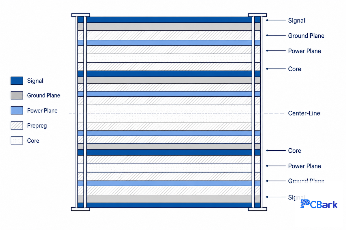
NASA’s board-workmanship standard offers the following definition that’s general enough to apply without strict boundaries: “a composite structure that uses point-to-point interconnections to form an electronic circuit… including constructions that are single-sided, double-sided, multi-layer, rigid, rigid-flex and flex” — a definition broad enough to cover nearly any multilayer board, 16-24 layers included.
The 16-to-24-layer range actually owes more to a structural threshold, however: you require separated ground and power planes instead of just another layer for the actual traces and components, the stackup needs to remain symmetric for laminating without deformation, and when you start adding blind or buried vias, the board won’t just be laid up once anymore.
The Missouri University of Science and Technology 2025 class project study took up a real 24-layer design: 10 signal layers within a 160-mil overall stack up, 1.3 mil stripline dielectric. This is a considerable step up from a 4-6 layer consumer board, and it’s why the design questions raised here, stackup symmetry, lamination ordering, via selection, impedance control, begin to matter at this range in a way they don’t much below it.
📐 Engineering Note
IPC-9151 (the PCQR² fabricator capability benchmark) standardizes test panels at certain layer counts, including precisely 24 layers, on 18″x24″ panels with through, 1/2/3-deep blind-via, and buried-core structures. If a fabricator can’t point to PCQR²-equivalent qualification data at your target layer count, that’s a real gap in capability.
Whether the spec sheet calls it a 16 layer PCB, a 20 layer PCB, or simply a high layer count PCB, the dividing line described above stays the same regardless of the exact number in between.
Stackup Design and Layer Arrangement for 16-24 Layers
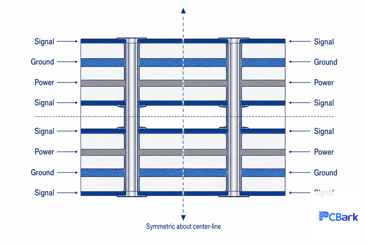
The ruling principle at this layer count is the same as at 10 layers, just iterated many more times: every signal layer must have an adjacent reference plane, each of the outer layers and inner layers has a dedicated role in the stackup, and the entire stack-up has to be symmetric from top to bottom relative to the center of the board in order to avoid warping during lamination. Rick Hartley, a signal integrity veteran at Applied Innovation, laid out the fundamental physics simply: “since signal layers should always be routed one dielectric layer away from a return plane, having more than six signal layers in a 10-layer stack-up isn’t a good idea.”
“Due to the very thin dielectrics in high-layer-count boards, those of the 10- and 12-layer variety have extremely low plane impedance and excellent signal quality, if properly stacked.”
Rick Hartley, Applied Innovation, EE Times
Scale that rule to 24 layers and the same signal-to-reference-plane discipline holds, which is exactly what the Missouri S&T case study demonstrated in practice: targeting 100 Ω differential impedance on a stripline differential pair signal layer, the design achieved 99.76 Ω (a 0.24 Ω error), -1.19 dB/inch insertion loss against a -1.2 dB/inch target, and -78.29 dB far-end crosstalk against a -60 dB target. That’s what a properly stacked high-layer board looks like when the reference-plane rule is followed consistently, figures from one published academic case study, not a cross-validated industry average, so treat them as a proof point rather than a guaranteed result on every design.
However, this doesn’t happen by itself. One case, for example, with a 24-layer, 3.0mm-thick board had top/bottom layer copper density imbalances serious enough to have failed flatness requirements without correction. Also flagged in that same review was a customer spec for 4mil maximum backdrill stubs that was considered too aggressive given the board’s thickness. It’s risky to maintain such tight stubs on such a thick board while ensuring adequate plating in the vias; 5-6 mil minimum was recommended instead.
Failure to properly balance copper density can result in non-visible failures. One CAM engineer described designing a stackup in which all the power planes were located on one side of the board, with the signal traces all on the opposite side. When finished, the board warped badly after reflow and looked like “a potato chip.” Compounding the problem, the first few units tested fine, and the board’s warpage became apparent in field use only after six months of operation when the warped board had pulled enough BGAs out of contact to cause failures.
| Layer Count | Relative Cost Index | Typical Routing Density | Complexity Tier |
|---|---|---|---|
| 8 (baseline) | 1.00x | reference | Standard |
| 16 | 3.42x | ~80 pins/sq.in | Advanced |
| 18 | 4.18x | ~100 pins/sq.in | Advanced |
| 20 | 4.80x | ~105 pins/sq.in | Advanced |
| 22 | 5.74x | ~110 pins/sq.in | High-Complexity |
| 24 | 6.42x | ~125 pins/sq.in | High-Complexity |
| 26 | 7.11x | ~130 pins/sq.in | High-Complexity |
| 28 | 10.19x | ~135 pins/sq.in | Extreme |
| 30 | 12.48x | ~140 pins/sq.in | Extreme |
Provided by IPC Technical Resource Paper (E18&S25-1) authored by Happy Holden (hosted in IPC’s Technical Library, ipc.org) is a named-author technical/conference paper (not a formally balloted IPC standard – use exact index values as a single, publish data-point estimate rather than an IPC official-value), Complexity Tier labels are a simplified breakdown by ourselves of this data where the curve is seen to take a visible step.
Pay close attention to the tier breaks: The 16-24 layer tier is in the “Advanced” to “High-Complexity” tiers, not “Extreme”; it’s when you hit 28 layers or more that the cost curve gets truly steep and each two layers add significantly to the price.
The main point is that it’s all about stackup symmetry and discipline about reference plane that gives the 16-24 layer board the performance, it isn’t the count.
The structural reason a warped stackup tends to fail in the field rather than at the factory is straightforward: a post-lamination flatness check (part of PCBark’s ISO 9001:2015-certified in-house verification) catches copper-density imbalance before assembly, whereas a board that skips that step can pass initial testing and still warp enough, after months inside an aerospace or defense enclosure, to pull BGA balls out of contact.
Why Sequential Lamination Becomes Necessary (and What Materials Survive It)
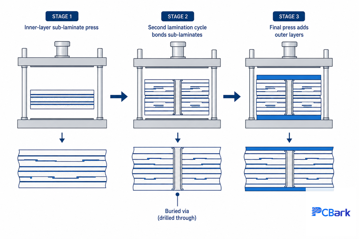
In the pcb manufacturing process building an otherwise conventional multilayer is done in a single lamination step, all the layers become fused to each other under heat and pressure at once. That breaks down as soon as the design of a 16 to 24 layer build starts to include buried or blind vias, which it usually, though not always does at that layer count.
NASA’s own microvia engineering documentation frames it precisely: “an alternative approach to pin-parallel composite building is a sequential buildup of the layers, which allows buried vias.”
The constraint is on the architecture of the via and the density of the routing, not simply on the layer count – it’s technically possible to construct a 16 to 24 layer design with only through vias in a lower number of cycles.
When this level of signal-layers on high pin-count devices starts happening, you’ll frequently run into vias (that means that the norm is sequential lamination), to one degree or another. A Reddit engineer who does HDI fabrication stated this fairly plainly: “having to use sequential laminations is a big cost adder. Laser drilling from outer to next layer isn’t a big cost adder.
Stacked vias are a big cost adder and greatly limit who can build the board.” Here’s the way that it work out in a 20 layer board: you can make up two sub-laminate’s, and drill through-vias between the sub-laminates and glue the two sub-laminates together. For each new structure with buried vias you’ll add one new lamination step.
Materials must withstand cycles of heat and pressure and not come apart, or “delaminate.” JPL and NASA Glenn Research Center obtained actual process parameters for lamination – a hot-and-pressure oven (an autoclave) operating at 300°C and 100 psi for an hour a cycle – and performed thermal cycles from -125°C to 100°C (no delamination occurred for 21 cycles). Laminate and prepreg materials are qualified to IPC-4101E, which includes specifications for glass transition temperature (Tg), the coefficient of thermal expansion (both X and Z axis) and resistance to CAF (conductive anodic filament) growth, factors that can make or break whether materials make it through more than one pressing cycle.
⚠️ Important
It is not good enough to be material spec’d CAF-resistant on paper alone. A published root-cause analysis from Chang Gung University in Applied Sciences followed a real PCB burn-out on a public transport communication board that was fabricated with CAF-resistant laminate and still failed via CAF formation. The real issue turned out to be mechanical microcracks introduced by the fabrication’s V-cut de-panelization process — which let moisture in and defeated the laminate’s CAF resistance entirely.
Bob Willis, a highly-quoted expert in SMT & assembly defects, makes an analogous statement about delamination: Delamination is often erroneously blamed entirely on moisture – in fact the mechanism is generally caused by weak inter-layer bonds and/or contamination introduced during lamination – and the moisture just exploits the weakened adhesion.
“PCB delamination can be subtle or obvious. It is caused by expansion of moisture in the PCB laminate, but that may not be the root cause… poor bonding during manufacturing of the multilayer board or some form of contamination may result in poor adhesion on inner layers, permitting moisture to accumulate.”
Bob Willis, SMT & Assembly Defect Analyst, Printed Circuit Design & Fab
FICT Ltd’s 2026 patent addresses this general class of problem directly: offsetting the conductive-paste via position away from directly above the core through-hole so that resin thermal expansion during lamination bonding doesn’t apply destructive stress to the via, improving long-term reliability for server-motherboard and high-speed interposer applications.
Controlled Impedance and Signal Integrity Across Deep Stackups
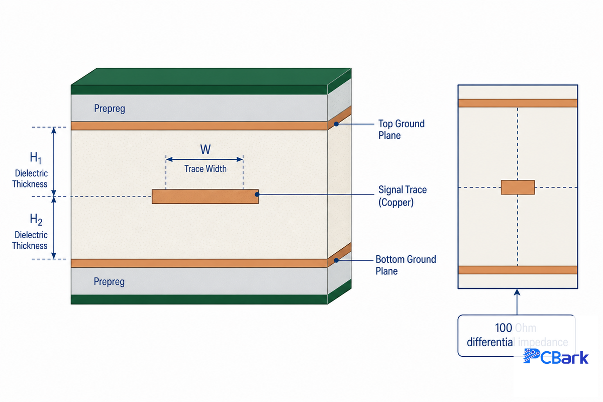
Maintaining the same impedance through 16-24 layers is all about the control of dielectric thickness and repetition of reference-plane location through all the lamination steps – it’s the same physics as on a 4-layer board, just with more chances for the deviation to accumulate. Normal fabrication performance holds impedance within 10% and up to 5-7% on an up-charge version with more refined dielectric thickness and tested traces. IPC-6012F’s Amendment 1 (which was rolled into the present version) provides for thinner internal conductor thicknesses than the table previously did.
This offers greater impedance control in the multilayer stacks by reducing variation as copper layer thicknesses decrease.
📐 Engineering Note
On a real 24-layer design targeting 100 Ω differential impedance, the achieved result was 99.76 Ω, a 0.24 Ω error, well inside a ±10% (±10 Ω) standard tolerance band and close to premium-tier ±5-7% capability. Specify your target impedance and tolerance explicitly in fabrication notes, and request impedance-coupon test data back, don’t assume “controlled impedance” on a purchase order translates to a specific number without verification.
For controlled-impedance orders, PCBark provide one TDR (time-domain reflectometry) verification report per board, together with 100% flying probe test and AOI for every inner core, before lamination – it isn’t a sampling method. Every core, before final lamination – that’s the verification layer required for any impedance tolerance on a data-sheet. Stub length off a via is one of the bigger uncontrolled variables in a deep stackup’s impedance and insertion-loss budget, which is exactly the problem a recent backdrilling patent addresses directly by re-positioning the via relative to the drill to hold a tighter zero-clearance tolerance.
Blind, Buried, and Stacked Microvia Structures: The Via-Type-to-Lamination-Cycle Cost Map
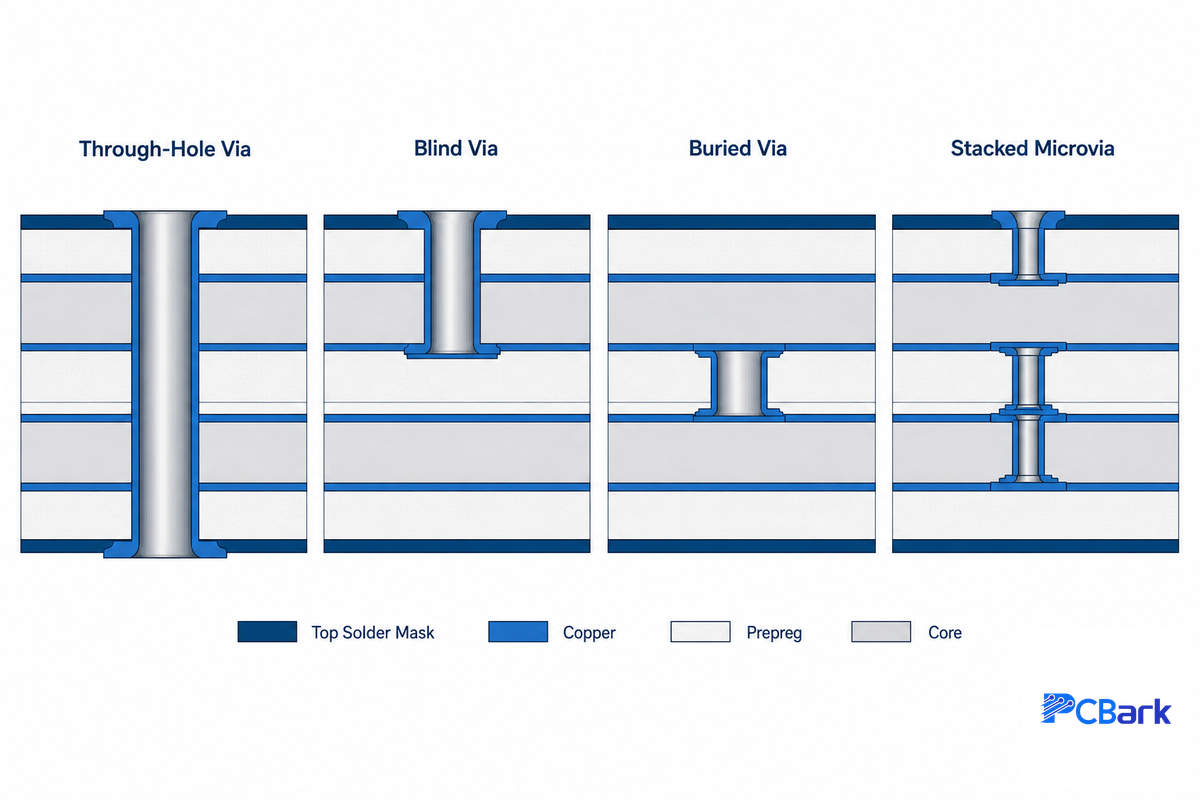
Each type of via you define on a 16-24 layer board comes with a real cost and a lamination cycle impact – not an abstract “advanced feature” line item. Per IPC-2226A, a microvia is defined as having a diameter less than 0.15mm and aspect ratio up to about 1:1 (though often more like 0.8:1 in practice, like a 4-mil dielectric with a 5-mil drill). Blind and buried via structures generally add 10-30% to fabrication cost depending on the number of HDI layers and the density of microvias – and one real-world Xilinx application note on a 16-layer PCIe stackup illustrated the cost further: each new type of blind or buried via introduced on a given board adds about 30% to the cost of lamination.
| Via Type | Added Lamination Passes | Relative Cost Impact |
|---|---|---|
| Through-hole only | Single cycle | Baseline |
| Single blind via type | +1 sub-laminate bond | ~+30% (per via type added) |
| Buried via | +1 sub-laminate bond | ~+10-30% (HDI-layer/density dependent) |
| Stacked microvias | Multiple sequential passes | Largest cost adder — also narrows which fabricators can build it |
The underlying physical constraint for all of this is the aspect ratio that the laser drilling system is capable of drilling with adequate yield. AtlasPCB’s yield impact bands translate this tradeoff clearly: aspect ratios below 6:1 have minimal yield impact; 8:1 to 10:1 require optimization; and above 12:1 you’re into special equipment territory with reduced yields and associated pricing penalties. This happens because the plating ‘throwing power’ – or how much copper actually deposits in the middle of a drilled barrel compared to the surface – goes from 80-90% at 5:1 to 40-55% at 12:1.
💡 Pro Tip
IPC-6012F now provides specific limits for microvia dimples and protrusions instead of relying on the vague “as agreed between user and supplier.” Limits are specified as no more than 25µm depression on holes ≤0.15mm (50µm on larger holes) and no more than 25µm protrusion on filled/capped microvias intended for assembly soldering. Ask your fabricator to confirm their metrology program measures against this table, not just a verbal agreement.
Is a High-Layer-Count Board the Same as HDI?
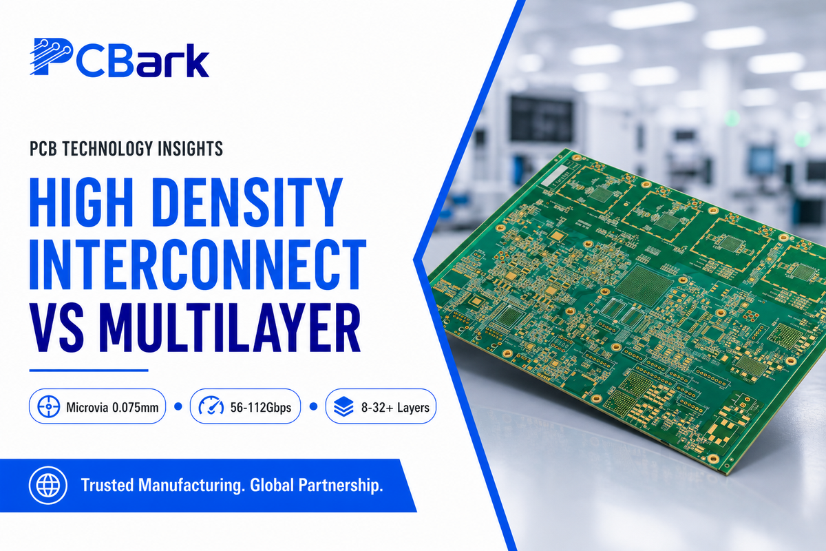
Not automatically. Layer count and HDI (High Density Interconnect) construction are two independent, high-density-routing design axes that may intersect but don’t overlap entirely. Standard, through-via stackup construction typically uses minimum via sizes in the range of 0.2mm for layer counts in the 4-8 range that support around 10Gbps.
HDI constructions employ minimum via sizes of 0.075mm or less on typically 8-32+ layer boards that can support 56-112Gbps and beyond, and the same lamination-reliability discipline covered in a NASA Glenn Research Center flex-circuit lamination study applies just as much to a microvia-heavy HDI build as it does to a conventional through-via stackup. So a 16-24 layer board could be built as a conventional, all-through-via stackup, as a full HDI design, or anywhere in between-layer count alone isn’t definitive. For an in-depth side-by-side comparison, see our HDI vs. multilayer PCB comparison.
✔ When Conventional Multilayer Fits
- Through-hole vias suffice for your routing density
- Signal speeds stay in the ~10 Gbps range
- Cost sensitivity outweighs board-size constraints
⚠ When HDI-Hybrid Is Worth It
- High-pin-count BGA fanout demands microvia routing
- Signal speeds exceed ~25 Gbps/lane
- Replacing an 18-layer conventional board with a 10-layer HDI-equivalent cut cost roughly in half in one documented case
A truly counter-intuitive, to state plainly, statement worth mentioning is that more layers isn’t necessarily better. The three separate, independent PCB manufacturers – unrelated in any way to each other – make the exact same point. One expresses it about as starkly as any engineering blog that we could find for this research: “layer count is the symptom you bill for. Stack-up is the disease you actually have.” Another makes it a direct comparison: “a well-designed 4-layer board can outperform a poorly designed 6-layer board. The key is appropriate layer assignment and proper stack-up configuration, not just layer count.” A third simply states it as a common misunderstanding that fabricators are frequently told: “a common misconception is that more layers automatically translate to higher quality… the real determinant of PCB quality lies in rigorous design principles, precise process control, and reliable manufacturing practices.” While we couldn’t find an academic or standards-body source that specifically makes this claim, the fact that independent commercial fabricators say this is certainly a notable point to know even without higher-tier validation.
Where 16-24 Layer Boards Actually Get Used

The primary uses for 16-24 layer boards are server/HPC backplanes, networking switch fabrics, and aerospace/defense avionics, due to high-pin-count BGAs and multi-domain power distribution that require the separate signal/power/ground planes that a lower layer count simply can’t provide, according to industry segmentation data for 2024-2025.
Servers, HPC, and AI Accelerator Platforms
In the server/high-performance computing (HPC) market for PCBs, which totaled $18 billion in 2023 according to industry market researcher Prismark, more than 60% of these PCBs are 18-24 layer, and the segment is projected to grow at over 20% year-over-year to $25 billion by 2025. On a typical 24-layer server board, a significant allocation of layers is designated to power and ground, usually amounting to around 8 power and 4 ground planes, in order to efficiently manage signal integrity. AI server motherboards, meanwhile, are now trending higher, increasing from 14 layers in 2019 to an average of 18-22 layers by 2024, with products like Dell’s PowerEdge line using 20-layer boards to facilitate AI inference. In related analyses of the AI mainboard market (also referencing the Prismark research but through a different trade publication), a common approach is a hybrid construction that typically uses 20-30 conventional multi-layer core boards, complemented by 2-8 high-density interconnect (HDI) layers for the most signal-intensive regions; this has driven the HDI PCB market category to achieve growth of 17.8% in 2024, outperforming all other PCB types.
Aerospace and Defense
The same factor – high component fan-out – drove avionics and defense electronics towards this range, with an added layer on top of it: IPC-6012FS, a Space and Military Avionics Applications Addendum to IPC-6012F, which serves as the Class 3 quality barrier these boards were built to withstand — a bar comparable in spirit to NASA’s own soldered-connection workmanship standard for flight hardware. A high pin count BGA fanout was one of the primary causes that led many design to be categorized in this range, according to an Electronic Design article by engineer Brendon McHugh: “one of the biggest drivers for large layer stackup is high-pin-count ball grid arrays (BGAs), where special consideration must be given to the ‘breakout’ or ‘fanout’ of the traces.” For more detail about aerospace design criteria, look to our aerospace PCB design guide.
Key takeaway: not every application benefit from maximum layer count. As one practicing fabricator put it in an AMA, high layer count and copper thickness bring “no advantage, really” for applications that don’t need the routing density — “would you rather carry an iPhone or an iHuge.” Match the layer count to the routing and power-domain requirement, not the other way around.
Fabricator Verification: The Fabricator Verification Scorecard

A quote sheet tells you what a fabricator says they can build, it doesn’t tell you whether they can verify it after the fact, and for 16-24 layer boards with blind/buried vias, verification is where reliability risk actually hides — the same class of latent microvia-plating risk documented in NASA’s microvia reliability engineering report. IPC itself has issued a direct industry warning on this point: traditional inspection techniques are no longer an effective quality-assurance tool for detecting microvia-to-target plating failures, meaning a board can pass initial acceptance testing and still fail later during reflow, environmental stress screening, or field service.
The Fabricator Verification Scorecard
| Do they cite PCQR²/IPC-9151-equivalent capability data at your exact layer count? | Ask for the panel report |
| Do they issue TDR impedance verification reports per board, not per lot sample? | Per-board = higher confidence |
| Do they run 100% e-test (flying probe) and AOI on every inner core before final lamination? | Catches inner-layer defects pre-bond |
| Do they X-ray BGA joints and cross-section/micro-section inner copper on production lots? | Catches latent microvia/plating defects IPC flags as invisible to surface inspection |
| Have you disclosed every blind/buried via and via-in-pad requirement up front, along with complete Gerber and drill files? | Changes lamination sequencing and quote |
| Do they offer turnkey PCB assembly (SMT/THT) with functional test if your board feeds a backplane or module? | Avoids a fab/assembly handoff gap |
This is precisely what PCBark’s own process is built to answer: IPC-6012 Class 2/3 workmanship, TDR-verified impedance reporting on controlled-impedance orders, 100% flying-probe e-test and AOI on every inner core, X-ray on BGA joints, and cross-section/micro-section inspection of inner copper, as part of turnkey EMS service spanning DFM through SMT/THT assembly and functional test, under ISO 9001:2015. Ask any fabricator you’re evaluating the same six questions above; the answers tell you more than a capability chart.
Cost and Lead Time Realities for 16-24 Layer Boards

PCB fabrication costs for this layer range come in different units depending on the source and they don’t quite align to a single figure – which is useful information in itself. One fabricator’s published pricing puts a 24-layer prototype (1-10 pieces) at $800-2,500 per board, with production-volume FR4 builds running $150-400 per board, with premium low-loss materials adding 40-60%. A separately published, independent percentage-based framework indicates that each additional copper layer adds roughly 10-20% to fabrication cost on top of a basic 2-layer board, with a 6-layer board almost doubling the price of a 2-layer of equivalent size – and blind/buried vias or via-in-pad structures add an additional 30-50% on top depending on layer count. Both suggest the same general direction – that cost is growing faster than layers – but neither is a replacement for a project specific quote. Part of that cost curve is the extra press cycle every via-structure change demands, which is exactly the cost driver a 2026 laminated-substrate patent tries to engineer around by reducing the stress a given via places on surrounding material during bonding.
📐 Engineering Note
Lead times have shifted substantially since 2024. A fabricator-side report indicates typical lead times for complex multilayer boards ran 4-6 weeks prior to the AI infrastructure demand surge, but complex multilayer AI-server board lead times are now extending out 12-20 weeks as of 2025-2026 and fabrication costs are up 20-40% on some items in 2025 compared to 2024. Broader electronics supply reporting suggests a general increase in component and PCB material cost pressures industry-wide in 2024 but doesn’t break down by exact week counts. Work with your specific fabricator for up-to-date lead times as this isn’t a guaranteed quote.
Estimates for global PCB market size are varied enough among market research firms that offering any single figure implies more precision than any single report truly has. A market research report compiled from Korean and Taiwanese trade press and customs data via TrendForce shows a market of roughly $92 billion in 2025 with growth of 28-35% driven by AI; another independent market research firm estimated $74 billion in 2025 growing to $130 billion in 2034; a third estimated the market at $80 billion in 2025 with a 5.2% CAGR through 2032. Treat any specific market size or CAGR figure you see – including these – as directional and not authoritative.
Where the Layer Count Is Heading: AI/ML, 800G Networking, and HPC

AI accelerator and 800G-networking demand is pulling sequential-lamination fabrication capacity tight industry-wide, copper-clad laminate import prices reached $20,728 per ton in March 2026, up 74.5% from a year earlier, per TrendForce’s compilation of Korean and Taiwanese trade press and customs data, the first time import levels have exceeded $20,000/ton since records began in 2000.
For anyone planning a 16-24 layer board on a 2026 timeline, the practical implication is straightforward: lock in fabricator capacity earlier in the design cycle, not after tape-out, the material and process capacity this layer range depends on is under real, dated pressure, not a hypothetical future risk.
It’s not a one-off report. TrendForce’s own research arm states that NVIDIA’s newest generation of Rubin GPUs are “reshape the demand for advanced substrate and PCB material,” carrying substantially more layers than their predecessors. Separate trade reports citing Prismark research corroborate AI mainboards have moved into hybrid 20-30-plus-layer-plus-HDI designs and that the HDI category grew a whopping 17.8% in 2024-the highest of any PCB class. Meanwhile, a networking-focused analyst firm corroborates the 800G/1.6T transition driving the “networking” part of this trend and projects the market for AI scale-out Ethernet to exceed $100B by 2030. Fabricator-side engineering is already responding to that pull: a 2026-filed backdrilling patent aimed at server-motherboard and high-speed interposer applications is one concrete sign of where via-structure engineering is headed as layer counts climb past today’s 16-24 range.
💡 Pro Tip
The nuance worth planning around is that the bleeding edge of AI accelerator demand has already moved beyond 16-24 layer PCBs. NVIDIA’s Blackwell GB300 architecture reportedly uses 28-34 layers of PCB, and the next generation platform, Vera Rubin (expected in H2 2026), is forecast to push beyond 40 layers, bringing the average layer count of AI server PCBs up from 18 in 2023 to 32 in 2025 – a 78% jump in just two years. Read that again: 16-24 layers is where current production capacity is being pulled up from by AI demand, not the cap of where AI demand will drive layer count. If your platform is anything beyond 2026, expect “high layer count” to mean more than 24.
Frequently Asked Questions
Q: How much does a 16-24 layer PCB cost?
View Answer
Pricing will vary significantly with via structure, material grade, and quantity, rather than layer count alone. According to one fabricator’s price list for prototypes (1-10 pieces), 24-layer boards range from $800 to $2,500, while production-quantity boards utilizing standard FR4 cost $150-400 per piece. This will increase another 40-60% with the addition of high-performance, low-loss materials. Generic percentage-based estimates indicate each additional layer will increase price by approximately 10-20% over a two-layer baseline; the inclusion of blind or buried via technology could add an additional 30-50%. As always, treat this as an estimate – consult with your fabricator for a project-specific quote.
Q: What is the minimum hole size for a 24 layer PCB?
View Answer
Minimum standard hole sizes for mechanically drilled through holes typically begin at 0.15mm (approx. 6 mils), with a limit on aspect ratios commonly in the range of 10:1 to 12:1 (depending on the specific equipment used by the fabricator). Laser-drilled microvias go smaller — IPC-2226A defines them as under 0.15mm in diameter with a maximum aspect ratio around 1:1 (commonly 0.8:1 in practice, such as a 4-mil pad with a 5-mil drill). Your fabricator’s capability will determine your practical minimum.
Q: Can blind and buried vias be used together in a 16-24 layer board?
View Answer
It is, especially at this layer count with complex vias, though each new type of via requires its own press step and compounds both cost and the number of fabricators capable of building it. A real-world application note from Xilinx describing the cost increase of a 16-layer PCIe board with several blind and buried via types noted each additional type of via contributed about 30% to the lamination cost. Plan your via structure early with your fabricator and fully disclose any blind, buried, or via-in-pad requirements up front.
Q: How thick is a 24 layer PCB?
View Answer
One reference design was a published 24-layer stackup with 10 signal layers and roughly 160 mils of total thickness. However, total thickness can vary greatly based on copper thickness, selection of dielectric, and via construction; always verify against your specific stackup.
Q: Is a 16-24 layer board the same as an HDI board?
View Answer
No – the number of layers and whether a board is HDI constructed are two independent design decisions, though often overlap at this layer range. A conventional through-via stackup can be designed to up to 24 layers with no HDI features at all. Conversely, a HDI-hybrid design employs microvias (which is less than or equal to 0.15mm in diameter, per IPC-2226A) in order to increase routing density and signal speed to much higher than a conventional via construction (which typically maxes out around 10Gbps vs. 56-112 Gbps for advanced HDI). Whether your 16-24 layer design requires HDI will be determined by the pin density of your BGA(s) and the speeds you are looking to run, not just by the layer count. See our HDI vs. multilayer for more.
Q: How long does it take to manufacture a 16-24 layer PCB?
View Answer
The supply chain has changed a lot since 2024. Previously, a 4-6 week turn was standard for advanced multilayer PCBs, but as the demand for advanced AI hardware ramped up in 2025 and 2026, leading times on high-layer count designs have stretched out to as long as 12-20 weeks due to the competition for limited fabrication and material resources. Double check current lead times directly with your fab.
Do you need a complete, end-to-end 16-24 layer board design and build solution?
Why We Write This
PCBark specializes in the manufacturing and end-to-end validation of 16-24 layer boards for telecom, server backplane, and aerospace customers through our integrated EMS offering. This article shares the key questions on stackup, lamination, and testing that we pose to all customers seeking a controlled-impedance quotation. Updated July 2026. Reviewed by the PCBark Technical Team.
References & Sources
- NASA-STD-8739.1B, Workmanship Standard for Polymeric Application on Electronic Assemblies — NASA
- NASA-STD-8739.3, Soldered Electrical Connections — NASA
- NASA Glenn Research Center / JPL flex-circuit lamination reliability study — NASA
- NASA Microvia Reliability Engineering Report — NASA
- 24-Layer PCB Stackup Optimization Case Study (2025) — Missouri University of Science and Technology, Scholars’ Mine
- Root-Cause Analysis of PCB CAF Failure via De-Panelization Microcracks — Applied Sciences (MDPI), Chang Gung University
- IPC-4101E, Specification for Base Materials for Rigid and Multilayer Printed Boards — IPC / Global Electronics Association
- Advanced Microvia and HDI Design Technical Resource (E18&S25-1) — IPC / Global Electronics Association
- IPC-6012F Qualification and Performance Specification for Rigid Printed Boards, Official Release — IPC / Global Electronics Association
- IPC Industry Warning: Printed Board Microvia Reliability — IPC / Global Electronics Association
- US12557217B2, Zero Clearance Backdrilled Printed Circuit Boards — Nokia Solutions and Networks Oy (Google Patents)
- US20250374420A1, Laminated Substrate and Method of Manufacturing Laminated Substrate — FICT Ltd (Google Patents)
- Controlling Radiated EMI Through PCB Stack-Up — Rick Hartley, EE Times
- PCB Delamination Root Causes — Bob Willis, Printed Circuit Design & Fab
- AI Demand Tightens CCL Supply, Drives Advance Orders and Price Hikes — TrendForce
- Inside the AI Hardware Boom: Servers, Substrates, and Advanced Packaging — I-Connect007
- In the AI Era, Ethernet Set to Surge — 650 Group
Related Articles
- 8-12 Layer PCB Design Guide, sequential lamination and via structure at one tier down
- 6-Layer PCB Guide, stackup fundamentals before you scale up
- 4-Layer PCB Guide, the baseline stackup every higher layer count builds on
- Aerospace PCB Design Guide, qualification requirements for avionics-grade boards
- Multilayer PCB Hub, comparing 4 through 42 layer options
- HDI vs. Multilayer PCB, when microvia construction is worth it