Get in touch with PCBark Company


By: The PCBark Technical Team at Shenzhen Linghangda Technology. Reviewed By Our Engineering Team.
An 8-12 layer PCB is a multilayer circuit board dense enough that it breaks the mold of a simple, inexpensive 4-layer board, forcing the use of sequential lamination, controlled impedance, and blind or buried vias just to function reliably. This guide explores the scenarios in which you actually need a printed circuit board design with so many layers, how to best architect its stackup, what via structure works for your routing density, and what a fabricator can (and should) verify before signing off on a quote. If you’ve already made that call and just need a fabrication partner, our 8-12 layer PCB fabrication page covers capabilities and quoting directly.
8-12
Layer range covered
30-40%
Cost step per added layer pair
±5-10%
Typical impedance tolerance
2023-09-28
IPC-6012 Revision F release date
When Do You Actually Need 8, 10, or 12 Layers?
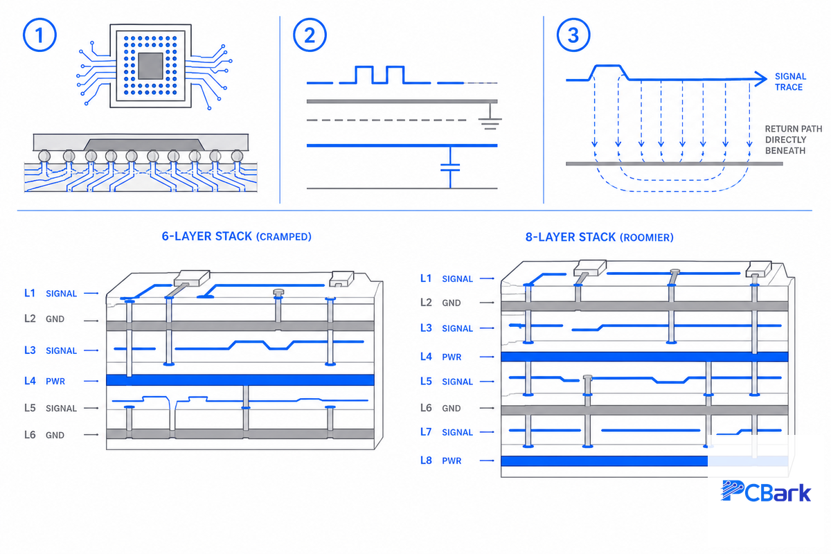
Most designers move to 8 or more layers not to look sophisticated, but because a project needs more routing channels, power planes, or EMC and signal-integrity headroom than 6 layers can physically provide. A well-known EMC rule of thumb from engineer Henry Ott holds that 8 layers is the minimum needed to meet five classical EMC objectives at once: a dedicated ground reference, a dedicated power reference, enough signal layers, controlled trace impedance, and an unbroken shielding barrier.
The Three Key Factors Behind an 8-12 Layer Board Designs transition to 8 or more layers in practice for three key reasons: The density of the routing traces under a BGA: Many high-pin-count BGAs necessitate an 8-layer stackup to effectively route signals under the device, particularly on a 6-layer design where there isn’t enough space without resorting to many expensive vias. Lack of room for dedicated reference planes: Designs with complex high-speed buses or numerous independent power supplies require dedicated reference planes; an 8-layer stackup offers sufficient space to allocate dedicated ground and power references. Signal integrity issues: High-speed interfaces like DDR4/DDR5 and PCIe Gen4/5 require the trace return current to be immediately beneath the signal trace. An 8-layer stackup ensures adequate signal layers and reference planes to support this requirement with controlled trace impedance. Examples in the industry illustrate these points: an 8-layer stack for a 6.6 kW bidirectional EV on-board charger dedicated an entire layer as a ground return plane to cancel out flux on power traces, and a GaN dual-stacked bridge converter used an 8-layer stackup specifically to achieve better coupling of the transformer primary and secondary windings and reduce AC resistance-this used 4oz copper for inner layers and 2oz for outer layers. Aerospace and industrial-control PCB manufacturing operates on the same principle: a design that contains more separate power supplies, complex mixed-signal circuitry, or a greater number of breakout pins for BGA and FPGA components beyond what a lower layer count can physically handle is often pushed to an 8, 10, or 12-layer stack by necessity, rather than by choice, and that manufacturing process reality doesn’t change whether you’re building a custom pcb prototype or a production run.
What Is an 8-Layer PCB (and How Is It Different from a 12-Layer Board)?
An 8-layer pcb is a multilayer board built with eight conductive copper layers — typically a mix of signal layers and dedicated ground or power planes — sufficient to provide the routing channels and reference planes a moderate-to-high-speed digital or mixed-signal design needs. A 12-layer board extends the same idea with more signal layers and often more dedicated power-plane splits for separate voltage domains.
As discussed in the academic via-modeling source cited below, a 12-layer board also has more head room for differential pairs to transition between layers without getting trapped in a single layer. “12 is just a bigger 8” doesn’t quite tell the full story, though: a 12-layer board has capacity for many more independent high-speed nets and power domains than an 8-layer board before conflicts arise among layer-to-layer via pads and power/ground planes.
💡 Selection Logic
If your BGA breakout requires more routing channels than your 6-layer board’s inner layers can supply, and you’ve got two or more different power domains that need their own reference plane, now is the time for an 8-layer or greater stack-up-not just because you have a fast chip. One Electronics StackExchange discussion highlights the issue from the opposite angle, stating that an 8-layer board is a great option “both for performance and development time. No downsides other than cost,” while several experienced engineers in the same thread caution against choosing a stack-up based solely on the hope of a “safety margin” before ensuring that you’ve fully exhausted other routing control options, since every pair of added layers costs 30-40% of the board’s base price.
Stackup Architecture for 8, 10, and 12 Layer Boards
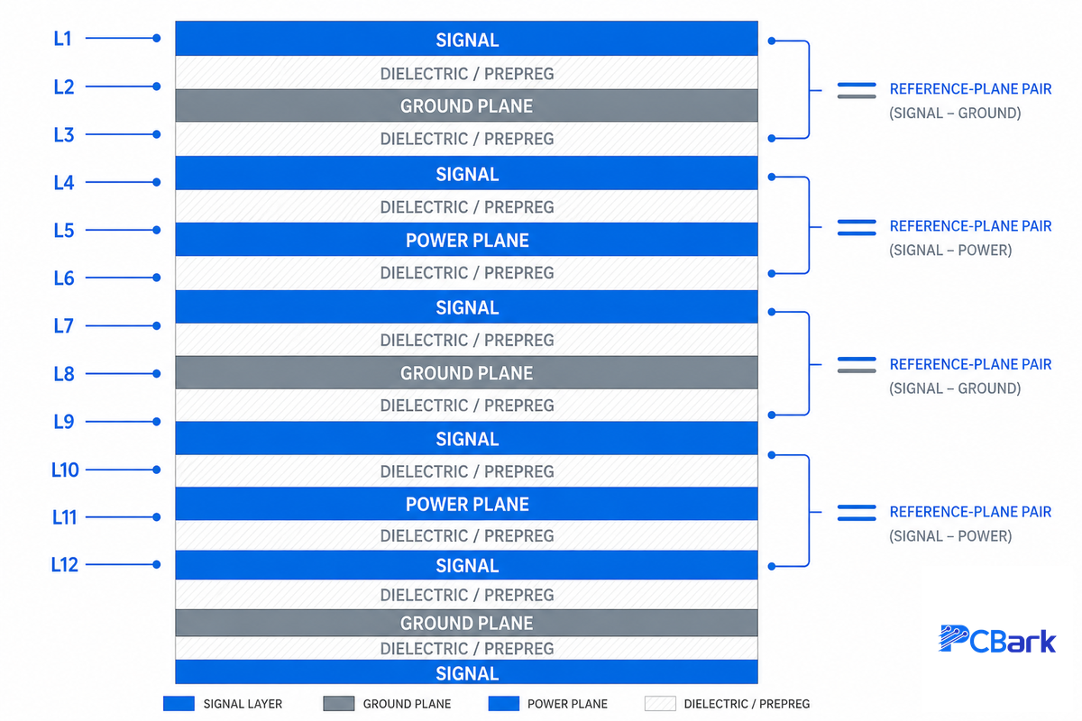
This is The 8-12 Layer Stackup Blueprint: at the core of good stackup design in any workable 8- or 12-layer stack is ensuring each signal layer is in direct contact with either a ground plane or a power reference plane. Symmetrical ordering (a mirrored image of layers of copper thickness and prepreg/dielectric spacing with regard to the center of the stack) also helps prevent warpage during the lamination process. Determining the number of layers is only step one; after deciding how many layers you need, the next major design choice is how to stack multiple layers together rather than treating each one as one layer in isolation. The internal layers are the workhorses, and one 8-layer stack-up designed for a planar transformer in a GaN power converter, for example, uses 4 oz copper on six internal layers to combat the skin-effect resistance and 2 oz on the top and bottom layers to enable smaller trace spacings. Regarding EMI, EMC consultant and EDN contributor Kenneth Wyatt published an 8-layer example where the power and ground reference planes are spaced just 4 mils apart (much closer than the 20-40 mils of a basic 4-layer pcb), with vias placed about every 1 cm along the edge of the board stitching together all of the ground reference planes; this spacing can be tightened to 1-3 mils for improved EMI control and crosstalk reduction between neighboring signal layers. One federally-funded NSF-archived study on a 12-layer through-hole via design makes a related structural point: the number and placement of vias is itself a stack-up decision, not an afterthought layered on top of a finished architecture, because via placement interacts directly with which internal layers can carry return current cleanly.
How Thick Is an 8-Layer vs. 12-Layer PCB?
There’s no single universal number, but as a general range, 8-layer boards fall between approximately 1.57mm and 2.36mm depending on copper weight and dielectric choice, while 12-layer boards tend to fall between about 1.6mm and 2.4mm — which is why vendor pages vary by a tenth of a millimeter or two on this.
Anything thinner often implies thinning the dielectric itself, bringing you closer to HDI and microvias-more on that below. If you’ve searched for a 4-layer PCB stackup, a 6-layer PCB stackup, or a 10 layer PCB stackup example before landing here, the same logic scales up: how thick doesn’t just mean “how thick is the thing,” but “how was this actually constructed.”
| Layer Count | Typical Structure | Typical Thickness | When It Fits |
|---|---|---|---|
| 8-layer | 2-3 signal layers, dedicated GND/PWR planes, symmetric build | ~1.57-2.36mm | Moderate-density BGA, 1-2 high-speed buses (DDR4, single PCIe lane group) |
| 10-layer | 4+ signal layers, split power domains | ~1.6-2.2mm | Multiple voltage rails, moderate BGA pin count, blind vias becoming common |
| 12-layer | 5+ signal layers, multiple ground/power plane pairs | ~1.6-2.4mm | Dense BGA/FPGA routing, several concurrent high-speed buses, mixed analog/digital |
Blind, Buried, and Through-Hole Vias, Choosing the Right Structure
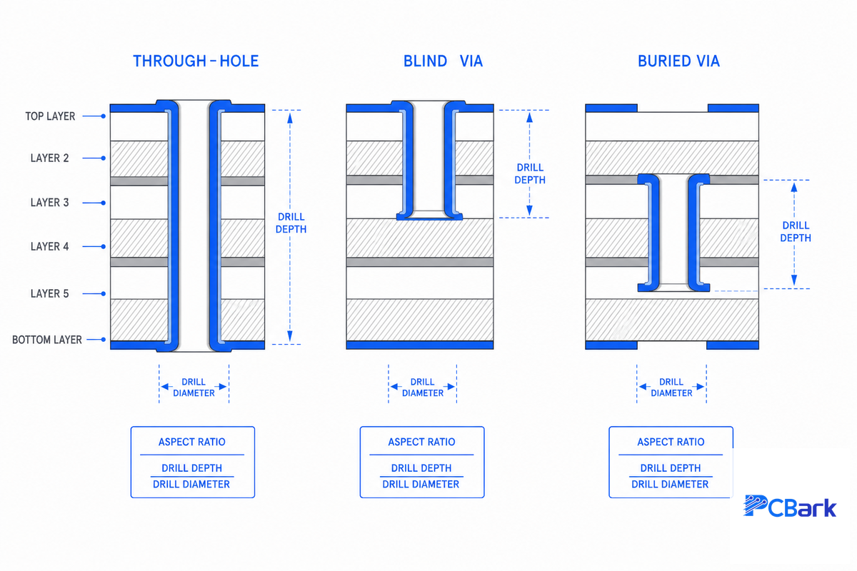
This is The Via Structure Compass: assume that through-hole will be the default on a multi-layer PCB until your design is actually space-constrained by BGA breakout and it’s impossible to route with more through-holes without adding at least 2 additional layers-why? Every blind/buried via requires an additional sequential lamination step. “It’s also quite possible to design a PCB that’s literally impossible to fabricate because no sequence of drill cycles and sequential laminations will produce all the through holes,” as one particularly insightful poster put it on Electronics StackExchange when working an IPC Type III HDI design. Practitioners have anecdotally reported blind holes become more common place as you step from 8 to 10 layers; 8-layers often get by just fine with through-holes alone as the cost of sequential lamination doesn’t often pay off until you run out of space for through-holes in a dense board. IPC-2226A, the sectional HDI design standard, formally classifies this progression into Types I through VI: Type I uses only through vias connecting the outer layers, Type II adds buried vias inside the core, and Type III (two or more HDI layers) is where blind and buried vias can appear together with through vias. A NASA NEPP reliability report gives a genuinely useful rule of thumb for when that progression is actually necessary: conventional multilayer boards routing 1.0-1.27mm-pitch area-array packages can use plated-through holes without microvias at all, while finer-pitch packages are what actually force the move to microvias — which lines up closely with the roughly 0.8-1.0mm threshold discussed later in this guide. The same NASA data is also a useful caution against over-miniaturizing: in their test set, 2-mil (about 50µm) microvias failed after 100 thermal cycles while larger via structures in the same test did not, and a separate University of Maryland reliability dissertation found that a microvia with a 16% conical void retained only 1.4% of the fatigue life of a void-free one — smaller isn’t automatically better once you’re into microvia territory.
This is your aspect ratio (AR); this is the one real gate that determines whether or not a hole is manufacturable. and as a general matter, actual manufacturers don’t fully agree on what the “real” AR limit is: Sources referring to IPC-A-600G will often specify a buried via limit of 1:10, but will call 1:12 special. At least one German fabricator’s own design-rule page specifies a tighter 1:8. Blind holes are a bit more consistent, with sources placing the limit between 1:1 and a “target” of 0.75:1. You can’t guess; your best bet is to get this in writing from your specific manufacturer, as it depends more on the capability than on an industry-wide constant.
| Via Type | Aspect Ratio (Drill:Depth) | Typical Diameter | When It’s Used |
|---|---|---|---|
| Through-hole (standard) | up to ~10:1 | ≥0.2mm | Default for 8-12 layer boards with moderate routing density |
| Through-hole (reliability-critical) | ~8:1 max | ≥0.25mm | High-vibration or thermal-cycling applications where plating integrity matters more than density |
| Blind via (mechanical, standard) | 1:1 | 200-300µm | BGA breakout that a through-hole can’t clear without extra layers |
| Blind via (mechanical, special production) | 1:1.2 | ~150µm | Denser breakout, higher process cost |
| Blind via (laser microvia) | 1:1 (0.75:1 ideal) | ~100µm | HDI-adjacent designs, sub-0.8mm BGA pitch |
| Buried via (mechanical, standard) | 1:8 to 1:10* | 200-400µm | Internal-layer-only connections on 10-12 layer boards |
| Buried via (special production) | 1:12 | ~330µm pad | Maximum internal routing density, highest cost tier |
| Controlled-depth drill | n/a (depth-limited) | Varies | Only when a genuine controlled-impedance requirement forces it; fabricators bill this as a premium step |
| Via-in-pad | Fabricator-specific, filled/plated | Component-pad-sized | Tight BGA pitch where routing must escape directly under the component |
*Buried-via aspect-ratio ceilings genuinely disagree across real fabricators (1:8 to 1:12 depending on the source) — treat this column as a starting point for your own fabricator’s written spec, not a fixed industry constant.
Via Selection Checklist
- Start with through holes. Blind and buried vias are your friend only when the BGAs are so dense you’d need 2+ additional layers to route with only through holes.
- Make sure to get your chosen manufacturer’s aspect ratio limits in writing; 1:8, 1:10, and 1:12 have all appeared on manufacturer documentation for standard features.
- When you can avoid them, don’t layer blind (L1-L3) and buried (L2-L4) via structures in the same part of your stackup; doing so increases manufacturing costs.
- Only specify controlled-depth drilling if it’s absolutely necessary; manufacturers treat this as an added difficulty and will bill you for it.
Controlled Impedance and Signal Integrity at 8+ Layers
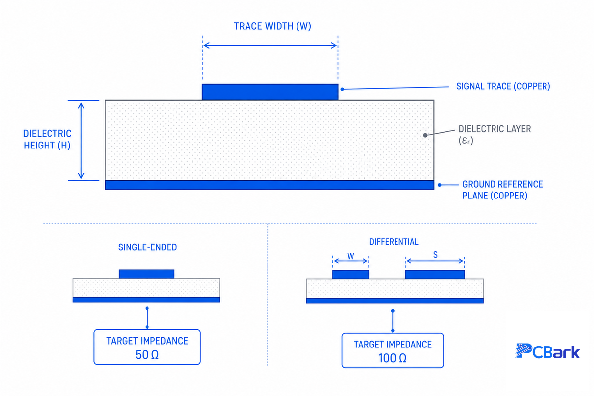
As soon as a board has DDR4/DDR5, PCIe or some other GHz-class signaling on it, “impedance” ceases to be a background thought and is now a specification that you give to your fabricator instead of something you pray just magically works. There was a worked example from one fabricator where they were building an 8-layer DDR4/PCIe Gen4/USB 3.0 controller board and they had targeted 50 ohms single ended and 90-100 ohms differential and measured their TDR (time-domain reflectometry) at 100 ohms tolerance within ±5% on that specific board. This is just one useful example of what’s possible, not necessarily what you’ll always achieve because the actual tolerance on impedance is influenced by your specific stack-up and your fabricator’s process control. Incidentally, the microvia-specific impedance tolerance is most commonly said to be within ±10%, so the tolerance you should generally expect on impedance is around ±5-10%, again depending on via structure and stack, not just a single value. One published MIT Power Electronics Research Group study on a GaN dual-stacked bridge converter is a useful real-world data point on the same theme: they deliberately used an 8-layer stackup, with heavier 4oz copper on inner layers, specifically to control coupling and AC resistance well enough to hit their impedance and efficiency targets — the layer count and copper weight were themselves impedance-control decisions, not just routing-capacity decisions.
“The slight asymmetry in the stackup created by dissimilarities in thickness of different laminates… could also induce warpage into the stackup if the build is not balanced”, and differential thermal expansion due to differing coefficients of thermal expansion (CTE) of dissimilar dielectric materials “could lead to differential expansion of the stackup and thus cause a propensity for barrel cracking and delamination under thermal cycles.”
Zachariah Peterson, IEEE member, writing in Altium’s design resources
There are other electrical concerns at this layer count than just impedance, as well – generic design rules defined in IPC-2221 such as conductor clearance/creepage by voltage, and the conductive-anodic-filament (CAF) resistance, are equally important considerations on a mixed high-voltage/high-speed board even if they rarely receive the attention in vendor marketing material that impedance does. Both the choice of dielectric material (standard FR4 vs. a lower-loss epoxy-glass or PTFE-based laminate) and power distribution design (how many discrete power supplies your board will need to reference cleanly) influence the calculation of this same impedance control, not just trace width. For our own impedance controlled orders, we provide a TDR verification report free as standard, not an additional option; this is because a stack-up can look perfect on paper but still fail to hit the desired impedance when real-world dielectric variation and etch tolerance are accounted for, and the only way to know for sure is to actually measure the completed product.
Sequential Lamination, Why 8-12 Layer Boards Cost and Take Longer to Build
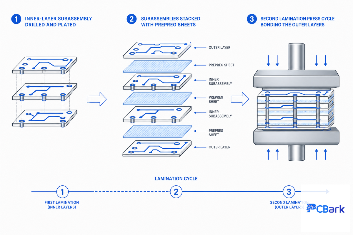
4-layer boards are generally built up in one pass as part of a normal PCB production run. But an 8 or 12 layer board generally isn’t – instead, subassemblies of inner layers are drilled and plated (e.g., 1-4 and 5-8 on an 8-layer) then laminated together on the second pass. This is The Sequential Lamination Cost Curve: cost rises not so much with the number of layers but with the number of lamination cycles, and indeed many PCB fab houses estimate that per-layer-pair costs rise about 30-40% with an extra lamination cycle.
Again, that’s just an industry rule of thumb to be taken with a pinch of salt, and get a real per-layer cost from your own chosen fabricator – that added-process cost is what needs budgeting for. And as with so many other processes, extra processes means extra lead time. A rule of thumb that one fab house used to apply was three extra working days per process step added, and a lamination cycle certainly adds a process step. What actually matters isn’t the cost line item itself — it’s a fabricator that under-quotes lamination cycles to win a bid, then discovers mid-run that a misaligned sub-assembly requires a costly rework. PCBark’s own production line archives lamination-cycle and alignment data per lot for a minimum of five years precisely because that traceability is what lets a fabricator catch a drifting process before it becomes a field failure, not after. One process-chemistry patent from Atotech, a major lamination and plating materials supplier, underscores the same cost driver from the materials side: the plating and lamination chemistry used at each cycle is itself an engineered cost variable, not a fixed commodity input.
However, the number of lamination cycles is a stack-up-planning variable, not a function of layer count per se: One HDI design rules document indicates that “a 10-layer HDI board could potentially be fabricated using only 3 lamination steps instead of 5, provided careful planning was applied as to which layers should be built in each substack. Also, a cost-modeling effort by the IPC/SMTA (SavanSys Solutions and Ormet circuits) studied a “real board” in the form of a 10-layer mobile application and a 28-layer server application comparing the traditional 5/10 lamination steps vs. Z-interconnect approach.
In both real-board instances, the Z-interconnect construction slightly outperformed traditional 5/10 lamination approaches with respect to the modeled total cost. (The authors warn that overhead cost and profit margin vary widely among fabrication factories, and thus, they caution that the model should be viewed only as a general illustration of potential costs.)
8-12 Layer Sequential Build vs. HDI Any-Layer, Which Should You Choose?

There’s no universal winner: HDI carries a per-layer cost premium for its blind and buried via structures, but it can meet the same routing density in fewer layers — so the honest comparison is total-board cost, not layer-for-layer cost. A 6-layer HDI board doing the same job as a 10-layer sequential board can end up cheaper overall, even though HDI processing itself costs more per layer.
IEEE EMC literature makes the same point at the single-layer level: you pay a premium to include blind or buried vias you’d otherwise have no way of placing within your trace density. An HDI manufacturer states it plainly on its FAQ page: the extra cost of HDI processing “is offset on the total-board basis by fewer board layers” once a BGA pitch gets near the 0.8mm limit.
If you’re near that pitch edge, do yourself a favor and run the comparison on a dollar basis rather than assuming either construction method wins by default-a dedicated HDI vs. multilayer PCB comparison is worth reading before you commit.
| BGA / Component Pitch | Recommended Approach | Why |
|---|---|---|
| ≥1.0mm pitch, moderate density | Standard 8-12 layer sequential build | Through-hole/limited blind vias route the fanout without microvias; lower total cost at this density |
| 0.8-1.0mm pitch, dense fanout | Evaluate both; run the cost comparison | This is the threshold band where HDI’s layer-reduction savings start to offset its higher per-layer cost |
| <0.8mm pitch, dense BGA/FPGA | HDI any-layer / microvia construction | Standard through-hole physically cannot fan out this pitch without excessive layer count; HDI is often cost-competitive here too, not just technically necessary |
Stepping Up from 4 or 6 Layers, What Actually Changes at 8-12
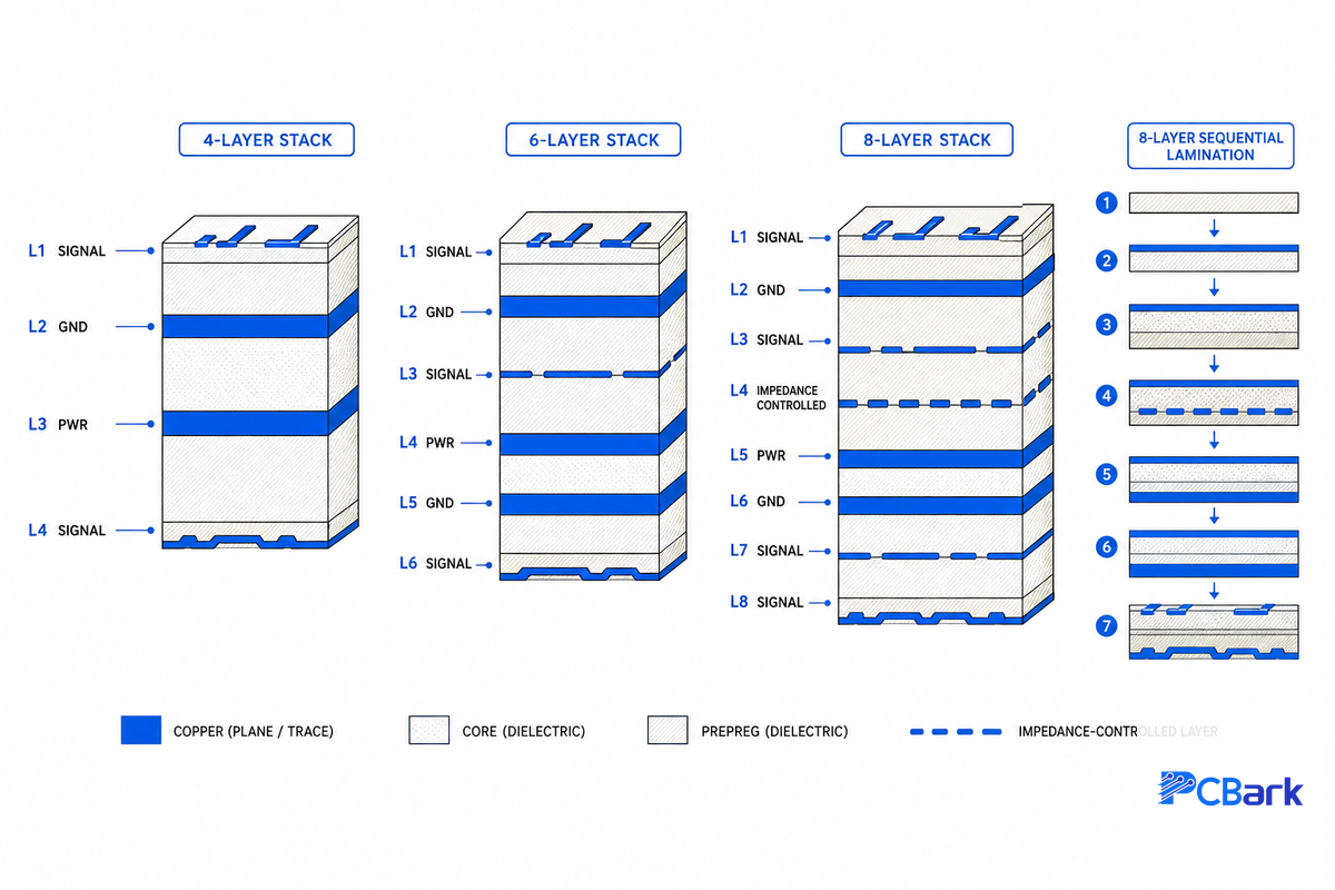
Jump to an 8-layer board from six layers, four layers, or (heavens forbid) a two-layer pcb or double-layer pcb, and it’s no longer the case of just adding more of the same thing. JLCPCB’s PCB blog recently had an excellent piece worth memorizing: as you step from 4 layers to 6, then 8 or 10 layer, then 12-layer PCB layers, your costs won’t climb steadily; rather, the “step” can jump sharply or even regress temporarily for specific run sizes at specific layer counts. Mid-range 6-layer production runs can, for reasons of fab flow and throughput mismatch, cost more than 4- or 8-layer boards. The engineering differences between 4/6 and 8-12 layers? Forcing reference planes, default sequential lamination (not single shot), and the ubiquity of blind/buried vias. Suddenly, your board is an “engineered stackup” requiring proper discipline, and the mistake we see most often at this transition is a design team that reuses their 4-layer DFM checklist on an 8-12 layer board and only discovers the gap when a batch fails electrical test. PCBark’s IPC-6012 Class 2/3 workmanship and 100% flying-probe test on every order exist specifically to catch that gap before it reaches a customer, not after a field return. One multilayer construction patent from TTM Technologies, one of the larger PCB manufacturers, reflects the same reality at the manufacturer level: scaling a construction method up past a handful of layers is treated as its own engineering problem worth patenting, not a simple repeat of the 4/6-layer process.
Cost, Lead Time, and What Actually Drives the Price at This Layer Range

If you’re searching for 8 12 layer pcb price or 8 12 layer pcb cost benchmarks, the honest answer is that per-board cost varies drastically by volume and region – a hobby-level 8 layer prototype off the offshore Fab comes in at about $7 a board, with a 2 week turn time, whereas a 10k piece order of a 10 layer board cost $50 a board in the States vs $25 in China, as reported by various individuals in the field (see Electronics StackExchange, Reddit, etc.) Fabricators offering what they’re calling ‘standard capabilities’ typically consider 0-12 layers within their standard turn time range (same day to 5 days), with 8-layers most often costing 7-10 days, compared to 5-7 for 6-layers and 3-5 for 4-layer, while layers beyond 12, or involving any blind and/or buried impedance, are generally lumped in a custom/advanced category and have anywhere from same-day to 4-week lead times. The biggest factors driving the cost, in rough order of magnitude, are: layer count and number of lamination cycles, the latter adding ~30-40% to the board cost per lamination pair, type of via structure (blind and buried require an extra processing step beyond a standard plated through-hole), copper weight, and volume, as a small prototype order is forced to pay a large portion of a fabricator’s fixed costs in each unit, a price that mostly vanishes when purchasing in large quantities, which is why a rapid-turn high-speed PCB prototype and a 10,000 unit production run of the exact same 8-12 layer PCB stackup would have such different per-board costs. A costly mistake we see buyers make is chasing the lowest quoted per-board price without checking whether that quote actually includes 100% electrical test or is a sampled-inspection price with hidden risk baked in. PCBark quotes 48-72 hour prototype turnaround with no minimum order quantity, because the years of process discipline behind that turnaround — not a discount on inspection — is what actually controls cost at this layer range. One patented multilayer PCB construction method illustrates why: process steps that reduce lamination cycles or simplify via formation don’t just affect manufacturability, they directly change the cost and lead-time math discussed above.
What to Verify Before You Approve an 8-12 Layer Fabricator
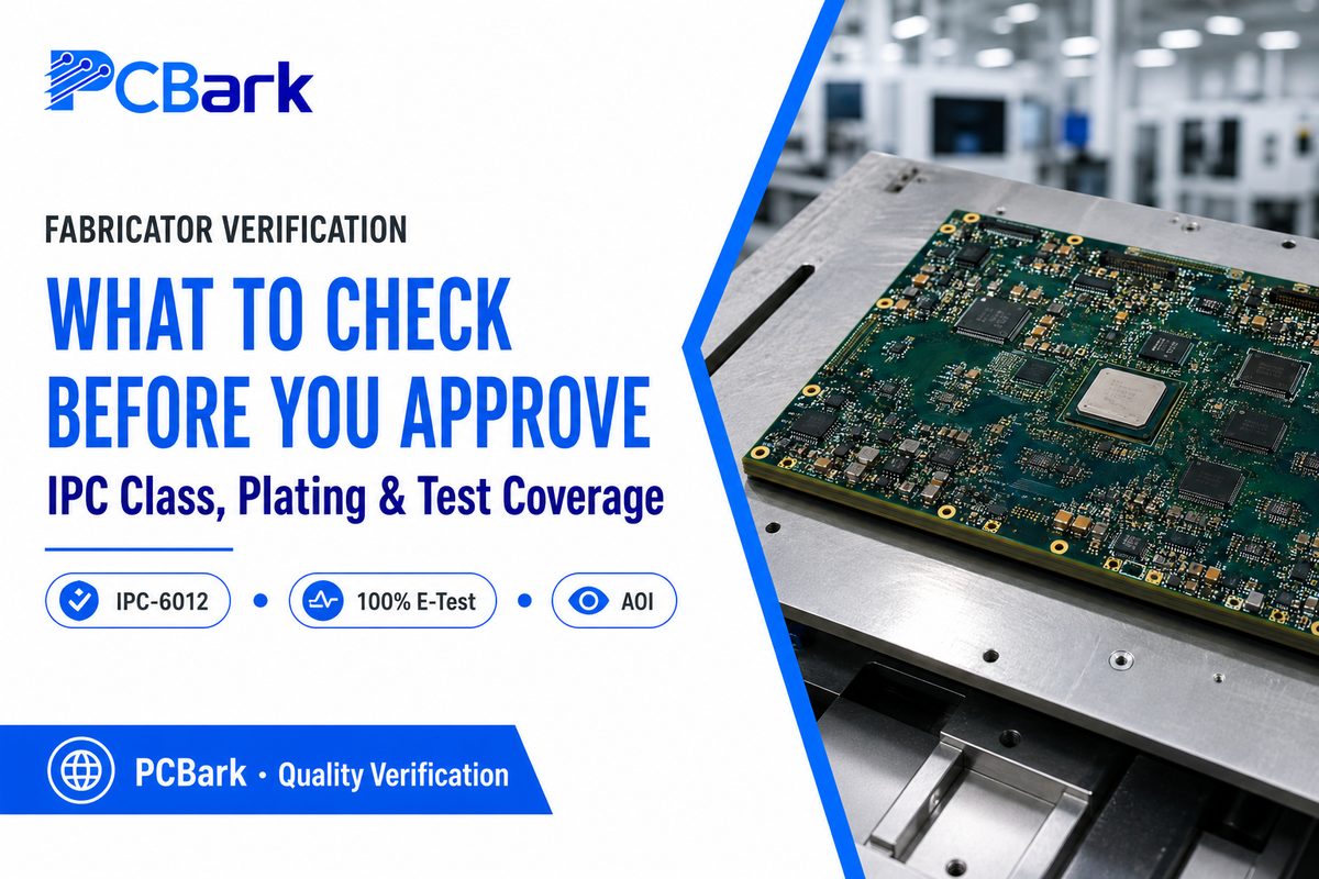
The Fabricator Verification Protocol below is the checklist we wish we’d had on the buying side of a printed circuit board order, not the selling side. IPC-6012 (Rigid Printed Circuit Board Qualification and Performance Specification, current version Revision F) sets minimum copper plating per class: Class 1/2 needs an average of 20 microns with an 18-micron minimum, while Class 3 needs an average of 25 microns with a 20-micron minimum.
Make sure to ask what class your fab actually qualifies for, and ask to see plating-thickness verification records if it matters for your application. Rev F also introduces three classes of cavity structures, plus a Class 3 annular-ring and via-wall void tolerance of 5% of the void area-worth checking if your pcb layouts assumed a different minimum void allowance. A properly-built multilayer printed circuit board at a specified class level lets you compare two fabricators’ pcb technology directly rather than just taking their word for it, and that matters even more on a complex multilayer design, where the additional cost of getting it wrong compounds across every lamination cycle.
Fabricator Verification Checklist
- Which IPC-6012 class (1, 2 or 3) does the fab qualify for and have proof to demonstrate this capability?
- If they promise controlled-impedance traces, do they provide an actual time-domain-reflection report, or only a design-time simulation?
- Is the 100% electrical test flying-probe and are inner layers visually inspected by an Automated Optical Inspection (AOI) system, or is testing sampled?
- Are BGAs x-rayed, and is the annular ring / via-wall verified through cross-sectioning and microscopic examination?
- What’s the length of time the fab retains test data and process information for a lot? (This can be useful when investigating field failures that occur much later).
With our own 8-12 layer orders, this isn’t a marketing checklist – it’s our standard process: IPC-6012 Class 2/3 workmanship, 100% electrical test (flying probe) plus AOI on every inner core, X-ray inspection on BGA joints, cross-section/micro-section analysis on inner copper, and a TDR impedance verification report on controlled-impedance orders, with process and test data stored for a minimum of five years per lot. We’d also include a single dimension that’s easy to forget at quote time: acceptance testing shouldn’t end with “passes electrical test” – for higher-reliability applications, ask whether your fabricator’s quality system carries through design-review flowdown and documented test-coupon retention, not just final-board inspection, as that’s the difference between catching a process drift after a single bad batch vs. after a field failure. A DFM review before fabrication begins is the least-cost place to identify most of these issues.
Industry Outlook, Where Multilayer PCB Design Is Heading

The most concrete near-term change for 8-12 layer designers isn’t a market-growth figure – it’s a standards update that already took place. IPC-6012 Revision F, issued September 28, 2023, is validated as the current governing revision by IPC’s own standards store, and based on one Class-3 fabricator’s published clause-by-clause reading of the update, it nudged minimum dielectric spacing guidance to more appropriately fit denser modern stack-ups (translating from a 90µm-class default toward a tighter ~65µm figure for designs issued after 2023-12-31) – regard the precise micron figures as that fabricator’s technical interpretation rather than a quote from the (paywalled) standard itself, and verify the current clause with your fabricator before designing to it. If your design library or your fabricator’s default design rules still reference the earlier Revision E assumptions, this should be flagged now rather than experienced as a delay or a rejected design during DFM review on your next 8-12 layer order — that’s a preventable mistake, not a surprise. PCBark tracks IPC revision changes as part of our own DFM review process precisely because a design built to an outdated assumption is a risk that shows up at the worst possible time: after tooling is committed. IPC’s own release notes encompass Revision F more broadly – addressing rigid boards, multilayer plated-through-hole boards, buried/blind vias, and microvia reliability – so this isn’t a niche HDI-only change; it affects standard multilayer PTH construction as well.
Underlying that specific update, the broader market context (directional only, not the load-bearing point here) is ongoing growth in both the overall PCB market and, at a noticeably faster rate, the HDI segment specifically – market-research firms including Grand View Research and Mordor Intelligence estimated overall PCB market growth in the 4.8-5.8% CAGR range through the early 2030s, with HDI-specific segment growth estimated meaningfully higher. Practically, that means the HDI-vs-sequential cost comparison discussed above is likely to continue shifting in HDI’s favor over time as that segment matures, which is another reason to actually run the comparison for your own pitch and volume instead of defaulting to whichever construction method your existing fabricator happens to focus on. One construction patent from DDI Global, an HDI-focused manufacturer, is a concrete signal of where that investment is headed: fabricators are actively patenting finer-pitch, higher-density construction methods rather than treating the current generation of stack-ups as a stable end state.
Frequently Asked Questions
Q: Are 12-Layer PCBs Always HDI Boards?
View Answer
No. An 8 or 12 layer board can be fabricated with a standard sequential-lamination stack-up using only through-hole or limited blind vias, with no HDI microvia structure at all — this is the most common approach when component pitches are at or above about 1mm and component density is such that finer structures are not necessitated. HDI approaches (microvias, any-layer build-up) only come into play when BGAs or component pitches dip below about 0.8mm and you simply cannot route the signal out of the device on a standard through-hole stack without adding a number of layers to the stack-up. Layer count and HDI construction are distinct but related design decisions.
Q: Is Standard FR4 Suitable for an 8-12 Layer PCB Project?
View Answer
For the vast majority of 8-12 layer boards running at moderate speed, the best board is a standard FR4 stack; layer count itself doesn’t necessitate a change in dielectric material. The change is driven by frequency and signal-loss requirements; once you are routing signals well above a few GHz, the dielectric loss (Df) of FR4 becomes a limiting factor, and you must move to a low-loss dielectric material (Rogers, PTFE-based, etc.) irrespective of stack-up. Keep layer count and material selection separate; each decision is driven by a different set of constraints.
Q: What’s the Single Biggest Manufacturing Challenge at This Layer Range?
View Answer
Lamination cycle yield loss. Each sequential lamination pass carries a small, but real, probability of misalignment and delamination. The multiple lamination cycles of an 8 or 12 layer stack-up mean that the risk compounds-which is precisely why many fabricators move dense boards into single-lamination techniques (like Z-interconnect, any-layer HDI, etc.), where layer density permits and lamination risk can be eliminated, even if single-lamination itself is more expensive on a per-layer basis. The most powerful design tool for mitigating this risk is stackup symmetry (equal thickness and copper weight of internal layers about the centerline); non-stackup stacks are significantly more susceptible to warpage during lamination cycles.
Q: Why Does Cost Increase So Sharply Between a 6-Layer and an 8-12 Layer Board?
View Answer
Mostly sequential lamination and via complexity, not the raw copper. Each added pair of layers costs about 30% to 40% more than the base stackup, due to the extra lamination cycles, stricter alignment tolerances, and, potentially, blind/buried via fabrication; not simply because there’s “more copper.”
Q: What Should I Check Before Approving a Fabricator for an 8-12 Layer Board?
View Answer
Minimum: confirm which IPC-6012 class (2 or 3) they actually possess qualifications and plating thickness records for, ask whether their controlled-impedance designs ship with TDR test reports or merely with pre-layout simulations, determine if testing of internal cores is 100% and is AOI, rather than sampled, find out whether their BGA-joints are x-rayed, and their inner copper is sectioned to confirm the size of the annular rings, inquire how long their process/test data are archived (this is your tool if/when a board fails in the field), etc. See the full checklist above for everything you should look for; this is the abridged version.
Q: Can High-Speed Signals Like DDR or PCIe Be Routed Reliably on an 8-Layer Board?
View Answer
Yes, if the evidence of at least one fabricator-published worked example – an 8-layer stack-up carrying DDR4, PCIe Gen4, and USB 3.0 simultaneously reported 700 mV of DDR4 eye height at 1.6 GHz, insertion loss below 10 dB at 8 GHz, with TDR-verified 100-ohm differential impedance to within ±5% for that particular board (don’t take the exact numbers as gospel on your design, obviously) – then an 8-layer is sufficient. But that’s with an adequately engineered stack-up (dedicated reference planes on the top & bottom, and behind every internal high-speed signal layer, backdrilled vias to remove stub length). An 8-layer pcb board lacking those requirements can fail these same signals where a good one will work perfectly, and so that stack-up architecture discussion in the prior section is far more important to high-speed reliability than just layer count. This is exactly what a prototype pcb run should catch before you sign the PO.
References & Sources
- Micromachines (PMC/NIH) — 8-layer PCB stack-up for an EV on-board charger flux-canceling design
- NSF Public Access Repository — 12-layer through-hole via design-parameter study
- MIT Power Electronics Research Group (IEEE JESTPE preprint) — 8-layer stack-up for a GaN dual-stacked bridge converter
- IPC official standards store — IPC-6012 Revision F and IPC-2221 Revision C current-revision confirmation
- IPC/SMTA-hosted cost-modeling paper (SavanSys Solutions & Ormet Circuits) — sequential lamination vs. Z-interconnect cost comparison
- EDN — Kenneth Wyatt, “Design PCBs for EMI, part 2: Basic stack-up”
- Altium Resources — Zachariah Peterson on hybrid stackup reliability
- IPC-2226A — Sectional design standard for HDI printed boards, Type I-VI classification
- NASA NEPP — Microvia reliability and pitch-threshold test data
- University of Maryland dissertation — Microvia void reliability quantification
- US Patent 20070124930A1 — Multilayer PCB construction method
- US Patent 10980127B2 (TTM Technologies) — Multilayer construction/scaling method
- US Patent 20220304164A1 (Atotech) — Lamination/plating process chemistry
- US Patent 8510941B2 (DDI Global) — HDI construction method
Why We Write This
We wrote this guide because in every 8-12 layer PCB blog we reviewed while researching it – including the two highest-ranking ones for this exact topic – we found exactly zero verifiable facts or claims. We didn’t see a single reference to an IPC standard, to any government or academic authority, or any impedance or aspect ratio figure that wasn’t purely self-generated and unsupported.
We manufacture 8-12 layer boards under IPC-6012 Class 2/3 discipline every day, and so this is the guide that *we* would have wanted to read before signing off on a stack-up.

![Rigid Flex PCB Design: Aerospace & Compact Devices [Guide]](https://pcbark.com/wp-content/uploads/2026/08/rigid-flex-pcb-design-featured-150x150.png)