Get in touch with PCBark Company

8-12 Layer PCB
8–12 Layer Multilayer PCB Manufacturing
Quality and a low defect rate decide most multilayer sourcing calls — not the lowest sticker price. PCBark is a multilayer PCB manufacturer that backs 8 to 12 layer boards with published specs, verifiable certifications, and 100% electrical test on every panel. You see the numbers before you commit, not after a failed batch arrives.
STANDARDS
- 100% E-Test
- No MOQ
- 16+ yrs
CERTIFICATIONS
- IATF 16949:2016
- ISO 14001:2015
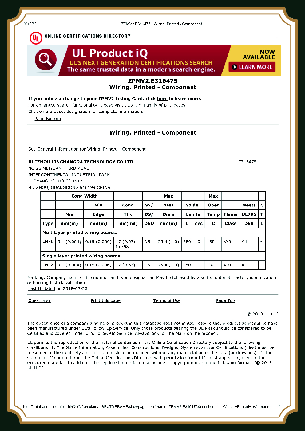
- UL Recognized · E316475
- IPC-A-600/6012 Cl 2&3
[PIC-01]
[PIC-02]
SPECIFICATIONS
- layer count (8–12 std) 4–32+
- min. line / space 0.075 mm
- controlled impedance ±5–10%
- electrical test 100%
- layer-to-layer reg. ≤75 µm
- annual capacity 500,000 m²
Why 8–12 Layer Boards Fail in Production — and How We Prevent It
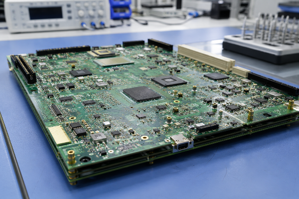
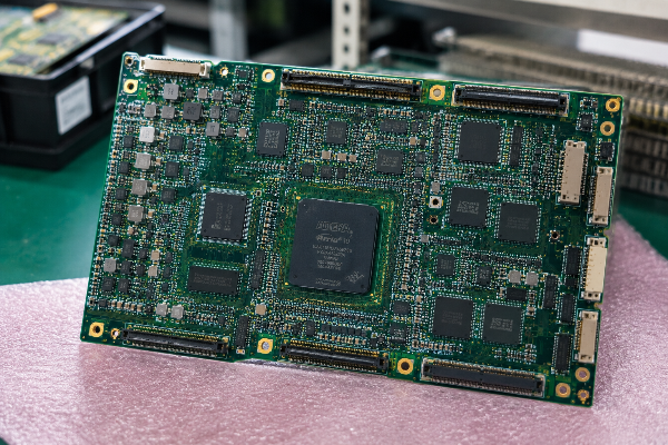
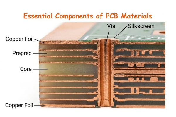
An 8–12 layer PCB — also written multi-layer PCB — is a multilayer printed circuit board with 8 to 12 conductive copper layers bonded by prepreg and cores under heat and pressure, carrying inner signal, ground, and power planes. Stacking multiple layers this way gives high-density electrical connections in a smaller footprint than two-layer boards, which is why complex designs in modern electronics rely on them. Routing different layers for signal, ground, and power also sits at the boundary between mainstream multilayer and high-layer-count work, where layer-to-layer registration and via formation get genuinely hard.
More layers is not automatically better. A poorly planned 8-layer stackup will still radiate, ring, and miss impedance targets, and a higher layer count can hide a weak design while adding cost. The right question is not “how many layers can I afford” but “which stackup hits my signal-integrity and reliability targets at the lowest total cost.”
The three failure modes we engineer against
-
01
Impedance drift is the first.
FR-4 dielectric constant shifts with frequency, so an uncontrolled stackup misses 50 Ω single-ended and 100 Ω differential targets. We hold impedance to ±5–10% and verify it with TDR before shipping.
-
02
Registration and via reliability come next.
Temperature, humidity, and drill accuracy distort alignment on every added layer, and misregistration cracks plated barrels. We hold layer-to-layer registration to ≤75 µm and back the holes with ≥20 µm barrel copper.
-
03
Invisible inner-layer faults are the costliest.
Automated optical inspection cannot see whether buried vias actually connect to internal layers — only an electrical test catches an open inner net. Every PCBark panel gets a 100% electrical test for exactly this reason.
PCBark 8–12 Layer PCB Capabilities
— Full Spec Matrix
Most multilayer quotes hide the numbers that matter, which leaves you guessing whether a fab can hit your spec — an expensive risk when a board fails at assembly. Specs stay vague for a reason: a loose “controlled impedance” claim is harder to be held to than a published ±5–10% with a line and space down to 0.075 mm, because real numbers invite accountability.
Our honest version is the full table. Every figure below comes from PCBark’s in-house process-capability sheet, and PCBark engineers each stackup against these numbers rather than a marketing range. Unlike spec-light suppliers, we publish the Standard column for most 8–12 layer work alongside the Advanced and Maximum columns, so you confirm the build against your design before you commit.
| Parameter | Standard (8–12L) | Advanced | Maximum |
|---|---|---|---|
| Layer count | 4–12 layers | 14–24 layers | 32 layers or above |
| Base material | FR-4, High-Tg FR-4 | High-Tg, halogen-free, high-speed | Rogers, Isola, Panasonic Megtron, hybrid |
| Board thickness | 0.6–2.4 mm | 0.4–4.0 mm | 0.3–6.0 mm |
| Min. line width / spacing | 0.10 / 0.10 mm | 0.075 / 0.075 mm | 0.050 / 0.050 mm |
| Outer / inner copper | 1–2 / 0.5–2 oz | 1–4 / 0.5–3 oz | 6 / 4 oz |
| Min. laser via | 0.10 mm | 0.075 mm | 0.050 mm |
| Blind & buried vias | Available | Multilayer blind/buried | Multi-step HDI stacked |
| Impedance control | ±10% | ±8% | ±5% |
| Layer-to-layer registration | ≤75 µm | ≤50 µm | ≤35 µm |
| Surface finish | HASL-LF, OSP, ENIG | ENIG, ENEPIG, Imm. Silver | ENEPIG, hard gold, selective |
| Max. finished size | 400 × 500 mm | 500 × 600 mm | 600 × 1200 mm |
| Testing | 100% electrical test | + AOI, flying probe, impedance | + TDR impedance, reliability |
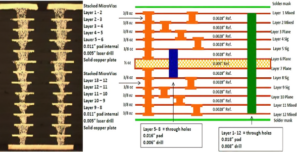
Our ±5–10% impedance window and 0.075 mm line/space track what trade-press case studies report for real 8- and 14-layer HDI builds (3–3.3 mil line/space, ±8% impedance). Published 8/14-layer HDI case studies describe the same controlled-depth drilling and filled, stacked microvias we run. The build approach is also reflected in granted process patents for copper-filled microvia reliability.
REF PATENT
USPTO US12245383B2 (2025)
| If your design needs… | Recommended build | Key spec lever |
|---|---|---|
| Standard digital, ≤1 GHz | 8-layer, FR-4 / High-Tg, ±10% | Cost-efficient, 0.10 mm line/space |
| DDR4/DDR5, BGA pitch ≤0.5 mm | 8–10 layer, High-Tg, ±8% | Dedicated planes + length matching |
| High-speed / >1 GHz RF | 10–12 layer hybrid (Rogers/FR-4) | Low-Dk material + ±5% impedance |
| Dense HDI, fine-pitch BGA | 12 layer + stacked microvia | 0.075 mm line, 0.10 mm laser via |
Not sure which build fits your net list?
Get a free stackup recommendation →Choosing Your Layer Count: 8, 10 and 12-Layer Stackup Configurations
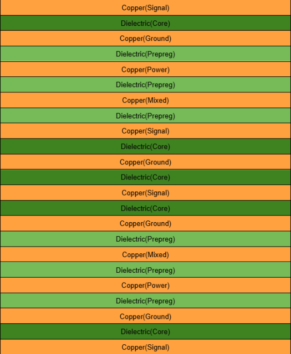
Two quotes for "an 8-layer board" are not always equal. Some shops pad the count with non-functional or balance layers, so a nominal 8-layer can carry fewer working signal and plane layers than you expect — and we will not claim that simply adding layers fixes a noise or EMI problem, because a weak stackup on 8 or 12 layers still behaves badly. Layer order is the structural reason: a signal layer belongs next to a reference plane, not just stacked higher. PCBark delivers the working arrangement up front, proven on real 8 layer pcb stackup and HDI multilayer pcb builds, so you compare like for like.
A standard 12-layer board runs around 1.6 mm as a baseline, though most 8–12 layer designs finish between 1.6 and 3.2 mm once copper weight and impedance control are factored in. Plane-to-signal ordering matters more than the raw number.
Material selection drives the high-speed builds
Standard FR-4 (dielectric constant ~4.2–4.7, loss tangent 0.017–0.025) is the right call for digital work, but it is the wrong material above roughly 1 GHz. For high-speed 10–12 layer boards we move to High-Tg laminates or Rogers RO4350B (Dk 3.48, Df 0.0037), and PCBark runs these hybrid FR-4 + Rogers stackups in-house, which keeps cost down where the signal does not need the premium layer.
[REF: INTELLECTUAL PROPERTY]
USPTO/WIPO patent WO2025029814A1 (2025) documents the low-Dk dielectric direction this class of board is moving toward.
08
8-layer
Servers, advanced ADAS, premium test gear
Sig / GND / Sig / Pwr / GND / Sig / GND / Sig
10
10-layer
High-speed designs balancing density and cost
Sig / GND / Sig / GND / Pwr / Pwr / GND / Sig / GND / Sig
12
12-layer
5G, radar, complex backplanes, high-reliability
Mixed / Plane / Sig pairs / Plane / Mixed (symmetric)
Choosing Your Layer Count: 8, 10 and 12-Layer Stackup Configurations
Two quotes for "an 8-layer board" are not always equal. Some shops pad the count with non-functional or balance layers, so a nominal 8-layer can carry fewer working signal and plane layers than you expect — and we will not claim that simply adding layers fixes a noise or EMI problem, because a weak stackup on 8 or 12 layers still behaves badly. Layer order is the structural reason: a signal layer belongs next to a reference plane, not just stacked higher. PCBark delivers the working arrangement up front, proven on real 8 layer pcb stackup and HDI multilayer pcb builds, so you compare like for like.
A standard 12-layer board runs around 1.6 mm as a baseline, though most 8–12 layer designs finish between 1.6 and 3.2 mm once copper weight and impedance control are factored in. Plane-to-signal ordering matters more than the raw number.
8-Layer Core
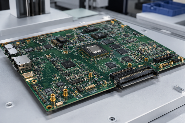
08Seq: Sig/GND/Sig/Pwr/GND/Sig/GND/Sig
Servers, advanced ADAS, premium test gear
10-Layer Density
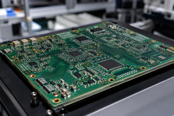
10Seq: Sig/GND/Sig/GND/Pwr/Pwr/GND/Sig/GND/Sig
High-speed designs balancing density and cost
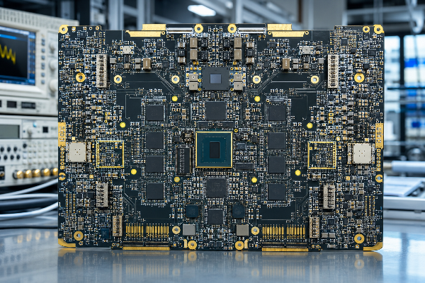
12-Layer Symm
12Seq: Mixed/Plane/Sig-pairs/Plane/Mixed
5G, radar, complex backplanes, high-reliability
Material selection drives the high-speed builds
Standard FR-4 (dielectric constant ~4.2–4.7, loss tangent 0.017–0.025) is the right call for digital work, but it is the wrong material above roughly 1 GHz. For high-speed 10–12 layer boards we move to High-Tg laminates or Rogers RO4350B (Dk 3.48, Df 0.0037), and PCBark runs these hybrid FR-4 + Rogers stackups in-house, which keeps cost down where the signal does not need the premium layer. USPTO/WIPO patent WO2025029814A1 (2025) documents the low-Dk dielectric direction this class of board is moving toward.
PCBark vs Typical Multilayer Suppliers — A Spec Comparison
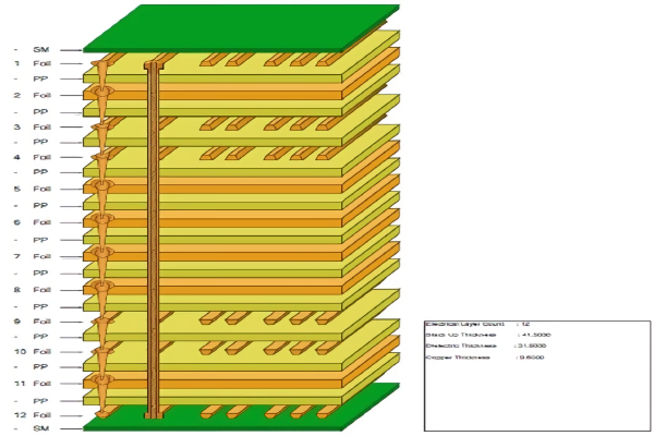
Most multilayer landing pages claim "controlled impedance" and "high reliability" with no number behind either. We take the opposite approach. The table compares what a buyer can actually verify, using the same parameters across the row, and our copper-filled blind/buried-via process follows the approach documented in USPTO patent US20220304164A1.
| What a buyer checks | Typical "spec-light" supplier | PCBark Verification |
|---|---|---|
| Impedance tolerance | "controlled impedance" (no %) | ±5–10%, TDR-verified |
| Min. line / space published | Not stated | 0.10 mm std, 0.075 mm advanced |
| Electrical test coverage | Unstated / sample | 100% electrical test |
| Internal-via verification | AOI only (cannot see buried vias) | E-test + X-ray + metallographic lab |
| Equipment transparency | Photo gallery, no models | 27 CNC drills, LDI imaging, named lines |
| Quality certification | "ISO 9001" (often unverifiable) | IATF 16949 + ISO 14001 + UL (verifiable) |
Statement of Reliability
That fifth row is the one buyers feel most. Generic ISO 9001 reassures no one when, as one engineer put it, the company name on the invoice "changes multiple times a year." A current, certification-body-traceable IATF 16949 record answers the real question: can this fab prove it, not just claim it.
Want this comparison against your current supplier's data sheet?
Request a custom comparison
Inside Our Factory: Equipment and Quality Control
You cannot judge a multilayer fab from a stock photo of a cleanroom, and the risk of getting it wrong is real — the 25% reject batch described earlier shipped because nobody could see the inner-layer fault. PCBark resolves that with the equipment behind the multilayer pcb manufacturing process, so here is what actually produces and inspects your 8–12 layer boards, by process step. Unlike the unlabeled photo galleries you will see elsewhere, every line below has a model, a maker, and a count, whereas a spec-light shop lists none.
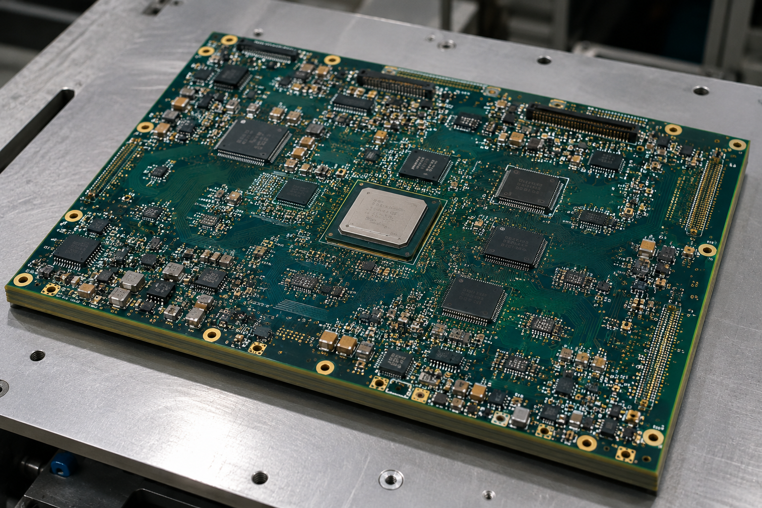
Drilling
27 CNC drilling machines, including German Schmoll and Taiwan Tongtai systems, for tight positional tolerance on dense via fields.
Imaging
LDI (laser direct imaging) exposure plus auto-align LED exposure, which holds fine-line registration far better than film on inner layers.
Plating
dedicated pattern-plating, PTH electroless copper, and vertical continuous plating (EVCP) lines for even barrel copper.
Inspection & test
in-line and offline AOI, four flying-probe testers, X-ray, a metallographic cross-section lab, peel-strength and impedance/TDR testers.
Inside that production process, copper foil and inner-layer copper are imaged and etched, the etched cores and prepreg are stacked and bonded in a vacuum lamination press under controlled temperature and pressure, and the drilled holes go through copper plating to build the conductive path between layers. UV light images the solder mask, automatic optical inspection checks each inner layer, and a final solderability check closes the line before electrical test. Every step in the lamination process is the conductive layer count's chance to drift, so manufacturing precision here is also a checkpoint.
Our QC chain maps directly to the acceptance standards. We build and inspect to IPC-A-600 and IPC-6012 Class 2 and Class 3 — which set the numbers behind every board, such as a 20 µm (Class 2) to 25 µm (Class 3) minimum hole-wall plating and 50%-to-75% barrel fill.
IPC-6012F Class 2 vs Class 3 acceptance criteria
A board has to be built to its class from the start; you cannot upgrade Class 2 to Class 3 after the fact.
"On 8–12 layer boards, the metallographic cross-section is our truth serum. We section a coupon from every controlled-impedance lot and read the barrel copper and registration under the microscope before the panels leave the line — the electrical test tells us the net is good, the microsection tells us it will stay good."
— PCBark Fabrication Engineering Team
Applications and Recommended Stackups by Industry
Layer count follows the application, not the other way around, and PCBark maps each industry to the lowest layer count that meets its signal-integrity and reliability targets. The pairings below come from how 8–12 layer boards are actually deployed across industries from 5G to aerospace.
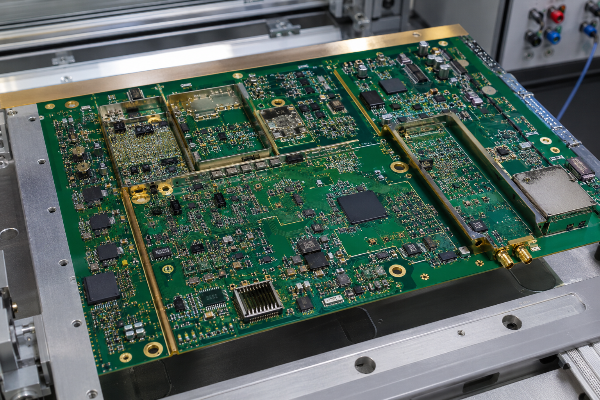
5G / telecom base stations
8–16 layersHigh-speed routing, dedicated RF planes
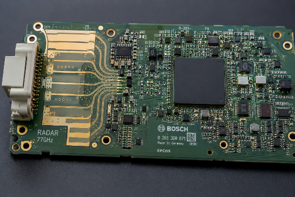
Automotive radar / ADAS
6–8 layers (+ flex)Signal integrity + IATF 16949 quality
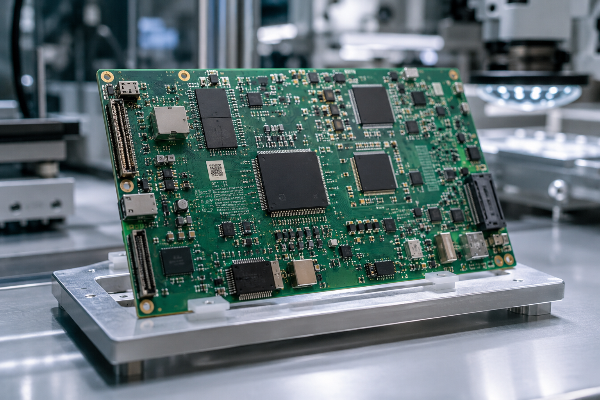
Medical imaging / implant
6–12 layersReliability, fine-pitch BGA, traceability
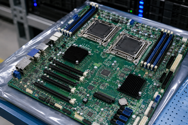
Servers / high-performance compute
8–16 layersDDR4/5 length matching, power integrity
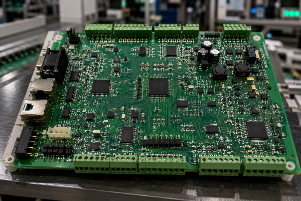
Industrial control / PLC
4–12 layersMixed digital + power, long service life
What ties these jobs together is that every one of these multilayer circuit board builds needs internal nets proven good, because none of them tolerate a field failure. That is the right call: automotive and medical buyers ask PCBark for the cross-section data, the IATF 16949 record, and 100% test coverage, not just the price. Picking the lowest layer count that still meets the target — rather than over-constraining the design — is where an experienced fab earns its place.
Tell us your application and target specs —
request a custom layer-count recommendationCertifications and Compliance
PCBark holds quality and environmental certifications that a buyer can verify with the certification body — the kind that hold up in a supplier audit, not a logo on a footer.
IATF 16949:2016
Automotive QMS · PCB manufacturing
ISO 14001:2015
Environmental management
UL Recognized
Multilayer PWB
IPC Class 2 & 3
IPC-A-600 / IPC-6012 workmanship
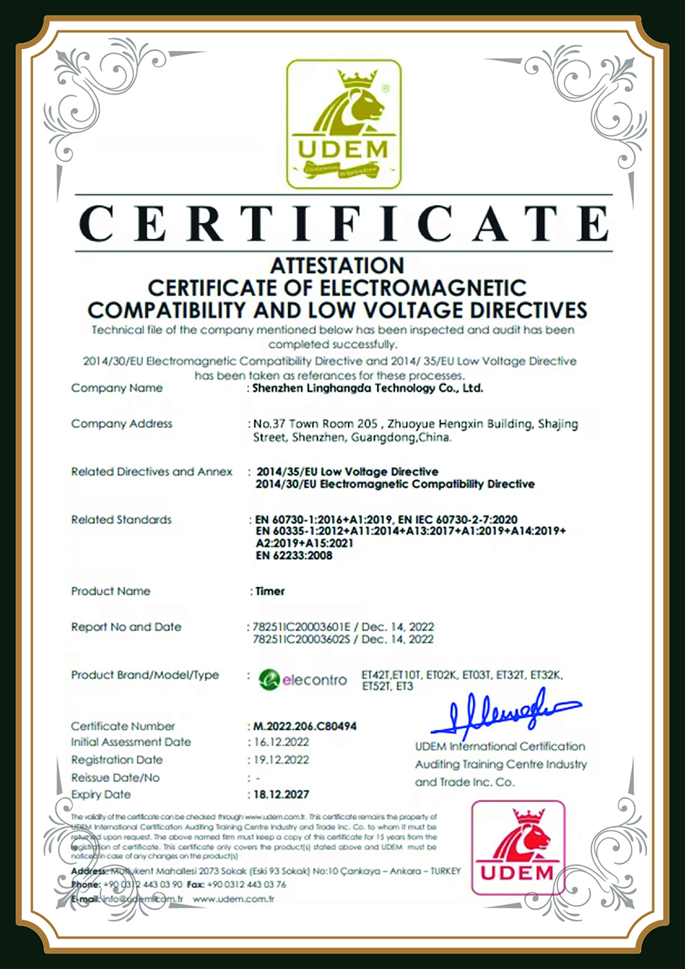
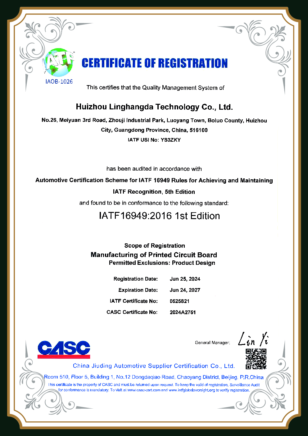




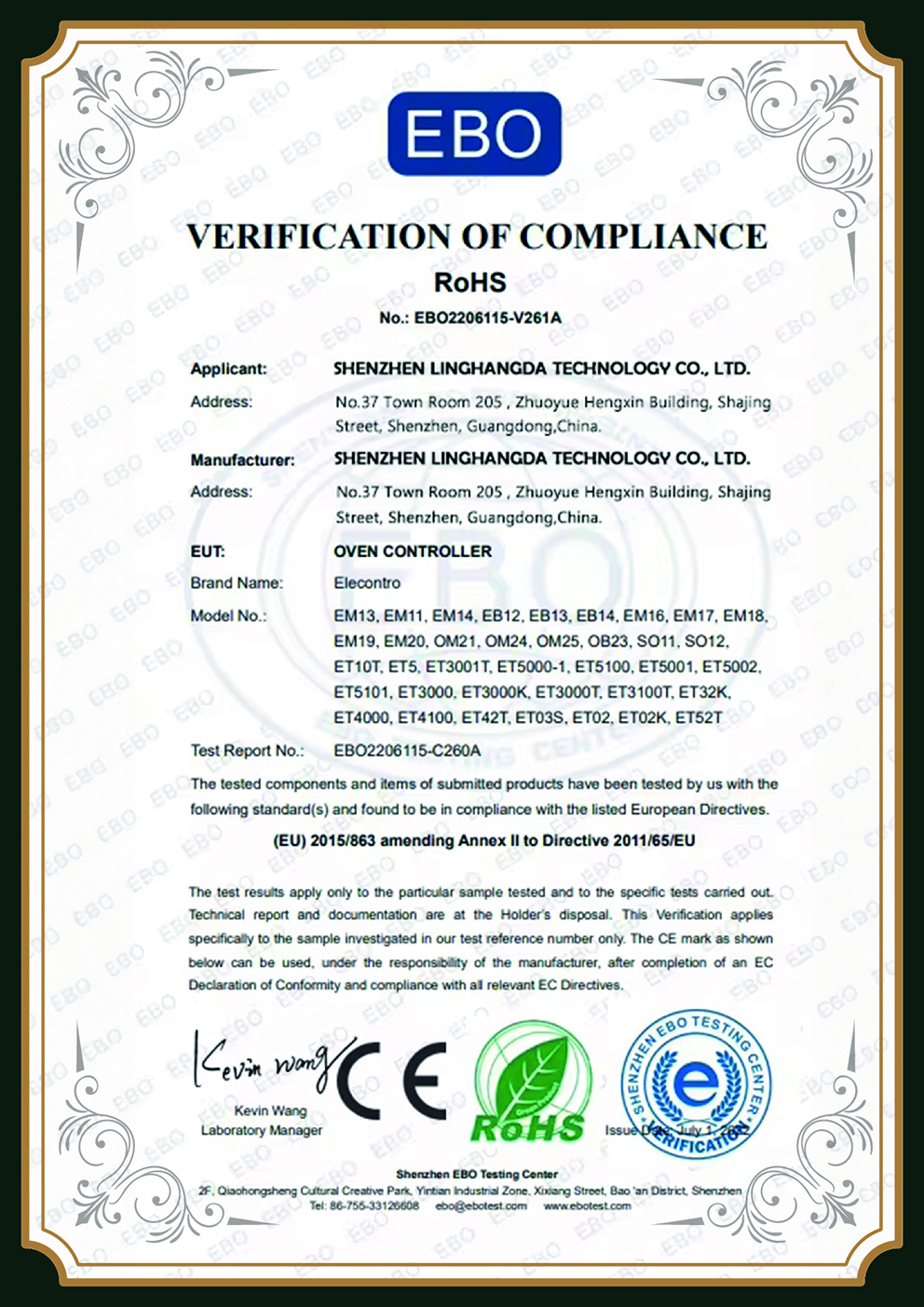
Quality system
Our quality system is ISO 9001-based and audited under IATF 16949, the stricter automotive scheme that embeds ISO 9001 conformance. For material compliance, we build RoHS-compliant boards and offer halogen-free laminates, verified in-house with an X-ray fluorescence RoHS/halogen analyzer — a manufacturing capability, distinct from any finished-product mark.
Supplier transparency
- Huizhou Linghangda Technology Co., Ltd. PCB fabrication
- Shenzhen Linghangda Technology Co., Ltd. PCB assembly
"PCBark" is the trade name of these legal entities. The IATF 16949, ISO 14001, and UL records are held under them; certificate numbers are provided on request for audit verification.
Request certificate numbers for audit verificationOrdering 8–12 Layer PCBs: Files, Lead Time and Total Cost
Unit price is only the tip of the iceberg. Independent procurement analyses put the hidden cost of a poorly vetted supplier at 20–40% above the quoted price once rework, scrap, and delays are counted, and a board that fails in the field costs 10–20× more to fix than one caught in production. That math is why 100% electrical test is a cost lever, not an expense.
10–20×
Industry estimates put the cost of fixing a defective board in the field at 10–20× the cost of catching it during production.
Source: industry TCO analyses (illustrative market average, not PCBark-specific data)What you send, and what you get back
- Files send Gerber (RS-274X) or ODB++, plus a stackup drawing and impedance targets for controlled-impedance work.
- MOQ none; we run quick-turn prototypes through to volume on the same lines.
- Lead Time Lead time scales with layer count and area, and each added pair of layers adds roughly 3–5 days of process time.
- DFM a free design-for-manufacturing review comes with every quote, with stackup and impedance feedback before tooling.
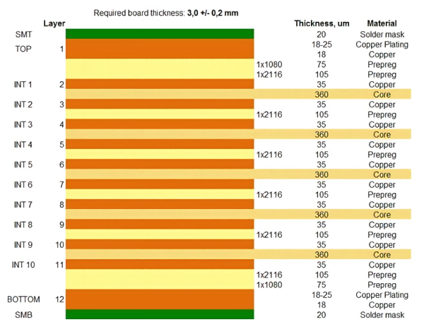
That trade-off is predictable: published cost models show roughly a 20–30% rise moving from 8 to 10 layers, and again from 10 to 12, so 12 layer pcb cost climbs with every plane pair you add. We use that data to help you right-size the layer count rather than over-build it.
Cadence layer-count cost analysis8–12 Layer PCB Design Tools
-
Selector
Layer Count Selector
Choose the right layer count for an 8–12 layer board based on routing density and signal needs.
Open tool -
Estimator
PCB Cost Factor Estimator
Break down the variables that drive multilayer PCB pricing to estimate cost factors before you quote.
Open tool -
Calculator
Impedance Trace Calculator
Calculate controlled-impedance trace width and spacing from your stackup parameters.
Open tool -
Selector
IPC Class Selector
Determine which IPC class applies to your board's reliability and acceptance requirements.
Open tool
01
What is the standard thickness of a 12-layer PCB?
1.6 mm is the standard baseline, and we build 12-layer boards there with standard processes. In practice most 8–12 layer designs finish between 1.6 mm and 3.2 mm once copper weight and impedance control are set.
02
Are 12-layer PCBs always HDI, and is FR-4 enough?
No on both counts. Many 8–12 layer boards use through-hole and standard FR-4 or High-Tg material. HDI microvias and low-Dk materials like Rogers only come in when fine-pitch BGAs or signals above ~1 GHz demand them.
03
How do you guarantee impedance and signal integrity?
We design the stackup to your 50 Ω single-ended and 100 Ω differential targets, hold tolerance to ±5–10%, and confirm it with time-domain reflectometry on a coupon before the lot ships. Dedicated ground and power planes sit next to every signal layer to keep return paths short, and on high-speed nets we back-drill the via stubs and apply the 3-W spacing rule so crosstalk stays controlled.
04
What via types do you offer on 8–12 layer boards?
Through-hole, blind, buried, and laser microvias, with resin-plugged or copper-filled options and via-in-pad for fine-pitch BGAs. Stacked microvias are available on advanced HDI builds.
05
Why does 100% electrical test matter more than AOI on multilayer boards?
Automated optical inspection only sees outer surfaces; it cannot confirm that buried vias connect to internal layers. Only an electrical test catches an open inner net — which is why every panel gets one.
06
What quality standards and certifications do you hold?
IATF 16949:2016 and ISO 14001:2015 (both current and certification-body verifiable), UL recognition for multilayer printed wiring boards (File E316475), and build/inspection to IPC-A-600 and IPC-6012 Class 2 and Class 3.
07
Is there a minimum order quantity?
No. Prototype and production run on the same lines, so you scale without switching fabs.
08
How do I choose between 8, 10 and 12 layers?
Honest answer — start from your fastest signal, your plane count, and your densest BGA pitch, not a target layer number. Send us the net list and we will recommend the lowest layer count that meets your signal-integrity and reliability goals — more layers is not always the right call.