Get in touch with PCBark Company



Updated July 2026 · Reviewed by the PCBark technical team.
A multilayer flex PCB is a flexible printed circuit with three or more copper layers bonded into a single bendable stack. Designing one means fighting a trade-off on every layer: the copper you add to route more signals also stiffens the board and shrinks the bend radius it can survive. A four-layer flex circuit isn’t simply a two-layer board with more routing, it moves the copper away from the neutral bending axis, raises internal strain, and changes which failure modes you’ve to design against. This guide covers the stackup, materials, bend-radius math, via architecture, and IPC-6013 reliability rules that separate a flexible printed circuit that lasts from one that delaminates. Those design guidelines apply whether you’re stacking multiple layers of copper onto a single flexible substrate or weighing that build against a simpler single-layer flex.
A multilayer flex PCB is a flexible printed circuit built from three or more copper conductive layers, joined by plated through-holes and separated by polyimide dielectrics (IPC-6013 Type 3). It’s engineered for static, bend-to-install, high-density interconnect applications, not for repeated dynamic flexing, which single- or double-layer flex handles far more reliably.
Key Takeaways
- More layers does not mean more flexible. Each added conductive layer pushes copper off the neutral axis, so multilayer flex is mainly a static/bend-to-install technology, dynamic hinges use single- or double-layer flex, with unbonded “bookbinder” construction the one specialist exception.
- There’s no single authoritative bend-radius multiplier, published rules of thumb disagree (multilayer static quoted anywhere from 10x to 24x thickness). The defensible method is the outer-fiber strain model, not a table lookup.
- Rolled-annealed (RA) copper delays fatigue-crack initiation markedly longer than electrodeposited (ED) copper, a settled metallurgical result driven by grain structure, with published multiples varying by test.
- Flex acceptance is governed by the current IPC-6013E (performance, Sept 2021) and IPC-2223F (design, 2026) — not the older revisions many vendor guides still quote.
Quick Specs, Multilayer Flex PCB
| IPC-6013 classification | Type 3 (multilayer flex, 3+ conductive layers with PTH) |
| Typical layer count | 3–8 layers (10–12 achievable via bookbinding) |
| Base film | Polyimide, 12.5–50 µm per layer |
| Conductor | Rolled-annealed copper, 12–35 µm (0.5 oz for dynamic) |
| Coverlay | Polyimide + adhesive, 25–50 µm |
| PTH plating (Type 3/4) | 25 µm average copper |
| Primary use | Static / bend-to-install, high-density interconnect |
What Is a Multilayer Flex PCB, and When Should You Use One?

A multilayer flex PCB is a flexible circuit board with three or more copper conductive layers laminated onto polyimide dielectrics and connected by plated through-holes, classified as IPC-6013 Type 3. It replaces bulky point-to-point wiring or a rigid board where you need high-density interconnect in a shape that folds to fit a housing.
Among flexible circuit technologies, it sits above single-sided flex and double-sided flex, one or two copper layers give you a bendable cable, while a multilayer flexible stack gives you real routing density in a compact design. That design freedom, a genuinely miniaturized design in a small volume, is the whole reason to accept the extra process complexity. The counterintuitive part is that it isn’t built for constant motion, it’s built to be formed once and stay put.
That distinction matter because the most common assumption about these boards is wrong. Field guidance is blunt about it: “the dynamic bending stress can only be reliably ensured with single- and double-layer flexible circuits.” The one exception is specialist unbonded or “bookbinder” construction, where the flexible layers slip relative to one another instead of bending as a bonded stack, IPC-2223F covers it, but it’s the edge case, not the default. A multilayer flex PCB earns its place when routing density, controlled impedance, or shielding forces you past two layers and the assembly only has to bend into position during installation, a camera module folding into a phone, a stacked sensor board wrapping a cylindrical housing, an avionics interconnect that packs into a tight bay. These applications of flexible PCBs, from flex cables inside a laptop hinge to stacked sensor boards wrapped around a housing, all trade repeated motion for density.
💡 Pro Tip
If your product hinge flexes tens of thousands of times over its life, do not reach for a multilayer stack. Split the design: keep the dynamic hinge as a single- or double-layer flex tail and concentrate the layers where the board is static.
Flex Materials: Polyimide, RA-vs-ED Copper, and Coverlay
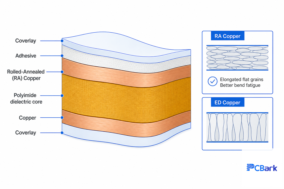
Copper type is the single biggest reliability decision in flexible PCBs, and most guides skip it. Copper foil comes in two forms: electrodeposited (ED), whose columnar grain structure is brittle under repeated bending, and rolled-annealed (RA), whose elongated grain structure resists fatigue. That grain difference gives RA a decisively longer bend-fatigue life than ED; the exact multiple vary by test setup, but the direction is well established across the fatigue literature which is why RA copper is effectively mandatory in any bend zone.
Next comes the laminate system, the dielectric substrate that defines the structure of flexible circuits. Adhesive-based construction uses an acrylic bond layer with a very high Z-axis coefficient of thermal expansion, which drives plated through-hole barrel cracking during reflow. Adhesiveless (cast) polyimide such as the laminates used in flexible printed circuits removes that interface entirely, so it survives reflow and thermal cycling far better than an adhesive build, the settled, physics-based reason to specify it whenever a bend zone will see heat. One low-profile 2024 study reports a meaningful flex-life improvement from going adhesiveless; treat that as a directional finding to confirm against your material supplier’s datasheet, not a settled figure.
| Material choice | Option A | Option B (bend-zone default) | Why it matters |
|---|---|---|---|
| Copper foil | ED (columnar grain) | RA (elongated grain) | RA delays crack initiation far longer |
| Laminate | Acrylic-adhesive | Adhesiveless / cast polyimide | Longer flex life; lower Z-CTE |
| Copper weight (bend) | 1 oz (35 µm) | 0.5 oz (12–18 µm) | Thinner copper = lower bend strain |
| Surface protection | Liquid solder mask | Coverlay (polyimide + adhesive) | Coverlay flexes; solder mask cracks |
Coverlay is worth calling out on its own. Unlike the liquid solder mask on a rigid board, coverlay is a solid polyimide film with an adhesive layer, die-cut or shaped by laser cutting to expose pads. Keep the coverlay dam at a minimum of 10 mils, and remember coverlay can’t register over very tight-pitch components, those need photoimageable coverlay or a stiffener instead.
Symmetric Stackup and the Neutral-Axis Stackup Rule
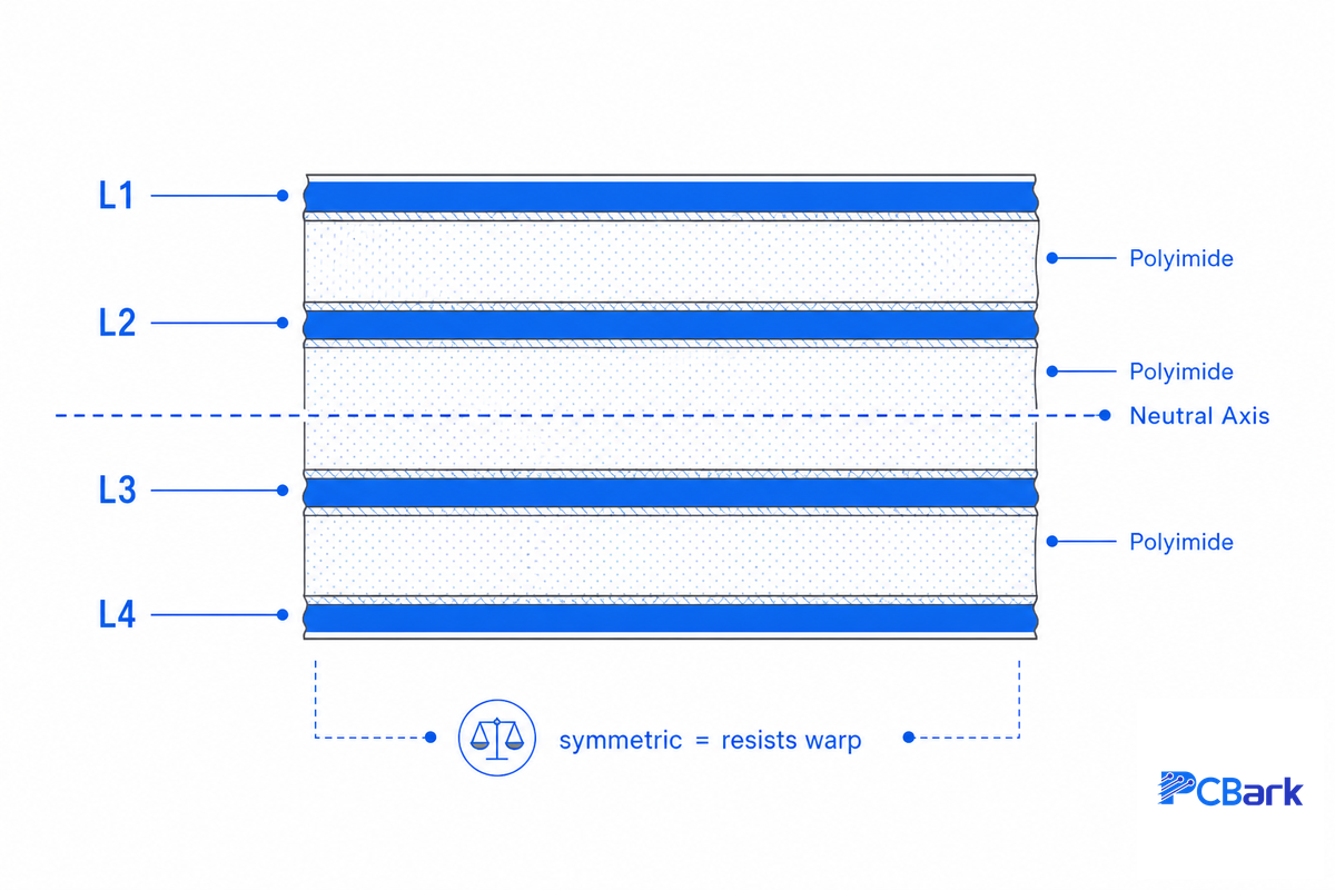
Every flex PCB stackup answers to one principle. The Neutral-Axis Stackup Rule: in a bend, the mechanical strain is zero at the center of the stack and maximum at the outer surface, so the goal is to keep the most fatigue-sensitive copper as close to that neutral axis as the layer count allow. Every layer you add moves the outer conductors farther from the center and raises their strain, the mechanical penalty of density.
Two construction rules follow. First, avoid the I-beam effect: never place copper traces on opposing layers directly on top of one another, because stacked copper forms a stiff beam that concentrates stress. Stagger the traces between layers instead. Second, replace solid copper planes in the bend zone with a cross-hatched pattern, a common parameter set is 15 mil (0.38 mm) trace width on 25 mil (0.63 mm) spacing, so the plane can flex. On this point, industry authority is explicit:
“For maximum dynamic flex life and reliability, conductors in the bend area should be routed perpendicular to, and evenly spaced across the bend area… The neutral bend axis, where possible, should be located at the center of the conductor pattern… when two metal flexible circuits are required, the circuit path on each side must be offset from one another to prevent stress in the copper foil.”
Vern Solberg, independent technical consultant, “Designer’s Notebook,” I-Connect007
How Many Layers? The Via-Integrity Ceiling
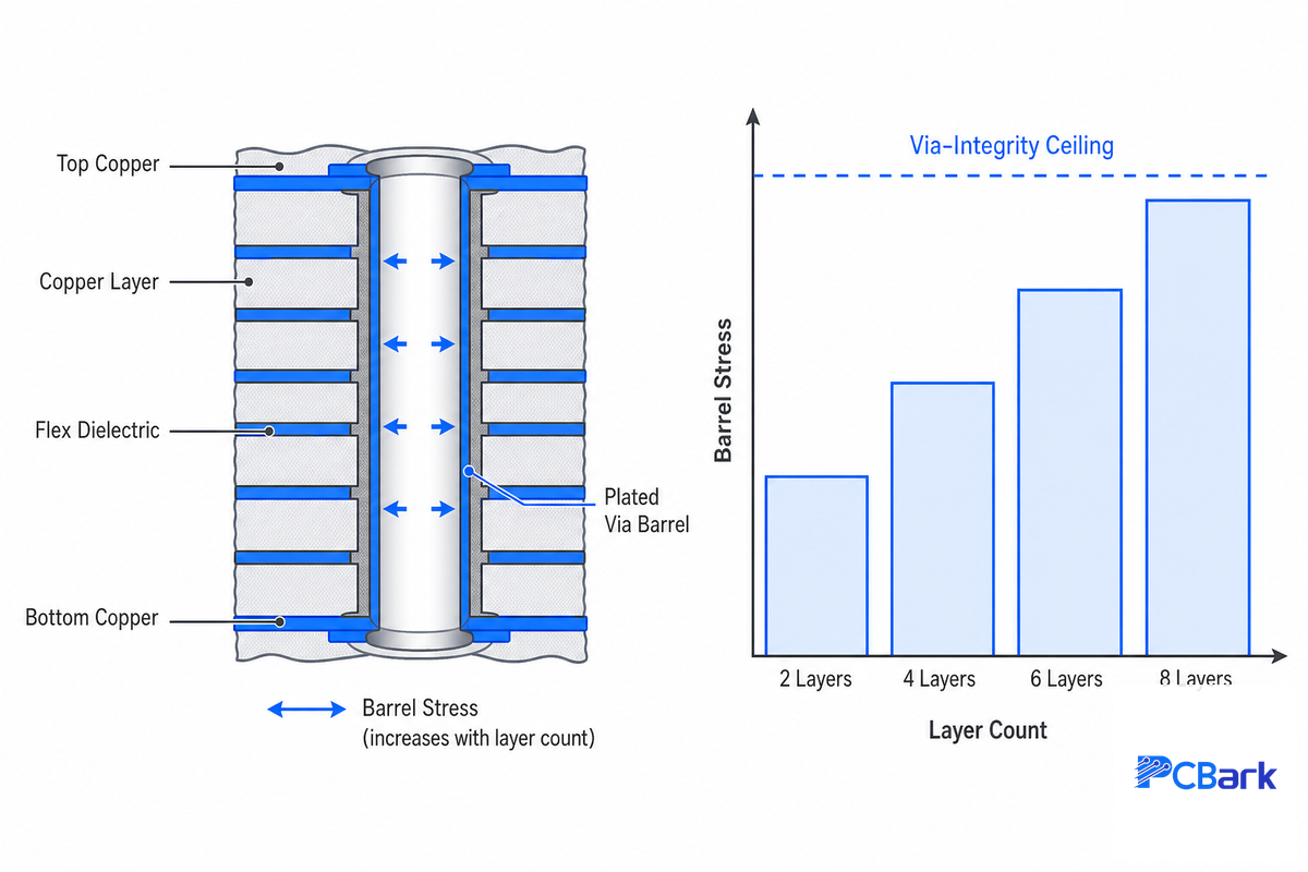
The right layer count is the lowest one that satisfies your net count, impedance references, and shielding, because every layer beyond that raises the total thickness and lowers the bend reliability. We call this the Via-Integrity Ceiling: the practical layer count above which added routing density starts costing you more via and bend-fatigue margin than it buys.
Here’s the mechanism. Thicker stacks force a larger minimum bend radius; at the same time, plated through-holes concentrate stress. In flex-fatigue testing, dynamically flexed multilayer vias fail rapidly once the radius drop below roughly 10x the circuit thickness. So the question isn’t “how many layers can I fab?” but “how many layers can this bend geometry keep reliable?” Field teams see this the hard way, a six-layer wearable prototype that misses its yield and bend targets, redesigned to four layers, hits every spec. Multilayer flex circuits earn their layers only when density truly demands it; where a single-layer design, or plain single-sided or double-sided circuits, can carry the signals, they’ll outlast a thick stack in any dynamic bend. Use a structured layer-count decision for your multilayer flex build rather than defaulting to the highest count your router will accept.
| Layers | IPC-6013 type | Dynamic flex? | Best fit |
|---|---|---|---|
| 1 (single-sided) | Type 1 | Yes — best | Dynamic hinges, moving heads |
| 2 (double-sided) | Type 2 | Yes — good | Repeated flex + some density |
| 3–4 | Type 3 | Static / limited | High-density, one-time form |
| 6 | Type 3 | Static only | Impedance + shielding |
| 8 | Type 3 | Static only | Dense backplanes, bend-to-install |
| 10–12 | Type 3 (bookbinding) | Rare / specialist | Loose-leaf, unbonded flex bundles |
Controlled Impedance on Flex
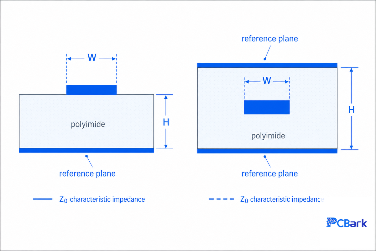
Controlled impedance behaves differently on flex than on rigid FR4, and two effects catch designers out. First, polyimide has a lower dielectric constant, roughly Dk 3.2–3.5 versus about 4.3 for FR4, and the dielectrics are thin (25–50 µm), so hitting 50 Ω forces very narrow traces. Second, the cross-hatched reference plane you need for flexibility isn’t solid copper: it no longer provides 100% shielding, so the controlled impedance of the signal traces rise versus a solid plane and must be modeled that way. On high-speed differential links, a hatched reference also introduces position-dependent impedance and return-path asymmetry, so treat it as a field-solver problem rather than a single correction factor. A general transmission-line rule still holds, every signal and power trace needs a continuous adjacent return plane but on flex you tune the trace geometry around a hatched reference, not a solid one.
Because a bonded reference plane also stiffens the flex, controlled-impedance multilayer flex is almost always a static application. If your impedance requirements are tight and you also need a rigid mounting region, that’s a signal you may want a denser HDI approach compared against a standard multilayer build rather than more flex layers.
Minimum Bend Radius Worksheet
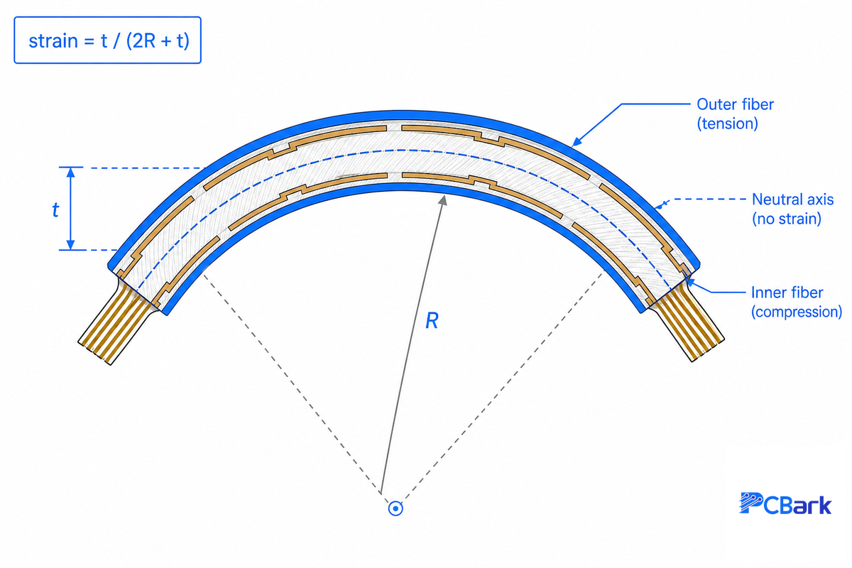
Skip the multiplier tables, they disagree with each other. Published rules of thumb put the multilayer static minimum bend radius anywhere from 10x to 24x total thickness, all citing IPC-2223, and dynamic figures range from 100x to 150x. They conflict because a multiplier hides the real variable, which is outer-fiber strain. The defensible calculation is:
📐 Engineering Note — the strain equation
Strain (%) = [ t / (2R + t) ] × 100, where t = total flex thickness and R = inside bend radius. Solved for the minimum radius at an allowable strain ε (as a fraction): Rmin = t (1 − ε) / (2ε). Design limits: keep RA-copper dynamic strain under ~0.3%, and static strain under ~10%.
Worked example. Take a four-layer flex with a total flex PCB thickness of 0.30 mm. For a static, bend-to-install fold at a 10% strain limit, Rmin = 0.30 × (1 − 0.10) / (2 × 0.10) = 1.35 mm. For the same board flexed dynamically at a 0.3% strain limit, Rmin = 0.30 × (1 − 0.003) / (2 × 0.003) ≈ 50 mm. That 37x jump, from a 1.35 mm fold to a 50 mm hinge, is the quantitative reason multilayer flex is a static technology: nobody packages a 50 mm bend radius into a handheld. Run your own numbers with a multilayer flex bend radius calculation before you commit a stackup.
💡 Pro Tip
A practitioner rule of thumb from EEVblog — “keep the bend radius to at least 10 times the thickness of the material,” so 0.5 mm polyimide wants a 5 mm radius minimum — is a fine sanity check for single/double-layer flex, but always fall back to the strain equation for multilayer stacks.
Vias, Coverlay, and Stiffeners
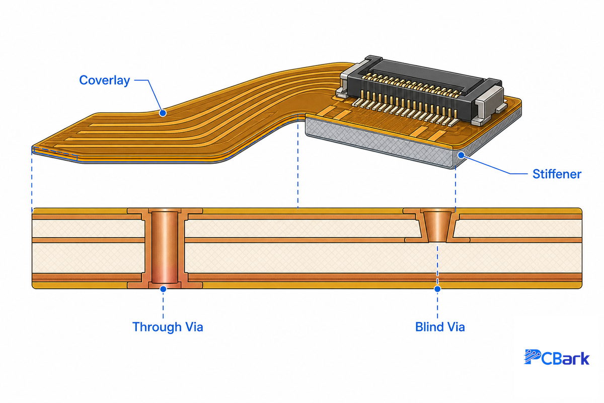
Vias are where multilayer flex reliability is won or lost, because a plated barrel is rigid and the dielectric around it isn’t. Barrel cracking traces to a coefficient-of-thermal-expansion mismatch: heating a laminate with a large CTE difference generates shear at the bonding interface. NASA’s Goddard workmanship research documents this mechanism generally, an interfacial shear driven by a roughly 10x CTE difference in rigid glass/epoxy builds and in flex it’s the acrylic adhesive’s high Z-axis CTE that plays the same villain during reflow.
Design rules follow directly: place vias at least 20 mils from any rigid-to-flex interface, keep them out of active bend zones entirely, teardrop them, and add up to 1.5 mils of extra through-hole plating for mechanical support. IPC-6013E tightened this area, paragraph 3.4.2 now explicitly requires a 0.001 in minimum annular ring where no pad fillets are present, and Type 3/4 builds carry a 25 µm average PTH copper minimum. Keep via-to-bend clearance at 1.0 mm for static designs and 1.5 mm for dynamic, and hold components and stiffeners at least 2.5 mm off the bend. Stiffeners, polyimide for ZIF connector tabs, FR4 or stainless for structural support, go under component and connector areas, never across a bend. A design-for-manufacturing review of the flex stackup should confirm every via sit outside the bend and transition zones before release.
Failure Modes and IPC-6013 Reliability
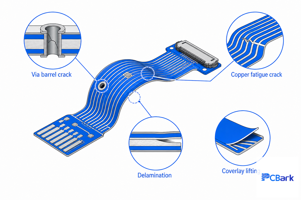
Most multilayer flex failures are latent: the board passes a flat electrical test, then fails after folding or reflow. That’s why IPC-6013E qualification leans on mechanical and thermal stress testing, flexural endurance per IPC-TM-650 Method 2.4.3, thermal cycling, and thermal-shock coupons, rather than a bare continuity check. This table maps the failure modes you actually design against to their root cause and mitigation.
| Failure mode | Root cause | Mitigation |
|---|---|---|
| Conductor fatigue cracking | ED copper grain / bend strain | RA copper, 0.5 oz, larger radius |
| Via barrel cracking | Acrylic adhesive Z-CTE shear at reflow | Adhesiveless laminate, teardrops, keep-out |
| Delamination / blistering | Polyimide moisture (1–3%), skipped pre-bake | Pre-bake, moisture-barrier handling |
| Coverlay-edge foil crack | I-beam stress from stacked traces | Stagger traces, offset opposing layers |
| Pad lift | Flex at pad edge, thin anchor | Anchor pads, stiffener under pads |
| CAF (conductive filament) | Moisture + bias across dielectric | Adhesiveless build, spacing, seal |
| Transition-zone foil crack | Abrupt rigid-to-flex step | Teardrop, ≥20 mil via keep-out |
| Impedance drift | Hatched plane / dielectric variation | Model hatched reference, control thickness |
| Warp / twist | Asymmetric copper, unbalanced stack | Symmetric stackup, copper balancing |
Two evidence points anchor the moisture and fatigue rows. Adding a polyimide substrate in one thin-copper fatigue study raised cycles-to-failure from hundreds into the thousands, confirming the base film’s role, while the via-fatigue threshold below 10x thickness shows how quickly reliability collapses when the bend radius is too tight. Flex acceptance itself is governed by the current IPC-6013E (September 2021, replacing the amended Revision D) alongside the design standard IPC-2223F.
Multilayer Flex vs Rigid-Flex
Of the common types of PCBs, multilayer flex (IPC-6013 Type 3) is an all-flexible stack, while rigid-flex (Type 4) laminates rigid layers into the flexible ones. Where a plain rigid circuit, or a pair of separate rigid PCBs, would force a cable-and-connector break between boards, bonding a rigid PCB region directly to the flex folds that interconnect in. The practical difference is mechanical support: a fully flexible multilayer board has no rigid region to mount connectors or heavy components, so where you need both a stable mounting island and a folding interconnect, rigid-flex is the answer, a flex circuit can’t always replace it. Rigid-flex also costs more to build; its layered fabrication process is complex enough to be the subject of dedicated construction patents.
| Attribute | Multilayer flex (Type 3) | Rigid-flex (Type 4) |
|---|---|---|
| Construction | All flexible layers | Rigid + flexible sections |
| Component support | Needs stiffeners | Rigid islands built in |
| Relative cost | Lower | Higher |
| Best for | Fold-to-fit dense interconnect | Board-to-board with mounting |
If your bill of materials includes connectors, shielding cans, or fine-pitch parts that need a flat rigid landing, compare a rigid-flex PCB and a rigid multilayer PCB with a separate flex jumper before defaulting to an all-flex Type 3 stack.
DFM and Cost: The Static-vs-Dynamic Decision Matrix

Two upstream decisions set most of your cost and yield: whether the board is static or dynamic, and which IPC performance class it targets. Flexible dielectric is dimensionally unstable, it moves and shrinks during processing, so drill-to-copper should stay at a minimum of 8 mils, and registration on thin films drives yield. On class, an IPC-6013 Class 3 build carries a cost premium over Class 1/2, but no fixed percentage is published: the premium come from stricter inspection (no annular-ring reduction, mandatory cross-section coupons), lower yield, and added thermal-cycle and vibration testing. Even small geometry choices move the number, one practitioner notes that lengthening a flex tail is expensive: “2mm is a very high cost.”
| Design parameter | Static (bend-to-install) | Dynamic (repeated flex) |
|---|---|---|
| Layer count | 3–8 (multilayer OK) | 1–2 only |
| Allowable strain | Up to ~10% | < ~0.3% |
| Bend radius (0.30 mm) | ~1.35 mm | ~50 mm |
| Copper | RA preferred | RA mandatory, 0.5 oz |
| Laminate | Adhesive acceptable | Adhesiveless |
| Vias in bend zone | Avoid | Never |
| Bend-zone copper | Cross-hatched plane | Cross-hatched, staggered |
| Qualification | Install-flex + thermal | IPC-TM-650 2.4.3 cycling |
| Cost driver | Layer count, coverlay | Material grade, test cycles |
Industry Outlook: Design Knowledge Is Moving In-House

For a flex PCB designer, the most useful trend isn’t the market size, it’s who’s now making the design decisions. Search-demand signals show engineers and buyers pulling flex design and material knowledge in-house: queries for polyimide and multilayer PCB design are climbing year over year, while navigational “flex PCB manufacturer” searches are falling. Read practically, the design of flexible circuits, RA copper, adhesiveless laminate, a neutral-axis-aware layer count, is becoming the buyer’s job, not something to leave at the supplier’s default. Design challenges that once sat with the fabricator now belong to whoever owns the schematic, which is why design practices and design options that used to be tribal knowledge are being written down.
That shift is reinforced by the standards themselves. IPC-6013E (2021) and IPC-2223F updated bend-area and annular-ring guidance, and adhesiveless materials plus bookbinding constructions keep pushing what a Type 3 stack can survive. Against that backdrop, the market context is a tailwind rather than the story: independent forecasts put the flexible PCB market on a roughly 12–14% CAGR through the early 2030s, order-of-magnitude directional numbers that say demand is healthy without telling you anything about your stackup. If you’re planning a 2026 program, the actionable move is to write RA copper, adhesiveless laminate, and a neutral-axis stackup into your specification now, rather than discovering them at first-article failure.
Frequently Asked Questions
Q: How many layers can a multilayer flex PCB have?
View Answer
A multilayer flex PCB (IPC-6013 Type 3), unlike a basic single-layer flex circuit board, has three or more conductive layers, with 3 to 8 layers typical for high-density static designs. Counts of 10 to 12 layers are achievable using bookbinding or loose-leaf construction, but each added layer raises total thickness, forces a larger bend radius, and lowers dynamic reliability — so the practical ceiling is set by your bend geometry, not the fabricator.
Q: What is the minimum bend radius for a multilayer flex PCB?
View Answer
There is no single multiplier — published rules of thumb range from 10x to 24x thickness for static bends and up to 150x for dynamic, which is why the strain equation is more reliable. Using Strain (%) = t / (2R + t) × 100, a 0.30 mm four-layer board needs about a 1.35 mm radius for a static fold (10% strain) but roughly 50 mm for repeated dynamic flexing (0.3% strain). That gap is why multilayer flex is used for static, bend-to-install designs.
Q: Why use rolled-annealed copper instead of electrodeposited copper?
View Answer
Rolled-annealed (RA) copper has an elongated grain structure that resists bending fatigue, while electrodeposited (ED) copper has a columnar grain structure that cracks under repeated flex. Independent fatigue testing consistently shows RA copper delaying fatigue-crack initiation substantially longer than ED under identical conditions, which makes RA effectively mandatory in any flex bend zone, especially for dynamic applications.
Q: Is multilayer flex the same as rigid-flex?
View Answer
No. A multilayer flex PCB (Type 3) is fully flexible; a rigid-flex PCB (Type 4) combines rigid and flexible sections in one board, giving you rigid mounting islands for connectors and heavy parts. Both are distinct branches of flexible PCB design, chosen by whether the assembly needs a rigid landing area.
Q: What standard governs multilayer flex PCB acceptance?
View Answer
IPC-6013E (Rev E, September 2021) covers performance and qualification, and IPC-2223F covers flex design. Rev D is superseded.
Q: Can you put vias in the bend area of a flex circuit?
View Answer
No — keep plated through-holes out of active bend zones and at least 20 mils from any rigid-to-flex transition. Vias flexed in a bend crack quickly; teardrop them and add up to 1.5 mils of plating for support.
Get a flex or rigid-flex DFM review before you fabricate
Get a DFM review of your stackup, bend zones, and via placement before you release. PCBark builds multilayer flex, rigid-flex, and HDI boards under IPC-6013 with turnkey assembly.
About This Engineering Guide
This multilayer flex PCB design guide compiles bend-radius strain math, RA-vs-ED copper fatigue data, and IPC-6013E via and reliability rules from standards bodies, NASA workmanship research, and named flex-design authorities, not vendor marketing. Where sources disagree, such as the conflicting bend-radius multipliers, we show the disagreement and give you the underlying calculation instead, the kind of PCB design detail that separates a reliable flexible PCB from a field return. Reviewed by the PCBark technical team.
References & Sources
- Printed Circuit Board Reliability, CTE and Via Barrel CrackingNASA Goddard Space Flight Center (B. Sood)
- Flexible PCB Fatigue and Polyimide Substrate Cycles-to-Failure StudyU.S. National Institutes of Health (PMC)
- Material and Reliability Guidelines for Flexible PCBs in Class 3 (2024)Int’l Journal of Advanced Engineering Technology and Innovation
- Characterization of Rolled-Annealed Copper Film Fatigue in FPCsMicroelectronics Reliability (Elsevier)
- What’s New in IPC-6013ENick Koop (IPC-6013 subcommittee co-chair), PCD&F
- Designer’s Notebook: Flexible and Rigid-Flex Circuit Design PrinciplesVern Solberg, I-Connect007
- Design PCBs for EMI, Basic Stack-UpKenneth Wyatt, EDN
- US5144742A, Method of Making Rigid-Flex Printed Circuit BoardsGoogle Patents
- Flexible Printed Circuit Boards Market ReportGrand View Research (market context)
Related Articles
- Aerospace PCB Design GuideClass 3 flex and rigid-flex for avionics
- Medical PCB Design Guideflex circuits for wearables and implantables
- PCB Assembly Guidehandling and reflow for flex boards