Get in touch with PCBark Company

High Density Interconnect PCB Manufacturing
HDI PCB Manufacturing — High-Density Interconnect Boards from Prototype to Volume
Once you pass about a 0.5 mm BGA pitch and start stacking more layers on top of layers, a traditional multilayer PCB can’t even be the solution. PCBark has been designing HDI PCBs, utilizing laser microvias, blind/buried vias, via-in-pad, and any-layer fabrication to create PCBs so your routes go further with fewer traces in fewer layers while maintaining the signal integrity you expect. And one partner manages it all—DFM, build, sourcing, and assembly.
Specifications
Layer Count
4–40+
Layer count, rigid & rigid-flex HDI
Min Laser Microvia
3 mil
Min laser microvia (0.075 mm)
Min Line / Space
2 mil
Min line / space (50 µm)
Build Structures
Any-Layer
1+N+1 · 2+N+2 · 3+N+3 · ELIC
Reliability Class
IPC-6012
Class 2 & Class 3 build options
Service Model
Turnkey
DFM → fab → sourcing → assembly
01 / The Problem
When Standard Multilayer PCBs Run Out of Space — HDI Solves It
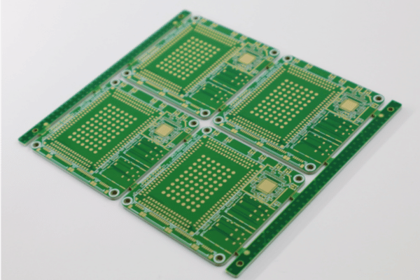
Your components now define the board, not the reverse. Whether it’s a 0.4 mm pitch BGA, a module-in-a-chip, or even a stack of high-speed radio components, the pads on these modern components cannot be serviced with standard plated through-hole vias. The usual solution? Throwing another layer at it. But doing so drives layer counts and board thickness sky-high without decreasing signal length. HDI PCBs attack the problem differently—by using laser-drilled microvias and stacked copper structures to pack much more wiring capacity into the surface of your PCB. This makes room for significantly more traces to fit into fewer layers.
Throwing another layer at it — driving layer count and board thickness sky-high without decreasing signal length.
Laser-drilled microvias and stacked copper structures pack more wiring into the surface — more traces in fewer layers.
02 / The Standard
Built to the HDI Design Standard — IPC-2226
HDI PCBs are a design standard (IPC-2226) for precisely that. Rather than relying on only a single style of plated through-hole, HDI boards mix several—microvias, blind vias, buried vias, and via-in-pad, all combined with very fine line width down to 2 mils. This yields an HDI printed circuit board that allows for tighter component spacing and reduced wire lengths, which enables high-speed signal integrity required in devices from smartphones and wearable computers to avionic equipment.
- Microvias
- Blind vias
- Buried vias
- Via-in-pad
- Line width down to 2 mils
01 / Capabilities
PCBark HDI PCB Capabilities — Stack-Ups, Vias & Specs
Buyer Focus: Engineering (Primary), Procurement (RFQ Match) Our HDI lines cover every stack-up type: a single layer of microvias over a multilayer base to multiple layers of microvias—including any-layer constructions. Refer to the table below to know where our manufacturing team operates. Any stack-up that fits neatly within the stated parameters and tolerance should be quotable; any stack-up that pushes the boundaries will trigger a notification in DFM before the job goes to production.
| Capability | Standard | Advanced |
|---|---|---|
| Layer count | 4 – 20 layers | up to 40+ layers |
| HDI structure | 1+N+1, 2+N+2 | 3+N+3, Any-Layer (ELIC) |
| Laser microvia diameter | 0.10 mm (4 mil) | 0.075 mm (3 mil) |
| Microvia aspect ratio | 0.8 : 1 | 1 : 1 |
| Min line / space | 3 mil / 3 mil (75 µm) | 2 mil / 2 mil (50 µm) |
| Mechanical drill (PTH) | 0.20 mm | 0.15 mm |
| Board thickness | 0.4 – 3.2 mm | 0.2 – 4.0 mm |
| Via fill | Resin / copper-filled | Stacked & staggered, capped via-in-pad |
| Materials | FR-4, High-Tg | Rogers, polyimide, mixed dielectric |
Note that industry standard HDI fabrication capabilities adhere to IPC-2226; specifics will depend on the exact stack-up and can only be finalized once designs are brought in for DFM analysis. See “References” for detailed specifications.
02 / Design & Vias
The Microvia Is the Controlling Variable
Good HDI PCB design starts in PCB layout, not on the production floor. Earlier commitment from your PCB designers — to a microvia strategy, a PCB stack-up, and an intended number of layers — keeps the handoff from design and manufacturing into our production process clean. Our process treats the microvia as the controlling variable in HDI technology — everything else on these HDI circuit boards, from outer layer line width to material, flows from it, and the via-technology limits we hold are what let a high-density PCB yield instead of fighting you. That is the real advantage of HDI manufacturing: fewer layers, tighter routing, and HDI printed circuit boards an assembler can build the first time.
Via types we build
Microvias: The heart of any HDI design – laser-drilled holes, typically 0.10 mm and smaller, connecting adjacent layers. We stack and stagger them through sequential lamination, build buried vias within the core and form blind vias from the outside in. On fine-pitch components, we place via-in-pad – a copper-filled and planarized microvia, set within the SMD pad itself, plated flat for optimal solder paste printing. Each structure in that sequence involves a distinct plating and laminate step, which explains why HDI design rules and aspect ratios so crucially impact final yields.
Microvia Aspect Ratio
The aspect ratio is determined by dividing via depth by its diameter, and on laser microvias, it determines if the plated through-hole can consistently carry the load. Stacked microvias with aspect ratios around 0.8:1 ensure uniform copper coverage, whereas longer dielectric spacing will result in plating thinning down into the hole. Typically, our aspect ratio for microvias involves a 3 mil dielectric and 3-4 mil laser vias. This aspect ratio keeps microvias within reliable limits. It’s one of the first parameters checked on an arriving design package.
03 / Choose Your Stack-Up
Choosing Your HDI Stack-Up
In most cases, HDI isn’t about pursuing extreme design—it’s about selecting the right one. Use this decision tree to match the HDI designs outlined here to the right kind of PCB and estimate the cost impact of a more densely populated design.
| HDI structure | Build-up layers | Best-fit application | Relative cost |
|---|---|---|---|
| 1+N+1 | 1 microvia layer / side | Single fine-pitch BGA, IoT & wearable | $ |
| 2+N+2 | 2 microvia layers / side | Smartphone, dense consumer, automotive ECU | $$ |
| 3+N+3 | 3 microvia layers / side | High-pin-count SoC, networking | $$$ |
| Any-Layer (ELIC) | All layers stacked microvia | Flagship mobile, AI module, aerospace | $$$$ |
04 / Explore Further
Related HDI Topics
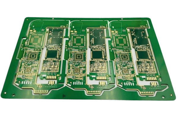
Any-Layer HDI PCB
Understanding HDI: Microvias – The Key. Image: Using ELIC any-layer design to place ELIC any-layer structures on your circuit boards – stack copper-filled microvias on every layer and make any layer connect to any other layer on your dense PCB.
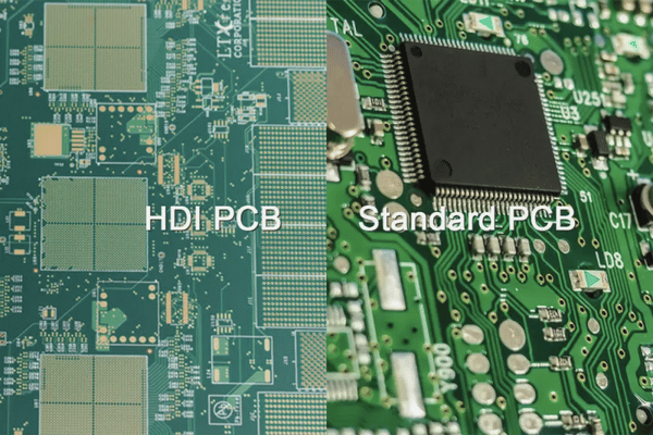
HDI vs Standard Multilayer PCB
HDL vs standard multi-layer HDI PCB with HDI aspect ratio.
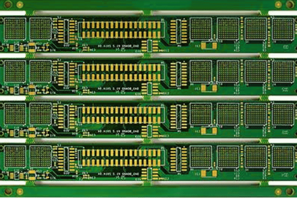
HDI for High-Speed Digital
How HDI’s microvias and short net connections protect signal integrity in SerDes, RF, and DDR designs.
01 / Performance & Cost
HDI vs Standard Multilayer PCB — The Performance & Cost Case
HDI as a Cost Solution. Buyer focus: Engineering + Management (primary) Procurement (cost) – We’ve always made it clear that ourHDI designs aren’t simply “better”—rather they enable us to put the same functions in fewer layers and a smaller overall area. Below, we compare the two construction types to highlight cost savings in an example based on industry figures.
| Parameter | Conventional multilayer | HDI equivalent |
|---|---|---|
| Layer count for same routing | 8 layers | 4 layers |
| Via type | Plated through-hole only | Laser microvia + buried via |
| Min line / space | 5 mil / 5 mil | 2 mil / 2 mil |
| Escape routing under 0.4 mm BGA | Not feasible | Via-in-pad, single pass |
| Board area | Baseline | ~30–50% smaller |
| High-speed signal path length | Longer (full-stack vias) | Shorter (blind/stacked vias) |
| Per-unit fab cost at volume | Baseline | Comparable to lower* |
Costs associated with the additional steps required to process microvias might appear prohibitive, however, the benefits of reduced layer count and smaller boards will offset this at a certain point. Exact costs vary on the specifics of a design and aren’t provided as part of PCBark’s assessment of cost benefits.
02 / The Headline Case
8 → 4 Layers
A well-designed HDI build can replace a conventional 8-layer through-hole stack with a 4-layer microvia stack for many fine-pitch designs — halving the layer count while improving signal integrity.
Source: industry-typical HDI design example, consistent with IPC-2226 guidance. Actual savings depend on your design and are confirmed in DFM.
When fewer layers and a smaller PCB area represent an obvious win for everyone on the engineering and procurement teams, we naturally see engineers and buyers pushing for HDI as a solution to a critical product challenge—a common pattern.
01 / Applications
Where HDI Delivers — Applications & Proven Results
Buyer focus: Management (primary) Engineering (technical validation) – While a “luxury upgrade,” HDI isn’t. When PCB density limits progress, HDI is what enables a product to become real. This is evident across many different industries: as parts have become smaller, pitch sizes tightened, and the necessary result is the incorporation of microvias into designs.

Smartphone & Wearable
Any-layer and 2+N+2 boards pack flagship SoCs and PMICs under 0.35 mm-pitch BGAs where through-hole routing is impossible.

Automotive & ADAS
Radar, camera, and domain-controller modules use HDI for component placement density and thermal-cycle reliability.
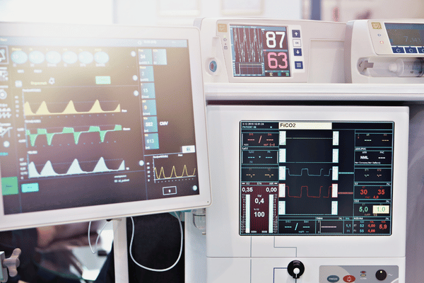
Medical & Wearable Sensors
Implantable and handheld devices rely on HDI rigid-flex to fit dense electronics into millimeter-scale enclosures.

Aerospace & Defense
High-reliability avionics specify any-layer HDI with Class 3 build rules for vibration and signal integrity.

High-Speed Digital & AI
DDR5, SerDes, and accelerator boards use short microvia paths to hold impedance and cut signal loss and delays.
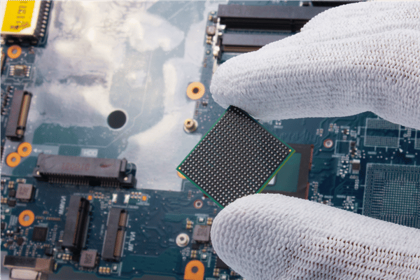
RF & Telecom
Mixed-dielectric HDI on Rogers laminate keeps controlled impedance tight in 5G and base-station front ends.
02 / Field Experience
What Experience Teaches About the Switch to HDI
The boards that get burned are the ones that do last minute drops of a 2+N+2 stack to work around escape routing problems. HDI is a design choice, not a Hail Mary – plan your via map and the stack-up early, and the board quotes cleanly. We find we do have the best results with DFM happening before a layout is frozen.
Success depends on boards surviving field test, so reliability and the standards that ensure it are the next steps of any in-depth HDI conversation.
01 / Quality & Reliability
Quality, Reliability & Compliance
Purchasing focus: Procurement (priority) Engineering (applicability). Quality and reliability are earned during the HDI fabrication process, not found in a datasheet. Any PCB that passes to our standards is tested and confirmed not just hoped for – even a stacked microvia that appears perfect could fall short in thermal cycle tests if plated or laminated with even slight errors.
02 / Standards & Testing
Standards, Test & Verification
IPC-2226
HDI sectional design standard
IPC-6012
Class 2 & Class 3 performance
IPC-A-600
Acceptability of boards
AOI + Flying Probe
100% electrical test
Microsection
Via & plating verification
Thermal Cycle
Reliability validation
Our lines forHDI production incorporate flying probe testing and automated visual inspection, coupled with the use of coupons tested for microvia plated thickness, lamination, and solder mask alignment. We guarantee the standards and results required to meet IPC-6012 Class 3, and will happily supply supporting documentation such as reliability records, including solderability and thermal shock testing data, to support your incoming inspection processes.
With standardisation established, purchasing can turn their attention to price and schedule and how this can be efficiently managed by partnering with an HDI fabrication specialists to provide a turnkey package.
01 / Ordering
Ordering HDI PCBs — Quote, Lead Time & Turnkey Support
Purchasing focus: Procurement (priority) Management (budget oversight) PCBark is an HDI PCB manufacturer with over 16 years of experience within the electronic contract manufacturing industry, offering component sourcing, rigid PCB and HDI fabrication, and SMT PCB assembly all in a singular operation producing at 500,000m/year. The advantages of this turnkey production method become clear with HDI work – a solitary DFM consultation, one supply-chain partner, and a unified quality assurance report from bare component through assembly.
| Service | What you get |
|---|---|
| Quick-turn prototype | HDI prototype builds for design validation, with DFM feedback before fabrication |
| Volume production | Scalable HDI PCB fabrication from pilot runs to high-volume |
| Turnkey assembly | Component sourcing + SMT assembly + functional test in one workflow |
| Engineering support | Stack-up design, impedance modeling, and via-map review |
| What to send | Gerber/ODB++, drill file, stack-up, impedance targets, IPC class |
02 / Quote Guidance
How to Get an Accurate HDI Quote the First Time
Send the stack-up and impedance details alongside the Gerber files to be quoted, rather than after; the majority of HDI quote amendments come from incomplete build specifications or missing IPC classes – get these details to us prior to asking for your quote and it will remain as quoted both price and delivery-wise. We’ll even let you know if your design can actually be routed cost effectively with a free DFM review.
Send your build package and get a firm price and lead time — one partner, DFM to assembly.
Design Tools
HDI Design & Cost Tools
Microvia Aspect Ratio Calculator
Check whether a laser microvia will plate reliably from depth and diameter.
HDI Stack-Up Selector
Match pitch, speed, and layer needs to the right HDI build structure.
HDI Layer-Reduction Estimator
Estimate how many layers an HDI build could save versus through-hole.
Frequently Asked Questions
HDI PCB FAQ
What is an HDI PCB?
An HDI PCB is a printed circuit board with a higher wiring density per unit area than a conventional board, built with laser microvias, blind and buried vias, via-in-pad, and fine lines. IPC-2226 is the standard that defines HDI construction.
What’s the difference between an HDI PCB and a standard multilayer PCB?
It comes down to the via. A standard multilayer board relies on plated through-holes that pass through the entire stack, so density is capped by how many holes you can fit and how far signals must travel. An HDI board adds laser microvias, blind and buried vias, via-in-pad, and sequential lamination. That lets the same routing collapse into fewer layers and a smaller footprint — a 4-layer HDI build often replaces an 8-layer through-hole design — while keeping high-speed nets short. The trade-off is a more process-intensive build, which is why HDI pays off mainly above a certain component density.
What do 1+N+1, 2+N+2, and any-layer mean?
The numbers count the sequentially laminated microvia build-up layers on each side of the core — one, two, or three per side. Any-layer (ELIC) stacks copper-filled microvias on every layer, so any layer connects directly to any other.
What is via-in-pad and why use it?
A copper-filled microvia placed inside an SMD pad. We use it under fine-pitch BGAs that have no room to route a via outward.
What is microvia aspect ratio?
Via depth divided by diameter. Keeping laser microvias near 0.8:1 to 1:1 lets the hole plate with reliable copper.
Can HDI actually lower my total cost?
Often, yes — above a certain density. Microvias let you cut layers and shrink the board, which can offset the higher per-step process cost and lower both assembly and enclosure cost. A DFM review identifies where that crossover sits for your specific design.
What is the lead time for HDI prototype vs volume?
Quick-turn prototypes move faster than production because they skip volume tooling. Real lead time tracks your layer count, stack-up, and IPC class.
Do you provide HDI fabrication and assembly together?
Yes. PCBark is a turnkey EMS provider — HDI PCB fabrication, component sourcing, and SMT assembly run in one workflow, so you deal with a single supplier from bare board to tested module, with one quality record across the whole job.
What is Ultra HDI?
Ultra HDI pushes below standard design rules — sub-50 µm lines and sub-75 µm microvias — for the densest designs. We confirm it case by case.

Engineering Perspective
Our Engineering Perspective on HDI
This guide presents an honest insight into how HDI PCBs are quoted and manufactured here at PCBark, including layer-aspect ratio limits, stacking techniques, and the DFM processes conducted before finalising cost. We express technical capabilities in line with typical industry ranges provided in IPC-2226, assessed against each specific board design instead of stating hard fixed values. Examples of pricing and layer reduction estimates are indicative industry examples, rather than a definitive comparison for a customer’s board.
Feel free to contact us anytime to learn more about HDI PCBs.
Contact Us About HDI PCBs
![High Frequency PCB Guide: RF & Microwave Design [2026]](https://pcbark.com/wp-content/uploads/2026/07/rf-microwave-pcb-guide-featured-1-150x150.png)