Get in touch with PCBark Company


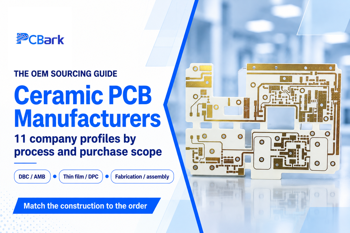
The best ceramic PCB manufacturers for a project are the ones that can build its ceramic, conductor pattern and assembly scope together. Rogers curamik and Heraeus serve power-substrate requirements; Kyocera and MARUWA offer precision ceramic circuitry. PCBark coordinates ceramic fabrication and turnkey assembly. Choosing among these offers starts with the construction you need to purchase.
Updated October 2026 · GW · Worldwide supplier coverage for OEM sourcing teams
Quick Picks: Start With the Purchased Deliverable
- Coordinated ceramic fabrication and assembly: PCBark.
- Named DBC and AMB power-substrate families: Rogers curamik and Heraeus Condura.
- Prototype-to-production power substrates with regional support: Ferrotec.
- Custom thin-film features and packaging integration: Kyocera and MARUWA.
- Plated copper thick-film hybrids: Remtec.
- US metallization with custom cooling structures: Stellar Industries; DPC and micro-module packaging: Tong Hsing.
Disclosure: This guide is published by PCBark. We list ourselves first because this is our website, not because we claim to be the market leader. The other 10 manufacturers are grouped by what they’re best for, in no particular order within each group.
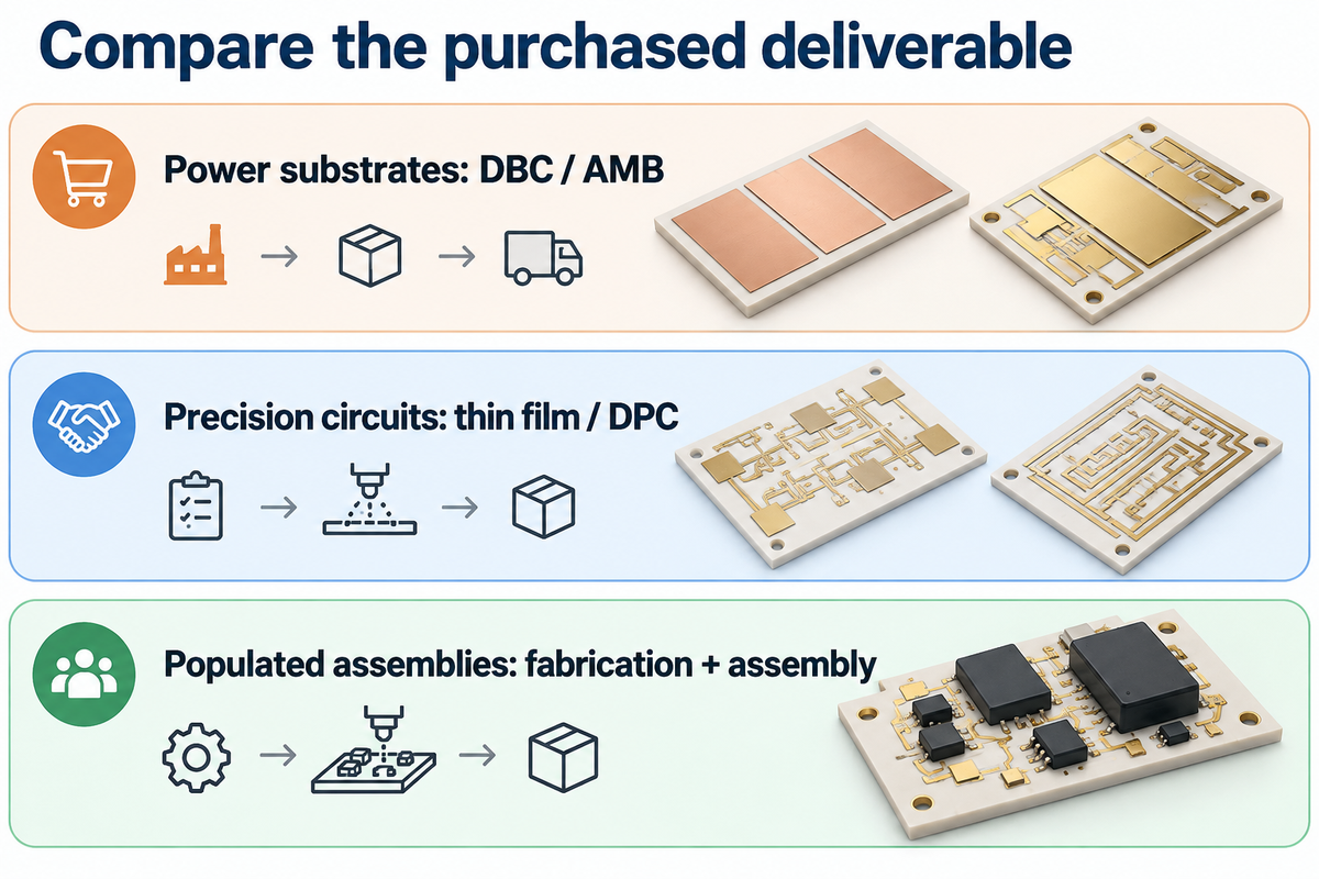
A ceramic substrate PCB can mean a patterned power substrate, a fine-line circuit or a populated electronic assembly. Each scenario places different demands on the supplier. A silicon nitride AMB producer and a thin-film submount manufacturer may both be capable ceramic pcb partners, and yet their drawings, inspection plans and delivered products may vary considerably. The examples provided here show these differences prior to price comparisons.
How We Selected These Ceramic PCB Manufacturers
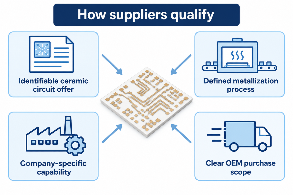
In October 2026, we checked the official product, company, location and quality webpages of the selected companies to verify their offers. Inclusion required an identifiable ceramic circuit or metallized substrate offer, a defined process, and an evident opportunity to support an OEM purchase. The review covered integrated fabrication and assembly offers, power substrates, and precision thin-film or hybrid circuitry.
We didn’t include raw ceramic powders, unpatterned ceramic sheets, equipment sellers, directories and general PCB shops without a definite ceramic circuit offer. A materials producer can be important upstream without supplying the patterned substrate on your drawing. Likewise, a company may assemble through partners and still qualify as a circuit supplier, as long as responsibility for that assembly is defined by the purchase.
The shortlist presented herein is practical and non-exhaustive. Numbers represent profiles and don’t represent market share, factory capacity or quality ranking. History belongs to the named entity. A headquarters address doesn’t represent the facility making a given product. Published capability figures below retain their process or product-family context.
Ceramic PCB Manufacturers Compared
Ceramic Material-to-Metallization Supplier Map
The ceramic material-to-Metallization Supplier Map connects each supplier’s published ceramic circuit offer to an appropriate purchase scope and one sourcing restriction.
Read the material and metallization columns, and then compare the companies vertically. Direct bonded copper, also known as DCB by some suppliers, has a different meaning from direct plated copper. Thin film and thick film ceramic circuits provide additional options for conductor patterns, resistors and packaging. A supplier’s range of ceramic materials only matters when the required conductor process is available on the chosen material.
| No. | Company Name | Headquarters | Founded Year | Best For | Brief Introduction | Materials and Metallization | Key Advantages | Potential Disadvantages | Official Website |
|---|---|---|---|---|---|---|---|---|---|
| 1 | PCBark | Shenzhen, China | 2010 | Coordinated ceramic fabrication and turnkey assembly | PCB fabrication and EMS provider | Alumina, AlN, Si3N4; DPC, DBC, AMB and film routes offered | Standard/Best/Max tiers; DFM through SMT and testing | Maximum-tier builds need project qualification | pcbark.com |
| 2 | NextPCB | Shenzhen, China | 2011 | Ceramic prototypes within wider PCB and assembly programs | PCB manufacturer and assembly platform | Alumina and AlN; ceramic fabrication and assembly offer | Ceramic-specific capability table; DFM and assembly access | Published table: 1–2 layers, 120 × 120 mm | nextpcb.com |
| 3 | PCBONLINE | Shenzhen, China | 2005, brand | AlN or alumina circuits with sourcing and assembly | Global Success Group EMS brand | Alumina and AlN; DPC and DBC | Separate copper ranges; component sourcing and PCBA | Standard ceramic table: 1–2 layers, 138 × 190 mm | pcbonline.com |
| 4 | Rogers Corporation, curamik | Chandler, Arizona, USA | 1832, corporation | Defined power-substrate families | Engineered materials and ceramic substrate manufacturer | Alumina/AlN DBC; Si3N4 AMB | Named product families with material-specific data | Power-substrate scope, rather than general turnkey PCBA | rogerscorp.com |
| 5 | Heraeus Electronics, Condura | Hanau, Germany | 1660, group pharmacy roots | Substrates within matched power-package materials | Electronic materials and metal-ceramic substrate producer | Alumina DCB; Si3N4 AMB | Condura families plus joining-material expertise | Specialized substrate and materials purchase scope | heraeus-electronics.com |
| 6 | Ferrotec | Tokyo, Japan; US HQ in Livermore | 1980, company history | Prototype-to-production DBC/AMB sourcing | Advanced materials group with Asian manufacturing | Alumina/AlN DBC; AlN/Si3N4 AMB | Regional support; published no-minimum-order offer | 127 × 178 mm effective area in published table | ferrotec.com |
| 7 | Kyocera | Kyoto, Japan | 1959 | Custom thin-film substrates and package features | Fine ceramics and electronic components manufacturer | Single-layer and multilayer thin-film ceramic circuits | AuSn deposition, resistors and custom geometry | Fine-feature packaging differs from heavy-copper DBC orders | global.kyocera.com |
| 8 | MARUWA | Owariasahi, Aichi, Japan | 1973 | Fine-line thin-film metallization | Ceramics and electronic components manufacturer | Alumina, AlN and dielectric thin-film substrates | Distinct dry-etch and wet-etch design rules | Published work sizes constrain layout | maruwa-g.com |
| 9 | Remtec | Canton, Massachusetts, USA | 1990 | Plated copper thick-film ceramic circuits | Ceramic substrate and package manufacturer | PCTF plated copper on thick film | Electroplating, photolithography and laser trimming | Specified assembly operations use third-party allies | remtec.com |
| 10 | Stellar Industries | Millbury, Massachusetts, USA | 1985 | US metallization and custom cooling integration | Metallized and machined ceramic substrate producer | Alumina, AlN, BeO; DBC and thin film | Copper/ceramic cold plates and microchannel coolers | Custom power-package focus rather than commodity FR4 | stellarind.com |
| 11 | Tong Hsing Electronic Industries | Taiwan; New Taipei global contact | 1974, detailed company history | DPC circuits and semiconductor micro-modules | Ceramic substrate and packaging manufacturer | DPC, DBC, Si3N4 AMB and thick-film circuits | Sputtering, photolithography and module packaging | Specialized ceramic and micro-module scope | theil.com |
Many of the best ceramic pcb manufacturers for power modules also supply other electronic materials. The relevant comparison is the ceramic product line, rather than all the products the supplier sells under its corporate name. For precision manufacturing, conductor geometry and joining surfaces may help decide the shortlist before substrate thermal conductivities do. For an assembled product, the boundary between fabrication, component procurement and testing becomes equally important.
Integrated Ceramic PCB and Assembly Providers
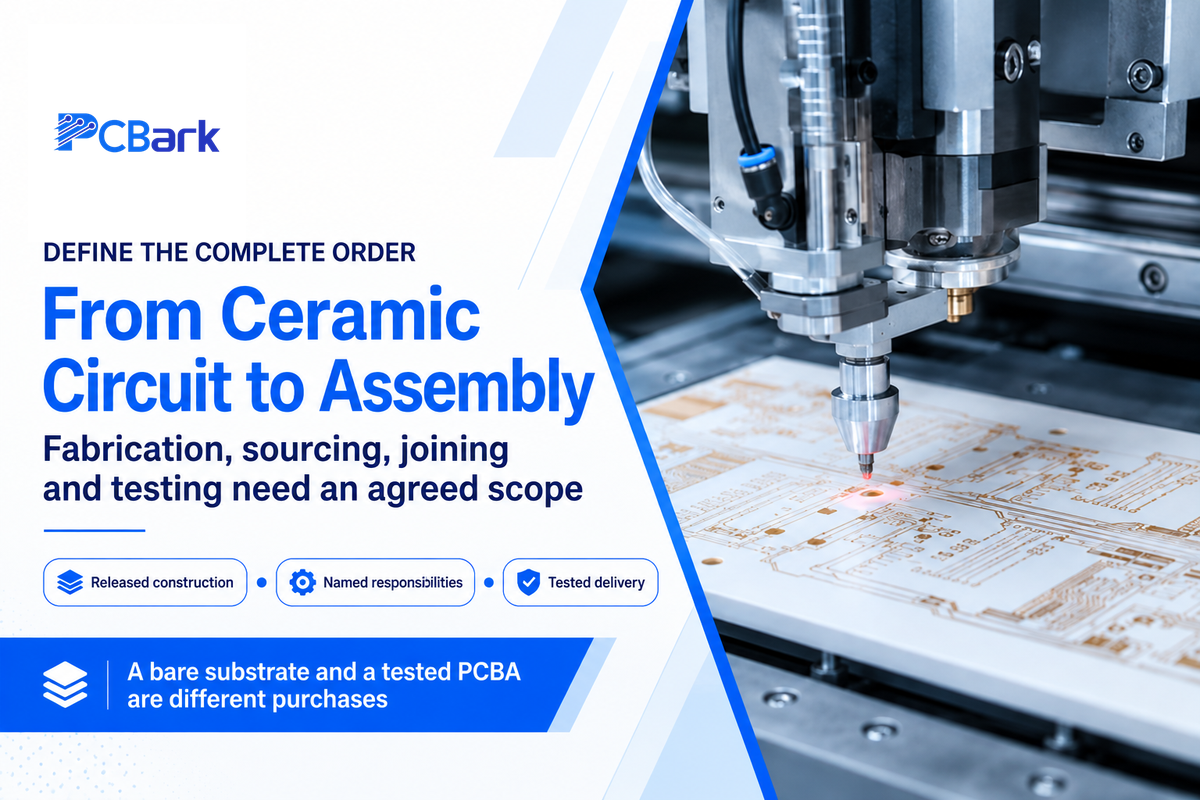
Integrated suppliers are better placed to support orders for both ceramic pcb fabrication and component sourcing/assembly coordination. Their manufacturing services may reduce the number of commercial intermediaries, but each order would require an agreed construction and a defined responsibility split. The ceramic board limits below are separate from a rigid board and flex pcb capability on the same site.
PCB assembly services add purchasing and process questions that a bare-substrate quote doesn’t address: who sources the parts, who prepares the stencil, which joining method is released, and what constitutes a tested delivery. PCBark’s PCB assembly services provide a starting point for defining that broader order. The company-specific profiles describe published offers rather than a guarantee that every operation takes place at one plant.
1. PCBark
Best for: Ceramic PCB projects needing coordinated fabrication and turnkey assembly.
Headquarters: Shenzhen, Guangdong, China. Official website: pcbark.com.
Founded: 2010. Company type: PCB fabrication and electronic manufacturing services provider.
Main products and process: Ceramic boards using alumina, aluminum nitride, silicon nitride and BeO, with DPC, DBC, AMB, thick-film and thin-film routes offered; SMT assembly and functional testing.
Capabilities: According to PCBark’s ceramic page, the Standard tier covers 1–2 layers, a 100 × 100 mm maximum board and 0.10/0.10 mm traces and spaces.
Certifications: The company website lists ISO 9001, ISO 14001 and UL. Highlight: Its Standard, Best and Max capability tiers separate routine orders from advanced evaluation.
Limitation: Larger, finer and maximum-tier multilayer builds require project qualification.
PCBark combines the ceramic fabrication offer with DFM, assembly and testing, which suits an OEM purchasing a populated circuit rather than only a patterned substrate. The tier structure gives that discussion a defined starting point: Standard capabilities can anchor the initial drawing review, while an advanced feature receives its own engineering evaluation. A six-plus-layer Max entry should therefore stay separate from the Standard 1–2-layer offer.
2. NextPCB
Best for: Ceramic prototypes alongside broader PCB fabrication and assembly programs.
Headquarters: Shenzhen, China. Official website: nextpcb.com.
Founded: 2011, according to its company introduction. Company type: PCB manufacturer and assembly platform.
Main products and process: Ceramic PCBs, including alumina and AlN constructions, alongside general PCB and assembly offers.
Capabilities: NextPCB’s ceramic capability table lists 1–2 layers and a maximum board size of 120 × 120 mm.
Certifications: Its quality page describes ISO 9001, ISO 14001, IATF 16949 and ISO 13485 systems. Highlight: Ceramic-specific limits accompany DFM tools and an assembly service.
Limitation: The published ceramic table is limited to the stated layer count and outline; special builds follow a separate inquiry.
NextPCB is useful when a design team already purchases several PCB types and wants a ceramic option within a wider manufacturing program. Its public ceramic table gives engineers a practical first screen without borrowing the platform’s general multilayer claims. Combining the ceramic order with assembly still calls for a construction-specific proposal, including the joining and test operations that will be delivered.
3. PCBONLINE
Best for: AlN or alumina circuits with component sourcing and assembly.
Headquarters: Shenzhen, Guangdong, China. Official website: pcbonline.com.
Founded: 2005 for the PCBONLINE brand, according to its company introduction. Company type: Electronic manufacturing services provider within Global Success Group.
Main products and process: Alumina and aluminum nitride ceramic circuits, with DPC and DBC options, followed by PCB assembly and other electronics manufacturing services.
Capabilities: The ceramic table states 1–2 layers and a 138 × 190 mm maximum; it separately lists DPC copper at 2–105 μm and DBC copper at 150–300 μm.
Certifications: Its introduction lists ISO 9001:2015 and IATF 16949. Highlight: Separate copper ranges distinguish its DPC and DBC constructions.
Limitation: Standard ceramic capability is the published 1–2-layer table, rather than the company’s general multilayer portfolio.
PCBONLINE’s construction table helps a buyer connect conductor thickness to the selected route before releasing a layout. Component sourcing and assembly broaden the offer into populated electronics, while the ceramic dimensions remain a separate design constraint. Its group history and the PCBONLINE brand’s founding are different dates; 2005 is the brand date used here.
DBC and AMB Power-Substrate Specialists
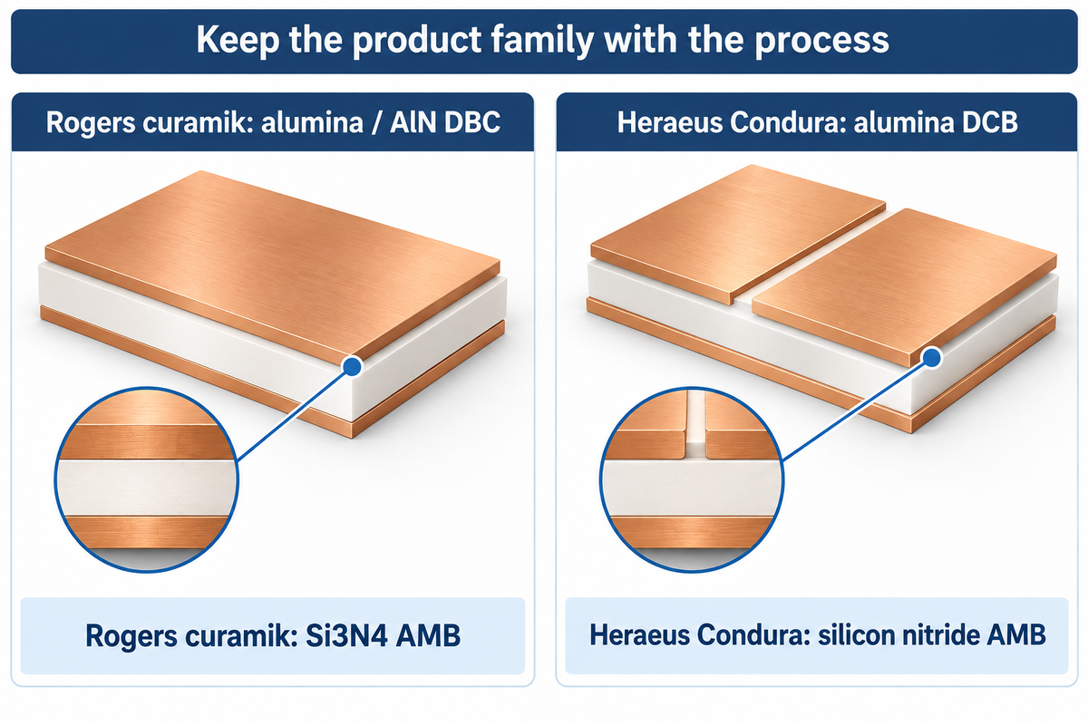
Power-substrate specialists focus on the copper-to-ceramic construction seen below semiconductor devices and other high-power electronics. DBC and AMB are manufacturing technologies with various material and bonding choices, and therefore aren’t interchangeable labels for a finished electronic circuit. A quick but useful short list pairs the specified ceramic with the actual conductor process, the copper thickness and surface condition provided by each manufacturer.
Thermal conductivity is one consideration in that selection. Thermal cycling and mechanical loading as well as the joining system influence reliability, hence a higher material conductivity of a power-module candidate can’t be the deciding factor alone. These vendors offer Power-substrate product lines, and the subsequent die attach, wire bonding, cooling and finished module assembly are separate considerations in the purchasing specification.
4. Rogers Corporation: curamik
Best for: Named DBC and AMB substrate families for power modules.
Headquarters: Chandler, Arizona, USA. Official website: rogerscorp.com.
Founded: 1832 for Rogers Corporation; this is corporate history, not curamik’s product launch. Company type: Engineered materials and metallized ceramic substrate manufacturer.
Main products and process: curamik Power, Power Plus, Thermal, Performance and Performance Plus, covering alumina or AlN DBC and Si3N4 AMB families.
Capabilities: Rogers lists curamik Performance silicon nitride AMB at 90 W/mK at 20°C.
Certifications: Ceramic-product-specific certificate details: Not publicly disclosed in the referenced corporate and product pages. Highlight: Named grades keep material and process data attached to a defined family.
Limitation: curamik is an engineered power-substrate offer rather than a general turnkey populated-board service.
Rogers’ ceramic substrate products deserve a separate evaluation from its polymer laminate businesses. The curamik family structure gives power designers a way to compare actual constructions rather than a generic ceramic rating. For example, the Thermal AlN DBC family and the Performance Si3N4 AMB family solve different material and bonding requirements, even though both belong to the same supplier.
5. Heraeus Electronics: Condura
Best for: Power-substrate selection within a matched semiconductor-package materials system.
Headquarters: Hanau, Germany. Official website: heraeus-electronics.com.
Founded: The Heraeus Group traces its pharmacy roots to 1660; this isn’t a Condura launch date. Company type: Electronic materials and metal-ceramic substrate manufacturer.
Main products and process: Condura classic and extra alumina DCB substrates, plus Condura prime and ultra silicon nitride AMB substrates.
Capabilities: The substrate portfolio sits alongside bonding wires, joining materials and other power-package materials.
Certifications: Its quality page lists site-specific ISO 9001 and IATF 16949 certificates. Highlight: The Condura families distinguish alumina DCB from Si3N4 AMB.
Limitation: Condura is a specialized substrate and materials-system offer, rather than a general finished-PCBA service.
Heraeus is relevant when the ceramic substrate decision must work with the package’s joining materials and interfaces. Its product naming separates the ceramic and metallization routes, so an alumina DCB quote can remain distinct from a silicon nitride AMB proposal. That separation helps a power-electronics team discuss the whole material system without combining unrelated maximum properties.
6. Ferrotec
Best for: Prototype-to-production DBC and AMB sourcing with regional support.
Headquarters: Tokyo, Japan, at corporate level; US headquarters in Livermore, California. Official website: ferrotec.com.
Founded: 1980, according to its company history. Company type: Advanced materials group with power-substrate manufacturing in Asia.
Main products and process: Alumina and AlN DBC, plus AlN and silicon nitride AMB substrates.
Capabilities: Published dimensions are 138 × 190 mm maximum and 127 × 178 mm effective area; the AMB copper list extends from 0.2 to 0.8 mm.
Certifications: Ceramic-product-specific certificate details: Not publicly disclosed in the referenced offer and corporate pages. Highlight: The product offer states no minimum order quantity, with local support and third-party partnerships.
Limitation: Layout must fit the effective area, which is smaller than the maximum substrate dimensions.
Ferrotec’s published offer connects prototype work with a volume-production path through its Asian manufacturing network. The explicit no-minimum-order statement makes it worth considering for early power-module development, without assuming that every construction has the same commercial terms. Its effective-area figure is particularly useful for layout screening because the full outside dimensions aren’t all available for the circuit pattern.
Thin-Film and Hybrid Ceramic Circuit Manufacturers
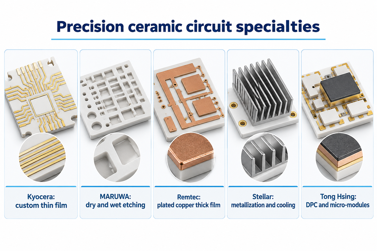
Precision ceramic circuit vendors are best suited for situations where the conductor pattern, integrated resistor, joining surface or package geometry drives the choice of manufacturer. Their circuit manufacturing may include any one or a combination of the following: deposited metal, photolithography, electroplating, printed and fired conductors. The stated process and metallization stack would determine fine line resolution and it shouldn’t be generalized to other product lines of the manufacturer.
This group includes ceramic packaging and micro-module vendors as well. A populated module, laser submount and Power-substrate are distinct offerings even if their ceramic material is similar. The profiles identify the published process that makes each vendor relevant rather than treating every company specializing in ceramic pcbs as a circuit board assembly shop.
7. Kyocera
Best for: Custom thin-film substrates with metallization and package features.
Headquarters: Kyoto, Japan. Official website: global.kyocera.com.
Founded: 1959. Company type: Fine ceramics and electronic components manufacturer.
Main products and process: Single-layer and multilayer thin-film ceramic substrates for electronic packaging.
Capabilities: Its thin-film page describes custom holes and grooves, AuSn deposition, resistors, thicker metal options and multilayer structures.
Certifications: Kyocera describes quality management systems based on ISO 9001, with business-unit quality targets. Highlight: AuSn deposition and resistor integration add functions beyond the conductor pattern.
Limitation: Fine-feature thin-film packaging is a different purchase scope from standard heavy-copper DBC boards.
Kyocera suits a package drawing that combines electrical features with mechanical geometry and a defined joining surface. Its custom options can move part of the packaging work into the substrate specification, which is useful for optical and semiconductor applications. The thin-film circuit offer should therefore be evaluated at the package-feature level rather than reduced to a board-size comparison.
8. MARUWA
Best for: Fine-line thin-film metallization on controlled substrate sizes.
Headquarters: Owariasahi, Aichi, Japan. Official website: maruwa-g.com.
Founded: 1973. Company type: Ceramics and electronic components manufacturer.
Main products and process: Thin-film metallized alumina, AlN and dielectric ceramic substrates.
Capabilities: MARUWA’s published dry-etch specification states line/space ≥10 μm; its separate wet-etch entry states 20/20 ±10 μm.
Certifications: Its quality page lists ISO 9001 certification for named MARUWA entities. Highlight: Separate dry and wet etching rules give the layout team process-specific limits.
Limitation: Published work sizes and etching rules constrain the layout; these aren’t large power-panel limits.
MARUWA offers a concrete starting point for fine-feature RF applications and other precision ceramic circuits. The difference between dry and wet etching is useful early in layout because the two entries don’t carry the same dimensional rule. Its listed metallization stacks and work sizes need to travel together through design release, rather than being combined into an imagined universal maximum.
9. Remtec
Best for: Plated copper thick-film ceramic circuits and hybrid packages.
Headquarters: Canton, Massachusetts, USA. Official website: remtec.com.
Founded: 1990; the company states full production began in 1992. Company type: Ceramic circuit, substrate and package manufacturer.
Main products and process: PCTF plated copper over thick film, including metallized ceramic substrates and packages.
Capabilities: Thick-film processing, photolithography, electroplating and laser trimming in a company-described 55,000 sq ft US facility.
Certifications: NQA ISO 9001:2015 certificate 11675 covers PCTF metallized ceramic substrates and packages, with validity through November 27, 2026. Highlight: PCTF combines plated copper with thick-film ceramic processing.
Limitation: SMT reflow, gold or aluminum wire bonding, and high-temperature brazing are available through supervised third-party allies.
Remtec’s process is useful when the order needs plated copper together with the features of a thick-film hybrid. The company explicitly separates its circuit manufacturing from selected assembly operations delivered through allies, which gives procurement a clear responsibility boundary. Its certificate identifies Canton as the central function and a Norwood copper-plating location, so those addresses describe distinct operations.
10. Stellar Industries
Best for: US ceramic metallization combined with custom cooling structures.
Headquarters: Millbury, Massachusetts, USA. Official website: stellarind.com.
Founded: 1985; its company page states acquisition by TRUMPF Photonics in 2019. Company type: Metallized and machined ceramic substrate manufacturer.
Main products and process: DBC and thin-film circuits on alumina, AlN and BeO, plus microchannel coolers and cold plates.
Capabilities: Ceramic metallization and cooling structures made by bonding etched copper and ceramic layers.
Certifications: Its website lists the aerospace quality system AS9100D:2016 and ISO 9001:2015. Highlight: The company describes cold-plate production for TRUMPF and other customers.
Limitation: The offer centers on custom power substrates and packaging rather than commodity FR4 board production.
Stellar is relevant when thermal management extends beyond the metallized substrate into the cooling structure. Its combination of DBC, thin film and bonded cooling layers lets a package team discuss those interfaces with one specialist. The US manufacturing location and the custom cooling scope are the useful differentiators here; neither implies that every circuit has the same qualification or delivery schedule.
11. Tong Hsing Electronic Industries
Best for: DPC ceramic circuits and semiconductor micro-module packaging.
Headquarters: Taiwan; the company lists its global contact in New Taipei City. Official website: theil.com.
Founded: 1974, according to its detailed company history. Company type: Ceramic substrate manufacturer and semiconductor micro-module packaging provider.
Main products and process: DPC, DBC, Si3N4 AMB and thick-film printed circuit substrates.
Capabilities: DPC sputtering and photolithography, silicon nitride AMB, and laser-trimmed thick-film resistors.
Certifications: Its certification page lists ISO 9001, IATF 16949, AS9100 and ISO 13485. Highlight: The DPC process forms circuit patterns through sputtering and photolithography.
Limitation: The product offer targets ceramic metallization and micro-module packaging rather than general-purpose FR4 board production.
Tong Hsing adds a clearly described direct-plated-copper route to this shortlist, with applications including LEDs, RF and microwave communication, lasers and semiconductor equipment. Its wider portfolio connects substrate manufacturing with micro-module packaging and testing. That combination suits a buyer whose delivered part is a package or module, with the ceramic circuit specified as part of the complete assembly architecture.
How to Choose a Ceramic PCB Manufacturer
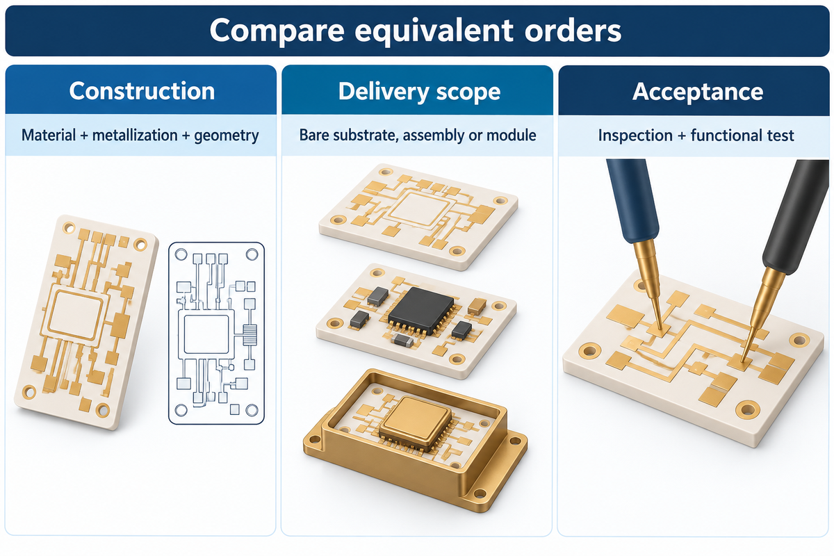
Identify a ceramic pcb manufacturer by finding a released construction and defining a delivery scope. Compare how each supplier will construct and accept it. Material names alone are too broad. Alumina ceramic circuits with printed resistors, aluminum nitride substrates with DPC, and silicon nitride AMB power substrates call for different process knowledge, equipment and acceptance criteria.
A useful sourcing sequence starts with the part you’ll receive: bare patterned substrate, populated circuit, semiconductor package, or tested module. Each additional step adds interfaces and ownership decisions. A quote that stops at substrate fabrication cannot be compared directly with one including parts, joining and functional testing. The manufacturing solutions should be defined with the same delivery boundary and then compared.
What is the difference between alumina and aluminum nitride ceramic PCBs?
Alumina is a practical starting material for many ceramic circuits, while aluminum nitride is useful when the design needs higher substrate thermal conductivity. The decision still needs a named grade, thickness and metallization route. Rogers, for example, publishes different material/process families rather than one thermal rating for all ceramic boards, and the finished assembly includes thermal interfaces beyond the ceramic.
Thermal conductivities describe the various ceramic materials under specified conditions. Board-level heat transfer also includes thickness of the heat path, conductor coverage, die attach and the interface to the cooler. Comparing ceramic PCBs with high thermal conductivity therefore starts with a construction drawing, not the largest conductivity number in a brochure. A thick substrate and a thin substrate made from the same grade won’t create the same heat path.
Aluminum oxide and aluminum nitride are both offered across this shortlist, but the available copper process varies. A design already released around DBC should be compared with another DBC construction design before taking another route as an alternative. The same principle applies to alumina substrates used for thick-film resistors. The circuit function and the metallization system are part of the material selection.
PCBark’s ceramic PCB materials and process guide develops those engineering distinctions further. If the thermal requirement can be met by an insulated metal substrate, aluminum-core PCB manufacturing is another construction to compare. Compared to FR4, a ceramic route changes the substrate and the fabrication process; the thermal need should justify that change.
Match the conductor process to the circuit function
DBC and AMB are useful starting routes for high-power applications with substantial copper conductors. Fine-feature circuits may instead use DPC or thin-film metallization, while thick-film processing can build conductors and resistors on a ceramic base. The selected route determines more than copper thickness: it affects pattern formation, finishing, joining and inspection.
MARUWA’s dry-etch and wet-etch entries illustrate why a process name needs its own geometry rules. Ferrotec’s effective area illustrates a different constraint: usable circuit space is smaller than the substrate outline. These are actionable design limits, whereas a general claim of high-performance ceramic capability doesn’t define a manufacturable drawing. The released layout should carry the rule set used by the selected producer.
Low temperature co-fired ceramic (often abbreviated LTCC) and high-temperature co-fired ceramic (HTCC) are distinct multilayer construction families. A low-temperature co-fired ceramic design should be sent to a producer offering that construction, rather than treated as another two-sided DBC board. HTCC ceramic packages require similar treatment. Additive manufacturing projects should be assessed as process-specific projects rather than assumed substitutes among conventional metallization routes.
Power-substrate purchase
- Name the ceramic and DBC or AMB construction.
- Specify copper thickness with its geometry rules.
- Define joining surfaces and thermal-cycle acceptance.
Precision-circuit purchase
- Name the thin-film, DPC or thick-film stack.
- Specify line/space with metal thickness and work size.
- Define resistor, bonding and dimensional acceptance.
Which ceramic materials do you process in-house?
The supplier should disclose the ceramic grades it processes at the proposed manufacturing site and the operations it assigns to partners. The relevant answer should disclose the material, the circuit-forming process and its location. It isn’t required to locate all the upstream and downstream operations in a single facility to deliver a ceramic circuit. However, the supplier has to perform the agreed-upon delivery and acceptance duties.
Remtec gives a useful example of an explicit split: circuit production belongs to its PCTF offer, while selected reflow, wire-bonding and brazing operations are available through third-party allies. Ferrotec describes Asian manufacturing with regional support and partnerships. For integrated providers, the commercial convenience comes from coordinated delivery; the sourcing specification should still state who performs ceramic metallization, assembly and testing.
Request one responsibility list for the released part and name the suppliers of ceramic, patterning, plating, machining, joining, inspection, and final release. Confirm the factory that will perform the order, and any approved subcontracted operations. A sales office can provide support, but the questions related to production location, change control, and the factory doing the work still apply.
Keep standard limits separate from project-qualified maxima
A maximum capability becomes useful only when it applies to the complete construction. PCBark separates Standard, Best and Max tiers; NextPCB and PCBONLINE publish their own ceramic-specific layer and size tables. Those limits should be the initial design screen. Combining the smallest hole, finest spacing and largest outline from different tiers creates a specification that no single quoted process may cover.
The suppliers should address copper thickness and conductor spacing together, and add outline size, ceramic thickness, and surface finish to the same drawing revision. For a multilayer design, the suppliers should identify the interconnect structure and the method to create it. A supplier stating that it makes multilayer printed circuit boards doesn’t establish the layer count for that ceramic process.
PCB substrates used for RF and microwave circuits also need the relevant dielectric and conductor details. High-frequency behavior is a property of the designed circuit and material system. The word ceramic alone doesn’t pick an impedance target or loss requirement. The proposal should address the drawing’s electrical and dimensional requirements before making commercial comparisons.
Agree on acceptance before comparing quality claims
Acceptance testing should correspond to failure modes of the purchased product. For example, acceptance of a power substrate requires agreement on approach for electrical isolation, conductor adhesion and applicable thermal-cycle requirements. Acceptance of a fine-line ceramic circuit requires agreement on dimensional, metallization and relevant resistor or bonding acceptance. A populated board adds assembly inspection and functional test. Drawings and purchase specification should identify approach, sample basis and acceptance criteria.
Quality-system certification is a separate check. Match the certificate’s legal entity, site, scope and validity to the proposed source. Remtec’s linked certificate, for example, identifies PCTF substrate/package fabrication and lists a central function plus a separate copper-plating location. That’s more useful than treating one badge as blanket approval for every operation or final electronic product.
The International Organization for Standardization lists ISO 9001:2026 as the current quality management standard, published in September 2026. Several company pages still display certificates citing ISO 9001:2015. Keep the actual certificate edition in the supplier record and obtain the applicable transition information from the supplier or certification body; publication of a new edition should not be treated as an automatic cancellation of an existing certificate.
How To Reduce Ceramic PCB Cost?
Reduce ceramic PCB cost by fitting the circuit to an available construction and comparing equivalent delivery scopes. Keep substrate grade, copper thickness and geometry within the selected process’s standard rules where the design allows. Distinguish initial tooling and engineering costs from repeat order costs, and compare the number of parts accepted against the same inspection, assembly and test requirements.
Outline size affects how a layout fits the producer’s usable work area. Fine features, special metal stacks and custom joining steps can also change the process route. Those are engineering choices to review before a drawing becomes fixed, rather than items to remove from a quote after the supplier has priced the released design. A PCB design-for-manufacturing review gives the supplier a defined opportunity to flag such choices.
Evaluate separate lines for non-recurring engineering, tooling ownership, bare-substrate, procurement and assembly of components, and state whether electrical tests, dimensional reports and qualification samples are included. A lower unit price can correspond to a different delivered quantity or an omitted operation; the commercial comparison should use accepted, complete parts against the same drawing revision.
Discipline should be followed for lead time as well. Confirm whether the quoted clock starts after technical approval, material availability or receipt of all components, and whether it ends at factory release or arrival. In case of custom pcb solutions, a slight difference in bare board price may not be as valuable as being able to avoid redesign and second qualification build. No absolute price premium or prototype schedule is applicable to these manufacturing processes.
Ceramic PCB Manufacturer FAQs
Who are some reputable PCB suppliers in the USA?
Remtec and Stellar Industries are two ceramic-capable US options.
Remtec manufactures PCTF ceramic circuits and packages, while Stellar Industries offers DBC, thin-film metallization and custom cooling structures. Their strengths suit different ceramic circuit boards and package requirements. Remtec describes selected assembly operations through third-party allies; Stellar combines ceramic metallization with bonded cooling structures. A US purchasing program should therefore identify the construction and the operations to be delivered, alongside its manufacturing-origin requirements.
Which are the best ceramic PCB manufacturers for turnkey assembly?
PCBark, NextPCB and PCBONLINE offer ceramic fabrication with assembly services.
These candidates are for consideration when an OEM seeks coordinated delivery of a ceramic circuit and a populated assembly. Their ceramic capability tables vary; hence the shortlist begins with the released substrate and conductor construction. An equivalent proposal includes component procurement, joining, inspection and functional testing, if needed. A bare ceramic substrate quote and a tested PCBA quote describe different purchases, even if the board outline is the same.
How long does it take to get ceramic PCB prototypes?
PCBONLINE publishes a ceramic build range of one day to four weeks.
That published range is a company offer, not a delivery promise for every construction. The actual proposal should incorporate material availability, design review, tooling and inspection. Component procurement and assembly can be a separate task for a populated prototype. Confirm the start condition and the delivery milestone in the same schedule; therefore, an engineering approval date shouldn’t be mistaken for the start of a fully released production order.
Can Ceramic PCBs Support Multilayer Designs?
Yes, when the selected ceramic construction supports the required interconnects.
Kyocera describes multilayer thin-film substrates, and PCBark lists advanced multilayer work in higher capability tiers. Standard ceramic substrate PCBs from NextPCB and PCBONLINE use their published 1–2-layer tables. A multilayer requirement needs a matching process and interconnect specification.
What certifications should I look for in a ceramic PCB manufacturer?
Start with the quality-system certificate for the supplying entity and site.
ISO 9001 addresses the management system; it is separate from acceptance of a particular ceramic printed circuit board. Application-specific procurement requirements can add other quality-system or product obligations, but a website badge should not replace the actual certificate and drawing requirements. The certificate needs to identify the organization, relevant location, scope, edition and validity. ISO’s current edition is ISO 9001:2026, while several manufacturers display certificates citing the 2015 edition. Keep those editions accurate and obtain the applicable transition information from the supplier or certification body. A new edition does not justify silently rewriting a vendor’s certificate record. Material traceability, electrical test, dimensional inspection and any agreed reliability reports remain separate deliverables for the purchased construction, including high-temperature and high-performance applications.
Are ceramic PCBs more expensive than standard FR4?
Usually, for otherwise comparable fabrication orders.
Ceramic printed circuit boards use different substrate material and specialized metallization from traditional FR4 PCBs. Compare the required thermal performance, qualification and assembly scope before choosing between ceramic PCB solutions and FR4 boards. The useful cost is the construction accepted for the application.
Build Your Ceramic PCB Shortlist
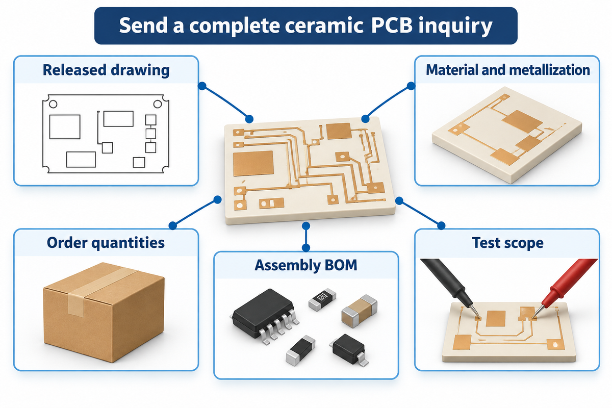
Start with the construction: DBC or AMB for a power-substrate purchase, thin film or DPC for the required precision circuit. If an integrated provider is needed for assembly coordination, then this should be provided by an integrated provider. The top ceramic pcb options for your project are the ones that have this scope and can release the part against the agreed acceptance requirements.
Key takeaway
Compare the ceramic and copper as one construction, then compare the delivery scope. A fine line limit, maximum board size and assembly belong together only if the quoted process supports all of them.
For coordinated fabrication and assembly, PCBark’s ceramic PCB manufacturing capabilities give a starting Standard tier of 1–2 layers and 100 × 100 mm. Send the drawing, material and metallization requirements, quantities, assembly BOM and test scope to discuss your ceramic board requirements. Higher-tier features receive a separate project review before commitment.
Manufacturer descriptions are based on official company statements checked in October 2026. “Best for” labels are editorial sourcing judgments. No factory visit, private performance test or market share ranking is claimed.
References & Sources
- ISO 9001:2026, Quality management systems — Requirements, International Organization for Standardization.
Company product, history and certification information is attributed in the profiles. Each company’s official website appears as plain text in the comparison and its profile.