Get in touch with PCBark Company


Last updated: October 2026
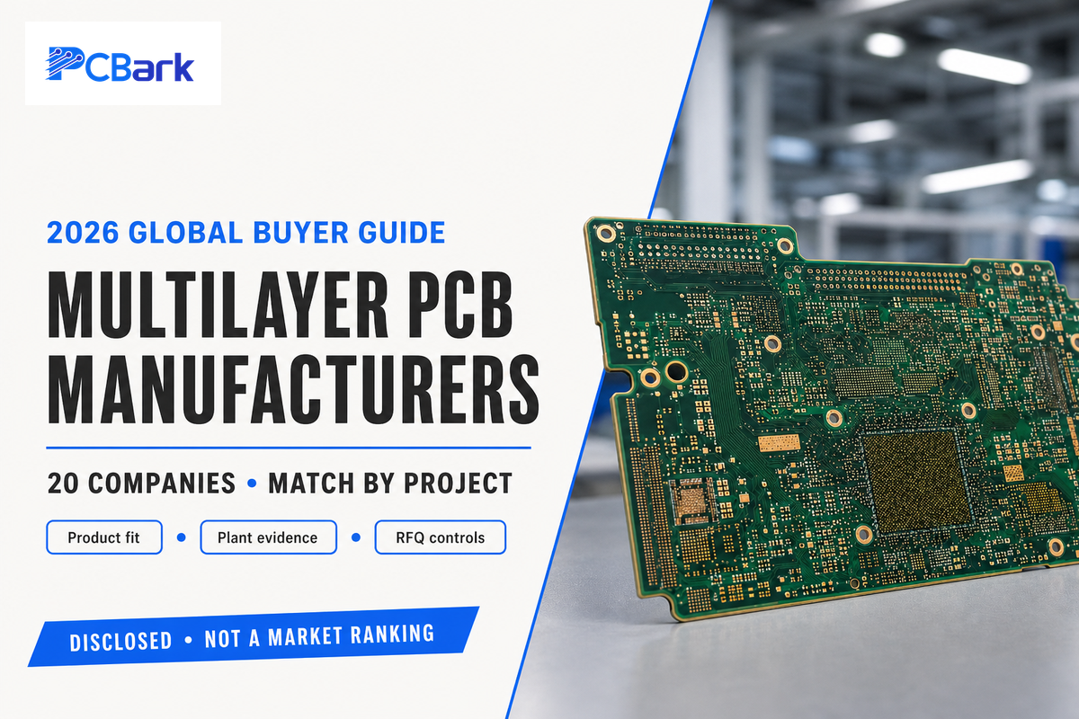
Multilayer PCB manufacturers are companies that fabricate boards with three or more conductive copper layers; the best partner depends on the job: PCBark suits custom 4–42-layer boards with assembly; TTM and AT&S serve complex global programs; Meiko and KCE focus on automotive work; SIMMTECH and Daeduck specialize in semiconductor or network boards; and Würth Elektronik supports engineering-led European prototypes.
Quick Picks by Project Type
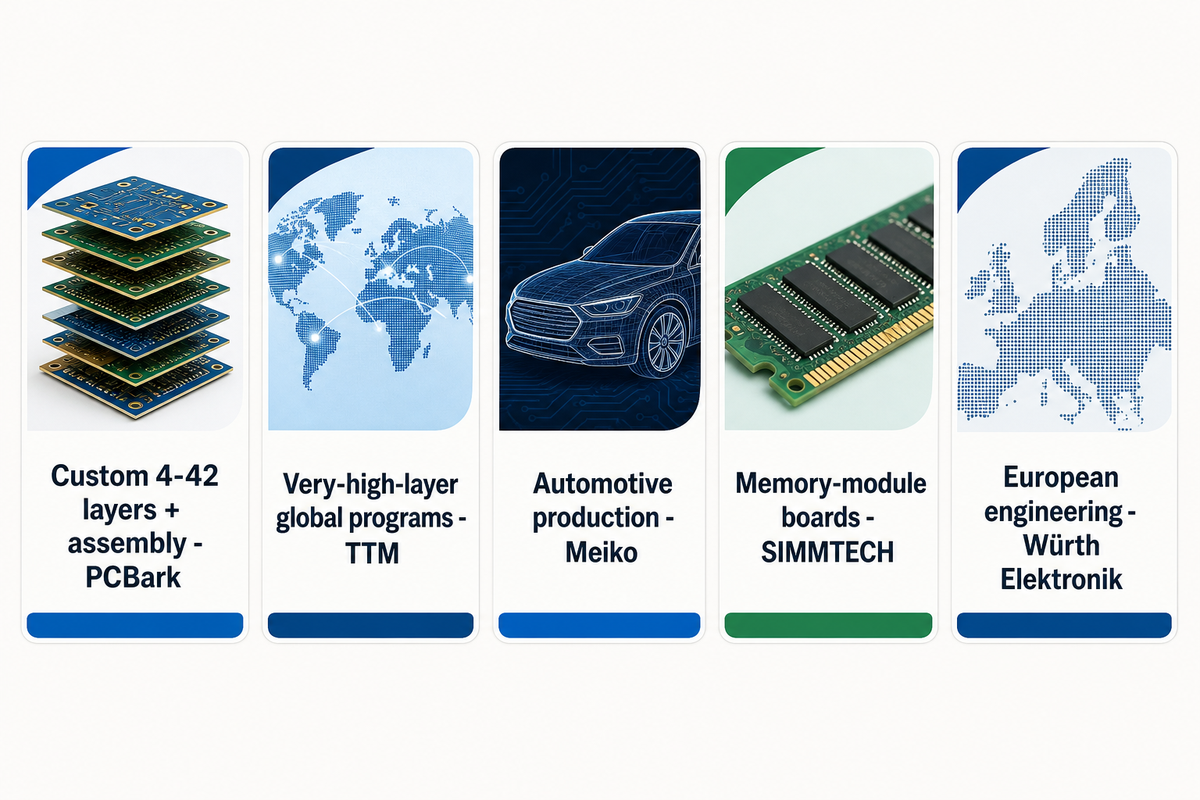
- Best for custom 4–42-layer fabrication with assembly: PCBark
- Best for very-high-layer global programs: TTM Technologies
- Best for automotive multilayer production: Meiko Electronics
- Best for semiconductor memory-module boards: SIMMTECH
- Best for European engineering support: Würth Elektronik Circuit Board Technology
A poor first screen can hide plant-specific limits until after tooling, qualification or transfer costs are committed.
Procurement note: A certificate confirms only its printed scope. It does not replace plant-specific capability review or lot acceptance.
These quick picks are starting points, not a market share ranking. For qualification context, IPC-6012 is the qualification and performance specification for rigid printed boards. For a released stackup, the right factory depends on the laminate system, via structure, impedance plan, end-use standard, annual volume, lot-acceptance method and destination-market restrictions.
How We Selected the 20 Manufacturers
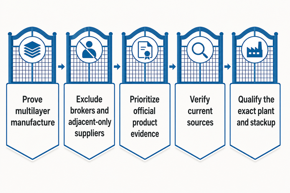
- Manufacturer evidence: every company had to show on a current official page or first-party report that it manufactures multilayer PCBs. A sales office, sourcing company or broker did not qualify.
- Product scope: we excluded marketplaces, directories, media publishers, used-equipment sellers and companies limited to bare laminate, assembly, single-sided boards or other adjacent services.
- Source hierarchy: company facts and product scope came primarily from official company pages, reports and government registries. Standards bodies, government publications, and other technical sources supported the procurement guidance. Google Search was used to discover and cross-check current public pages, not as evidence by itself.
- Verification date: sources were checked on October 5, 2026. Where a suitable public source did not establish a founding year or headquarters, the required wording was “Not publicly disclosed.”
- Comparison rule: a factory’s published layer count or minimum geometry is a screening datum, not a promise for every material, panel size or plant. Buyers should obtain a DFM response and a controlled capability statement for their exact build.
This list is grouped by buyer fit and is not ordered by revenue, output, market share or field performance. First-party product pages confirm that a product line exists, but they remain self-published. An ISO 9001 certificate or RoHS statement also needs scope checking: neither proves that the named fabrication plant, process and product family can meet a released PCB design. For PCB fabrication and related manufacturing services, verify the legal entity, site address and controlled process rather than relying on a group-level badge. The IPC-6012 specification provides the rigid-board qualification and performance context; the purchase specification must still identify the applicable revision, class and site-specific requirements.
Comparison of 20 Multilayer PCB Manufacturers
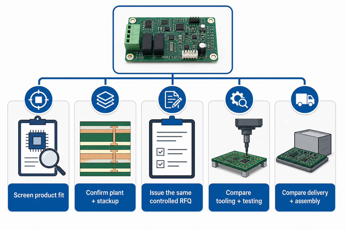
This table can be used as a first screen to generate a short list. Published limits should be read against the IPC-6012 rigid-board qualification and performance framework, then confirmed for the named plant and released stackup. Then the same restricted RFQ should be sent to each listed manufacturer. Once this is done, tooling, test and panel usage should be compared along with certificates, delivery terms and assembly content.
| No. | Company Name | Headquarters | Founded Year | Best For | Brief Introduction | Main Products | Key Advantages | Potential Disadvantages | Official Website |
|---|---|---|---|---|---|---|---|---|---|
| 1 | PCBark | Shenzhen, China | 2010 | Custom 4–42-layer fabrication with turnkey assembly | Custom PCB fabricator and assembly provider. | HDI, multilayer, rigid-flex PCBs; assembly | Published build limits plus assembly and inspection | Smaller field-service footprint than multinational groups | www.pcbark.com |
| 2 | TTM Technologies | Santa Ana, California, USA | 1998 | Very-high-layer global programs | Multi-plant advanced PCB manufacturer. | Multilayer, HDI, RF, flex, rigid-flex | Above-60-layer published capability; global factories | Capabilities and certificates vary by plant | www.ttm.com |
| 3 | AdvancedPCB | Aurora, Colorado, USA | 1977 | US defense and aerospace quick-turn work | US fabricator with several domestic facilities. | Rigid multilayer, HDI, flex, rigid-flex | US factories; 40-plus-layer rigid capability | Limits require facility-specific confirmation | www.advancedpcb.com |
| 4 | AT&S | Leoben, Austria | 1987 | Advanced HDI automotive and industrial programs | Advanced interconnect and substrate manufacturer. | Multilayer, HDI, embedded PCBs, substrates | High-end production in Europe and Asia | No instant prototype pricing path | www.ats.net |
| 5 | Unimicron Technology | Taoyuan, Taiwan | 1990 | High-volume HDI and advanced multilayer programs | Large advanced-interconnect manufacturing group. | Multilayer, HDI, flex, rigid-flex, carriers | Broad portfolio and large production footprint | Few public model-level fabrication limits | www.unimicron.com |
| 6 | Compeq Manufacturing | Taoyuan, Taiwan | 1973 | Computing and communications volume production | Long-running volume PCB producer. | Multilayer, high-layer, HDI, flex, rigid-flex | Multiple PCB technologies at production scale | Limited public lead-time and prototype detail | www.compeq.com.tw |
| 7 | Zhen Ding Technology | Taoyuan, Taiwan | 2006 | Diversified large-scale PCB programs | Multi-technology PCB and substrate group. | Multilayer rigid, HDI, flex, substrates | Large, diversified manufacturing network | Plant and business-unit qualification is essential | www.zdtco.com |
| 8 | Meiko Electronics | Ayase, Kanagawa, Japan | 1975 | Automotive and high-reliability Asian production | Japanese producer with an international factory network. | Multilayer through-hole, HDI, flex, rigid-flex | Automotive focus across several PCB technologies | No public standard lead-time table | www.meiko-elec.com |
| 9 | CMK Corporation | Tokyo, Japan | 1961 | Automotive high-multilayer and HDI boards | Automotive-oriented Japanese PCB manufacturer. | High-multilayer, HDI, build-up, double-sided | Dedicated automotive high-multilayer product family | No public standard pricing or turnaround | www.cmk-corp.com |
| 10 | Tripod Technology | Taoyuan, Taiwan | 1991 | Memory, server and automotive volume boards | Volume producer serving several electronics segments. | Multilayer boards for memory, servers, automotive | Broad application coverage at production scale | Limited public English capability detail | www.tripod-tech.com |
| 11 | Shennan Circuits | Shenzhen, China | 1984 | Telecom and data-center high-layer programs | Integrated PCB, substrate and assembly group. | Multilayer PCBs, substrates, modules, assembly | Several interconnect stages within one group | No standardized small-order quick quote | www.scc.com.cn |
| 12 | Kinwong Electronic | Shenzhen, China | 1993 | Automotive and telecom PCB portfolios | Diversified rigid and flexible PCB producer. | Multilayer, HDI, flex, rigid-flex, metal | Wide technology and material portfolio | Exact limits differ across plants | www.kinwong.com |
| 13 | WUS Printed Circuit | Kaohsiung, Taiwan | 1972 | High-speed server and networking boards | Established high-speed multilayer producer. | Multilayer, HDI, high-speed, automotive PCBs | Long record in networking-board production | No instant prototype quotation workflow | www.wus.com.tw |
| 14 | Victory Giant Technology | Huizhou, China | 2006 | AI, server and graphics high-layer volume | High-precision PCB volume manufacturer. | Multilayer, HDI, flex, rigid-flex | Computing and communications product focus | Limited public prototype-order detail | en.shpcb.com |
| 15 | Suntak Technology | Shenzhen, China | 1995 | Export programs using multiple China factories | Multi-factory Chinese PCB manufacturer. | Multilayer, high-layer, HDI, flex, rigid-flex | Several production bases and product types | Factory allocation needs quotation-stage confirmation | www.suntakpcb.com |
| 16 | KCE Electronics | Bangkok, Thailand | 1982 | Automotive production in Southeast Asia | Automotive-focused multilayer PCB manufacturer. | Multilayer, high-layer and automotive PCBs | Established regional automotive specialization | Narrower portfolio than turnkey electronics groups | www.kce.co.th |
| 17 | SIMMTECH | Cheongju, South Korea | 1987 | Semiconductor memory-module boards | Semiconductor interconnect specialist. | High-layer module PCBs, package substrates | Focused memory and package expertise | Not a general-purpose PCB job shop | eng.simmtech.com |
| 18 | Daeduck Electronics | Ansan, South Korea | 1972 | Network and semiconductor multilayer boards | High-layer network and substrate producer. | Network PCBs, substrates, module boards | Published 20-plus-layer network capability | Concentrated network and semiconductor mix | www.daeduck.com |
| 19 | SCHWEIZER Electronic | Schramberg, Germany | 1849 | European automotive and power custom boards | German automotive and power PCB specialist. | Multilayer, power, RF, embedded, automotive | Documented 18-layer standard range | Standard range ends at 18 layers | www.schweizer.ag |
| 20 | Würth Elektronik Circuit Board Technology | Niedernhall, Germany | 1971 | Prototypes through medium-volume production | German PCB maker with engineering support. | Multilayer, HDI, flex-rigid, RF, thermal | Three German plants; broad technology support | Volume work may use qualified Asian partners | www.we-online.com |
Custom and Global Program Manufacturers
1. PCBark: Best for Custom 4–42-Layer Fabrication with Turnkey Assembly
Disclosure: This guide is published by PCBark. We list ourselves first because this is our website, not because we claim to be the market leader. The other 19 manufacturers are grouped by what they are best for, in no particular order within each group.
PCBark’s current multilayer PCB manufacturing page publishes a 4–42-layer range, a 0.050 mm minimum trace/space at its highest listed tier, impedance tolerance to ±5%, and a maximum board size of 600 × 1,200 mm. The company also offers PCB assembly, inspection and test options, which can reduce handoffs for custom builds. These are self-published screening limits and remain subject to stackup, material, panel and DFM analysis. A practical limitation is a smaller published field-service office network than the largest multinational PCB groups.
2. TTM Technologies: Best for Very-High-Layer Global Programs
TTM publishes conventional multilayer capability above 60 layers and also manufactures HDI, RF and microwave, flex and rigid-flex boards. Its multi-plant footprint is useful when a program needs regional production options or several interconnect technologies under one corporate supplier. However, layer counts, materials, approvals and quality certificates are site-specific; the purchasing contract should name the factory and approved transfer process.
3. AdvancedPCB: Best for US-Made Defense and Aerospace Quick-Turn Work
AdvancedPCB states its Aurora operation isn’t a broker and shows rigid multilayer capability beyond 40 layers. Its US factory network and quick-turn capabilities attract buyers needing domestic rigid PCB fabrication with shorter engineering loops, and controlled Defense and Aerospace sourcing. Capability varies at different locations, so the scope and limitation of certificates should be defined in the RFQ prior to approval.
4. AT&S: Best for Advanced HDI Automotive and Industrial Programs
AT&S identifies multilayer printed circuit boards as a core product. These boards are combined with HDI, embedded-component, and IC-substrate technologies to provide a flexible product offering. Engineered automotive and industrial programs benefit from the company’s product miniaturization, controlled interconnect structures, and product industrialization. It’s expected that quotes be provided for these programs; however, the AT&S website is geared more towards program engagement. For prototype quotes, and estimated lead-times, direct contact with the company is required.
Established East Asian Multilayer Specialists
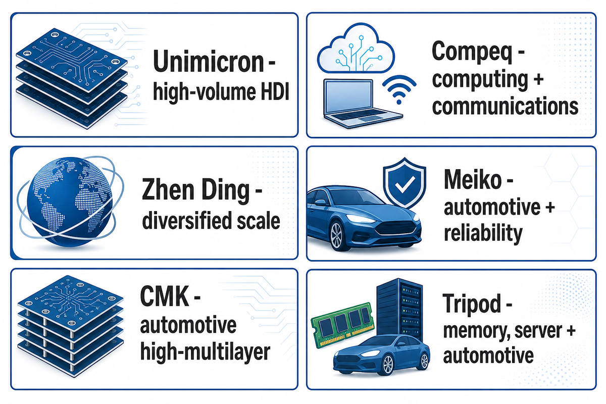
5. Unimicron Technology: Best for High-Volume HDI and Advanced Multilayer Programs
Unimicron group materials cover multilayer, HDI, flex and rigid-flex circuit boards, plus IC-carrier manufacturing. Its scale and broad advanced-interconnect portfolio can suit high-volume computing, communications and electronics programs that need more than one board technology. Public model-level limits are sparse, so buyers should request the assigned plant’s process capability indices, material list, microvia rules and change-control procedure.
6. Compeq Manufacturing: Best for Computing and Communications Volume Production
Compeq offers general information on its multilayer, high-layer count, HDI, flex and rigid-flex technologies. In the computing and communications markets, the company has a large, established production base. Public English materials offer limited standard lead-time and prototype detail. Potential customers should request engineering response time, sample-lot rules and volume ramp ownership in the quotation.
7. Zhen Ding Technology: Best for Diversified Large-Scale PCB Programs
Zhen Ding manufactures PCBs including HDI and multilayer rigid boards as well as flexible circuits and IC substrates. For large customers, the variety can support procurement of many interconnect families from a single provider. In practice, the complexity of its product mix creates an administrative burden: the customer must confirm the legal entity, plant address, approved processes, certificate scope and transfer rules in the quality agreement.
8. Meiko Electronics: Best for Automotive and High-Reliability Asian Production
Meiko’s corporate materials list double-sided, multilayer through-hole, HDI, flex and rigid-flex boards, with production operations serving automotive applications. Its cross-technology factory network is relevant to high-reliability programs that may need rigid and flexible interconnects. For these programs, the public site does not provide an instant quotation or standard lead-time matrix, so supply terms and program support need direct confirmation.
9. CMK Corporation: Best for Automotive High-Multilayer and HDI Boards
CMK provides automotive electronics PCBs and positions its boards for automotive electronics. Buyers considering automotive controllers can consider CMK and other Japanese automotive suppliers. Their reviewed product pages don’t provide standard pricing or turnaround times, and a quote should define samples and deliverables related to PPAP.
10. Tripod Technology: Best for Memory, Server and Automotive Volume Boards
Tripod produces double sided and multilayer PCBs for memory, server, display and automotive applications. Beyond laboratory prototypes, the variety of applications makes it a candidate for production work. Limited public English process detail requires the customer to request the latest stackup rules, loss data and drill limits. Before qualification, the customer should also review the audit package for the specific factory.
China and Southeast Asia Volume Producers
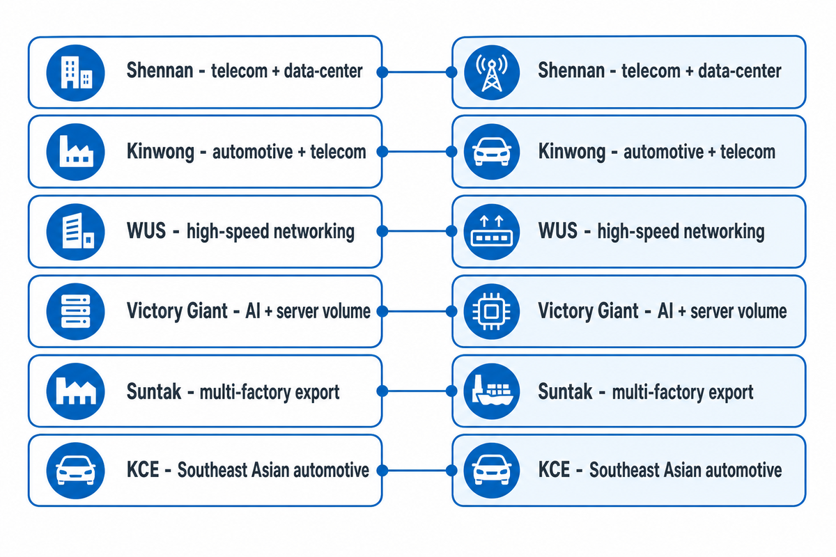
11. Shennan Circuits: Best for Telecom and Data-Center High-Layer Programs
Shennan Circuits makes multilayer PCBs and also has packaging substrate, module and assembly capabilities. These combined capabilities support higher-layer boards and coordination among interconnect stages for telecom and data center customers. Its public site doesn’t provide a standard quick-quote path for small orders. Therefore, low-volume customers should first inquire about their minimum order quantity and level of support for prototypes before design release.
12. Kinwong Electronic: Best for Broad Automotive and Telecom PCB Portfolios
Kinwong lists multilayer, HDI and flexible and rigid-flex boards. The wide range of offerings allows the company to support multiple board construction programs in the same customer’s business (automotive, telecom, etc.). Because the capabilities are distributed among multiple plants, a group capability statement shouldn’t be taken as binding to all the plants. The customer should define the producing site and look for site-bound assurances.
13. WUS Printed Circuit: Best for High-Speed Server and Networking Boards
WUS has produced multilayer boards for decades and presents technology serving high-speed, networking, automotive and HDI applications. It is a logical candidate when signal integrity, low-loss materials and repeatable volume production dominate the sourcing brief. For prototypes, the public site does not expose an instant quotation workflow, so early engagement and complete impedance documentation are important.
14. Victory Giant Technology: Best for AI, Server and Graphics High-Layer Volume
Victory Giant identifies high-precision multilayer, HDI, flexible and rigid-flex boards as core products, with emphasis on computing and communications applications. That product direction aligns with AI servers, graphics hardware and related volume programs. Its public materials emphasize manufacturing scope more than prototype-order mechanics, so buyers should establish sample capacity, engineering ownership and ramp milestones in writing.
15. Suntak Technology: Best for Export Programs Using Multiple China Factories
Suntak outlines a manufacturing network comprising multilayer and high-layer production, as well as HDI and flexible-board technologies. Multiple production bases give options for sourcing of industrial and data-communications programs. Factory allocation is the primary area of due diligence. Capability, certificates, approved materials and any production transfers need to be tied to the factory quoted.
16. KCE Electronics: Best for Automotive Production in Southeast Asia
KCE notes that its plants manufacture advanced, higher-layer-count multilayer boards and has an obvious automotive focus. It’s a suitable Southeast Asian option for automotive electronics buyers sourcing a regionally diversified supplier base. The scope of its business is less broad-based than a full turnkey electronics group. Therefore, buyers requiring assembly and/or unrelated PCBs may need to look elsewhere.
Semiconductor and European Specialists
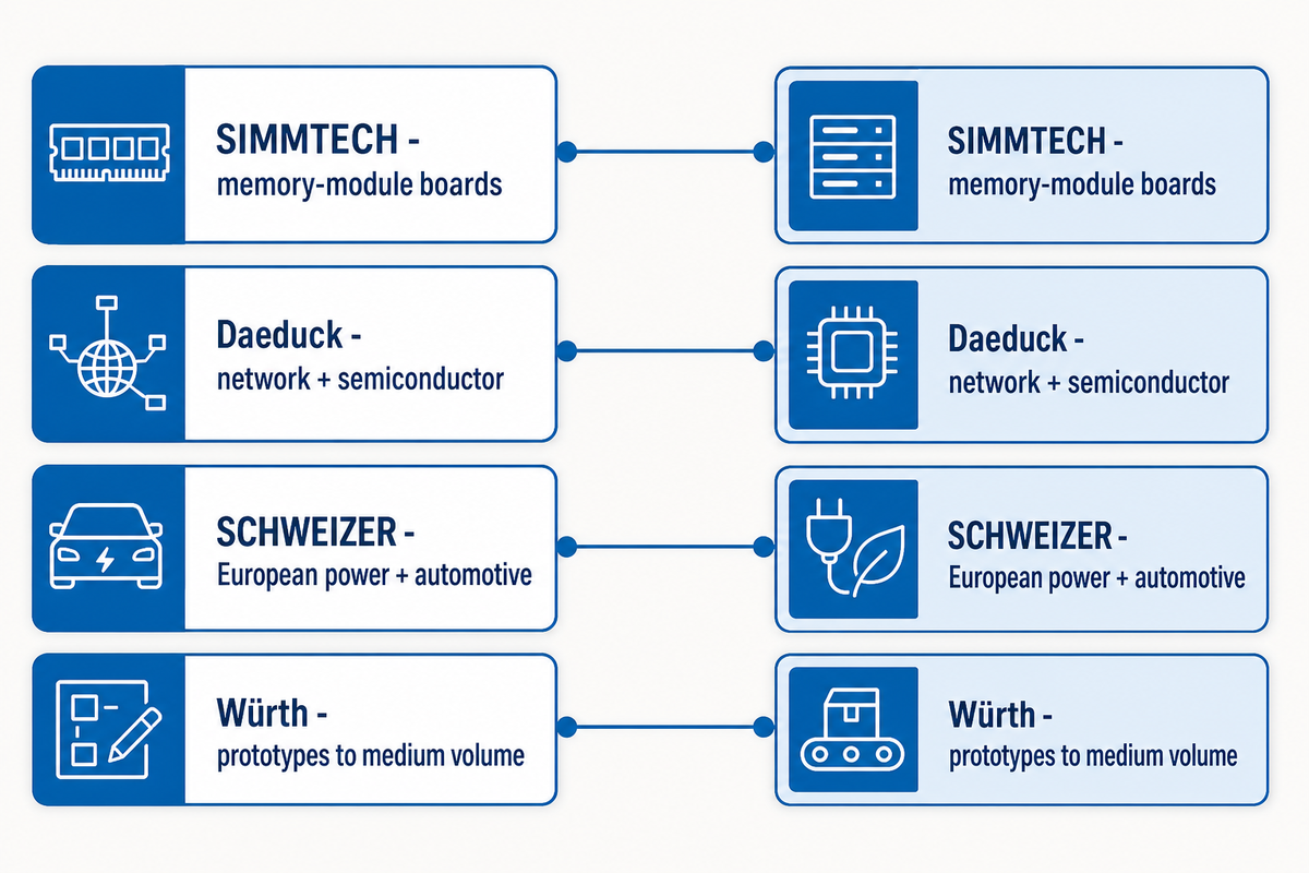
17. SIMMTECH: Best for Semiconductor Memory-Module Multilayer Boards
SIMMTECH states that it has manufactured high-layer PCBs for semiconductors since its establishment and focuses on memory-module boards and package substrates. That concentration is valuable for buyers whose design and qualification needs are closely tied to semiconductor interconnects. It is not positioned as a general-purpose job shop, so ordinary industrial prototypes may fit a broader fabricator more naturally.
18. Daeduck Electronics: Best for Network and Semiconductor Multilayer PCBs
Daeduck’s product materials describe network PCBs with greater than 20 layers, along with semiconductor modules and substrates. This mix is geared toward high-layer interconnects for network and/or semiconductor equipment programs. The scope of the business is focused on these areas; therefore, a team should evaluate fit and support for low volume industrial and unrelated applications.
19. SCHWEIZER Electronic: Best for European Automotive and Power Custom Boards
SCHWEIZER publishes standard multilayer constructions up to 18 layers and 0.6–3.2 mm thickness, alongside power, RF and embedded technologies. The German engineering base is relevant to power electronics and automotive customers requiring custom solutions. The published standard range is limited to 18 layers, and part of its scale strategy may include qualified production partners, thus manufacturing location should be contractually defined.
20. Würth Elektronik Circuit Board Technology: Best for Prototypes Through Medium-Volume Production
Würth Elektronik manufactures basic multilayer, HDI microvia, flex-rigid, RF and thermal management boards. Three German PCB manufacturing plants and an engineering support model position it well to service European prototypes and low volume production builds. Higher volume requirements may use qualified partners in Asia, thus quotation should disclose manufacturing plant, transfer plan and if prototype and production plans are aligned.
How to Choose a Multilayer PCB Manufacturer
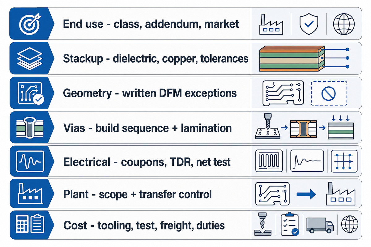
A credible quote begins with a controlled technical package, not only Gerber files and quantity. PCBark’s engineering team sees the same gaps at the handoff between design, fabrication and assembly.
PCB Stackup Design: 7-Point Supplier Fit Check
Perform a seven-field review to link released board requirements with plant evidence prior to any commercial consideration.
| Parameter | Recommended range | Why it matters | How to verify |
|---|---|---|---|
| End-use requirement | Project-defined class, addendum and market | Sets workmanship and eligibility obligations | Name revision, class, addendum, origin and security terms |
| Released stackup | Controlled per part number | Drives thickness, impedance and material selection | Approve dielectric, copper, glass style, finish and tolerances |
| Geometry | Design-specific manufacturable limits | Affects registration, drill yield and annular ring | Request a feature-by-feature DFM exception list |
| Via construction | Documented build sequence | Sequential lamination changes cost and reliability | Confirm via type, aspect ratio, fill and lamination cycles |
| Electrical control | Project-defined impedance and test coverage | Prevents nominal-stackup assumptions | Approve coupons, TDR method and net-test requirements |
| Plant qualification | Named factory and current scope | Group claims may not apply to every site | Check certificate scope, audit status and transfer control |
| Commercial basis | Same Incoterm and acceptance basis | Exposes costs hidden outside unit price | Separate tooling, test, certificates, freight, duties and assembly |
1. Freeze the PCB Design, End-Use and Compliance Basis
State the applicable IPC-6012 revision, performance class and any automotive, medical, aerospace or space addendum. Performance class expresses end-use expectations; it is not a substitute for an application-specific addendum. For regulated programs, also identify country-of-origin restrictions, traceability, cybersecurity and approved-source requirements before quoting. A technically capable plant can still be commercially ineligible.
2. Release a Complete Stackup and Material Definition
Specify finished thickness, copper weights, dielectric thicknesses, resin or glass style where controlled, laminate family, Tg, Dk/Df basis, surface finish and warp/bow requirements. Do not accept a silent material substitution because two laminates share a broad grade. For high-speed work, define the test frequency and method behind the electrical properties, then require written approval for substitutions.
3. Check the Hardest Feature Combination, Not Separate Minima
A combination of minimum trace/space and thicker copper may not be supported by the same build that contains fine lines and a small finished hole. The aspect ratio and board thickness of the greatest dimension may also impact whether a feature can be built. An older AdvancedPCB manufacturer guide uses a nominal 0.020-inch drilled feature with a ±0.003-inch tolerance to explain an acceptable 0.017–0.023-inch interval; this is tolerance-math instruction, not a current universal process limit.
4. Count Lamination Cycles and Define Via Acceptance
Blind, buried, stacked and filled microvias can turn a nominal layer count into a very different manufacturing problem. Request the proposed build sequence, number of sequential laminations, via-fill method, copper-cap requirement and coupon plan. If the design uses stacked microvias, confirm that the quoted factory has qualified that exact structure and material system rather than only a general HDI line.
5. Put Lot Evidence in the Purchase Order
Define what’s included in each lot. Provide net-test results, impedance coupon data, TDR traces if needed, microsection data, evidence of plating thickness, solderability or ionic cleanliness data, certificate of conformance and/or material traceability. Qualification and lot acceptance are separate decisions. A historical audit or certification doesn’t prove a specific shipment met the released drawing.
6. Qualify the Named Plant, Not Only the Corporate Logo
Review the certificate’s address and activity. Confirm CAM, imaging, lamination, drilling, plating, testing and final inspection are performed at the quoted site, or are subcontracted. If production is moved to another site, require advance notice, requalification criteria and sample approval. This is particularly relevant for groups that have many factories or sites in multiple countries.
7. Compare Landed Cost on a Common Yield Basis
The unit price can hide tooling, electrical test, impedance coupons, certificates, panel waste, expedited material, freight, duties, payment cost, assembly attrition and requalification. Panel utilization is especially easy to overlook. In Sierra Circuits’ vendor-authored 18 × 24-inch example, the first layout yields 24 parts at 77.8% utilization and the second yields 16 parts at 52.8%. Sierra states that the 16-part layout costs 33% more than the 24-part layout. That statement is tied to the complete example, not derived from utilization percentage alone, and is not a universal rate.
PCB Fabrication Hidden Cost and Yield Map
A line-item map that exposes where a low unit price can move cost into yield, testing, documentation or supply-chain terms.
| Cost Driver | Where It Hides | RFQ Control | Acceptance Evidence |
|---|---|---|---|
| Panel utilization | Array rails, coupons, spacing and rotation | Request quoted panel and boards per panel | Approved fabrication panel drawing |
| Sequential lamination | Via architecture and buried structures | State the build sequence | Traveler or controlled stackup reference |
| Special laminate | Minimum buy, storage and substitution | Name approved materials and alternates | Lot and material certificate |
| Testing | Flying probe, fixture, TDR and coupons | Separate each test in the quote | Lot-specific test records |
| Quality documents | FAI, PPAP, microsections and reports | List deliverables and frequency | Complete shipment dossier |
| Supply chain | Freight, duties, buffer stock and transfers | Fix Incoterm and approved site | Traceable origin and shipping records |
Multilayer PCB Manufacturing Capability and Cost Data
These publicly available figures help evaluate candidates, but differences in underlying conditions mean they can’t be benchmarked as a single, normative assessment of capability.
| Published Data Point | Value | Source Context | Buyer Use |
|---|---|---|---|
| PCBark layer range | 4–42 layers | Current multilayer product page | Initial layer-count screen |
| PCBark minimum trace/space | 0.050 mm | Highest published tier | Request exact-stackup DFM |
| PCBark impedance tolerance | ±5% | Published capability limit | Define coupon and TDR plan |
| PCBark maximum board size | 600 × 1,200 mm | Published product limit | Confirm with material and stackup |
| TTM layer capability | Above 60 layers | Conventional PCB page | Identify the qualified plant |
| AdvancedPCB rigid capability | Above 40 layers | Aurora facility page | Keep facility named in RFQ |
| AdvancedPCB nominal drill example | 0.020 ±0.003 in | Manufacturer tolerance guide | Check both tolerance limits |
| AdvancedPCB example result | 0.017–0.023 in | Resulting acceptable interval | Verify mating hardware fit |
| SCHWEIZER standard range | Up to 18 layers | Standard multilayer page | Separate standard from custom builds |
| SCHWEIZER thickness range | 0.6–3.2 mm | Standard multilayer page | Check the released finished thickness |
| Daeduck network boards | More than 20 layers | Network product material | Screen high-layer network designs |
| Sierra example panel | 18 × 24 in | Vendor-authored cost example | Ask for the proposed production panel |
| Sierra first array size | 5.125 × 10.925 in | Six arrays, 24 parts | Review array geometry |
| Sierra first part size | 2 × 4.9 in | Four parts per array | Check spacing and rails |
| Sierra second array size | 11.125 × 5.125 in | Four arrays, 16 parts | Review rotation and waste |
| Sierra second part size | 5 × 2 in | Four parts per array | Compare nesting efficiency |
| Sierra utilization comparison | 77.8% versus 52.8% | 24 versus 16 parts per panel | Compare yield assumptions |
| Sierra example cost change | 33% increase | Illustrative panel comparison | Do not treat as a universal rate |
Do
- Issue one controlled data pack and revision.
- Require a written DFM exception list.
- Name the producing plant and approved materials.
- Compare tooling, test and landed cost separately.
Do not
- Compare quotes built from different stackups.
- Treat a logo-level certificate as plant proof.
- Assume catalog minima combine on one board.
- Approve substitutions through informal email only.
Frequently Asked Questions
Which Is the Best Multilayer PCB Manufacturer for High-Layer-Count Boards?
TTM is a strong starting point for very-high-layer programs because it publishes capability above 60 layers. PCBark publishes a 4–42-layer range, AdvancedPCB’s Aurora page states above 40 layers, and SCHWEIZER’s standard multilayer range reaches 18 layers. SCHWEIZER’s standard multilayer capability is 18 layers. These are screening figures, not comparable promises. Material, thickness, copper, holes, lamination cycles, panel size, plant and certification can lower the feasible count. To get a true plant-bound estimate, provide the released stack-up to the prospective supplier.
Who Is the Largest Multilayer PCB Manufacturer in the World?
There is no single defensible answer without defining the metric and period. Revenue, PCB-only sales, multilayer output, panel area and group size can produce different leaders. For procurement, plant eligibility, process capability, available capacity and lot performance matter more than unsupported size claims.
Are Chinese Multilayer PCB Manufacturers Reliable?
Yes, qualified Chinese factories can be reliable, but country alone does not establish performance. Audit the named plant, confirm certificate scope, run a sample build and put lot evidence in the order. Review on-time and corrective-action records, verify approved materials, control production transfers, require traceable substitutions before volume release, and document accepted deviations in the quality agreement and shipment records. Defense or other regulated programs may impose origin, traceability, trusted-supplier or cybersecurity rules that make an otherwise capable factory ineligible.
How Much Does a Multilayer PCB Cost?
No responsible universal price range is available from current public evidence. Layer count, panel use, laminate, holes, via sequence, finish, testing, quantity, lead time and delivery terms all change the quote. Send every factory the same released stackup and acceptance package.
What Is the Difference Between a Multilayer PCB Manufacturer and a Supplier?
A board manufacturer produces the board, while a supplier may manufacture, broker, or arrange for production by someone else. A supplier may still add value through engineering, assembly, and logistics, but the buyer must identify who’s in control of CAM, lamination, drilling, plating and testing. Ask for the name of the producing factory, subcontracted processes, and change-notification. Reliance on the seller’s brand shouldn’t be assumed.
What Should I Measure During First-Article Acceptance?
Verify the critical dimensions of the drawing and check the electrical and material records as specified. Other things that may be verified are the finished thickness, hole diameter, annular ring, registration, copper and plating thickness by cross section, impedance coupons, continuity and isolation, solder mask registration, surface finish, bow and twist. The sampling plan and acceptance criteria should be aligned to the standard, class and application released.
Build a Shortlist Around the Released Board
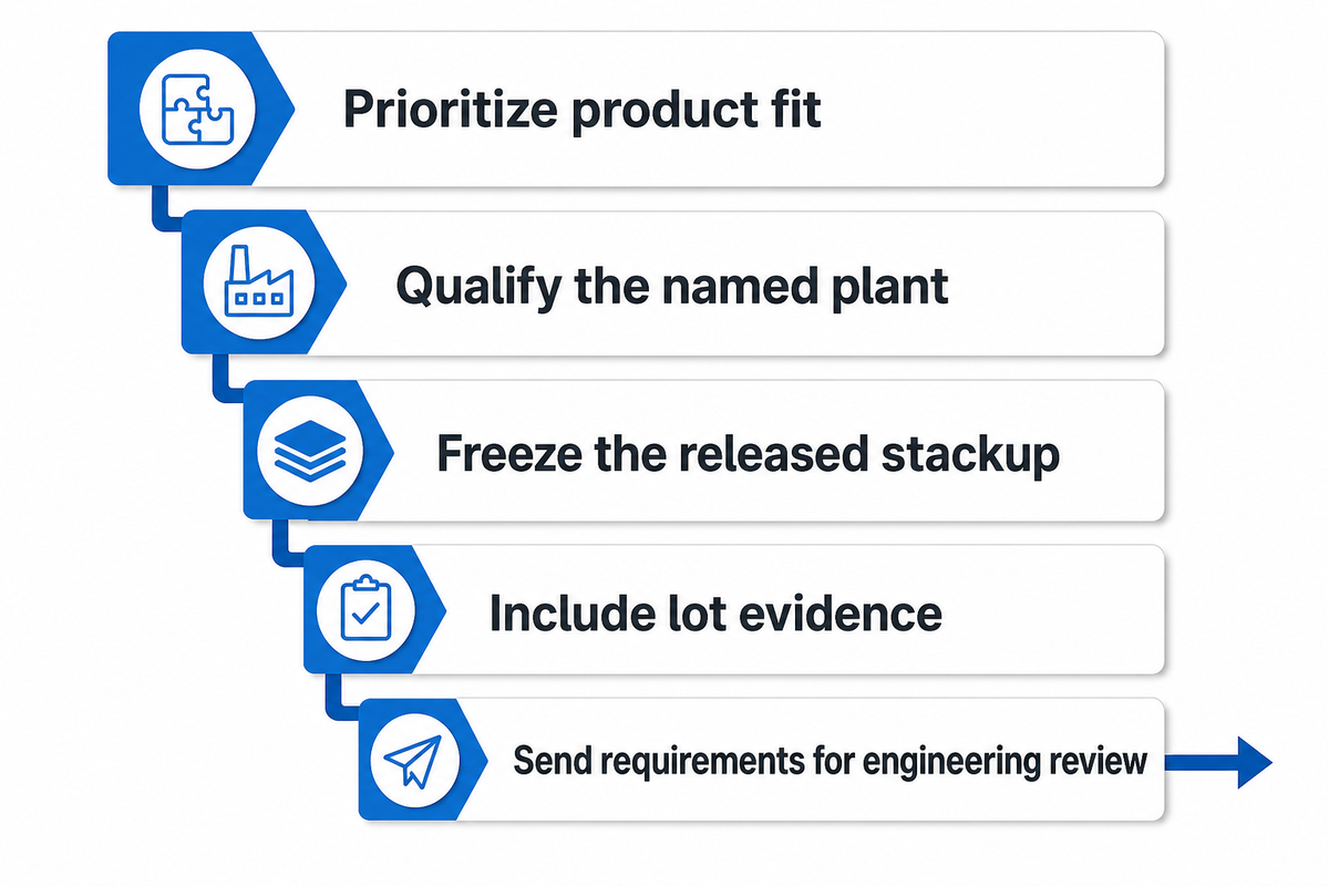
The 20 companies above cover custom builds, large aerospace and other complex programs, automotive electronics, high-speed networking, semiconductor interconnects and European engineering support. A reasonable first step still requires a controlled technical package and a response from a producing plant. If your project needs 4-42 layers with fabrication and assembly coordination, review PCBark’s multilayer PCB capabilities, HDI PCB options and inspection methods, then send the stackup and acceptance requirements for engineering review.
Prioritize product fit, qualify the named plant, freeze the stackup, and include lot evidence in your order. Published capability is the opening question, not the acceptance result.
References & Sources
- IPC-6012F table of contents – Qualification and Performance Specification for Rigid PCBs.
- IPC-1791 table of contents – Trusted Designer, Fabricator and Assembler Programs.
- US Department of Defense Federal Register notice, July 2, 2026 – Public statement on Covered PCB sourcing and concerns related to supply chain security.
- NASA GSFC-STD-8001 – Requirements for Printed Wiring Boards for NASA’s Space Programs.
- EE Times report on a named QML site audit – An example of qualification to a specific facility.
- WIPO patent publication WO2025029814A1 – a 2025 public record concerning multilayer printed circuit board manufacturing equipment.