Get in touch with PCBark Company

When FR-4 Can’t Take the Heat: Why Engineers Move to Ceramic PCB
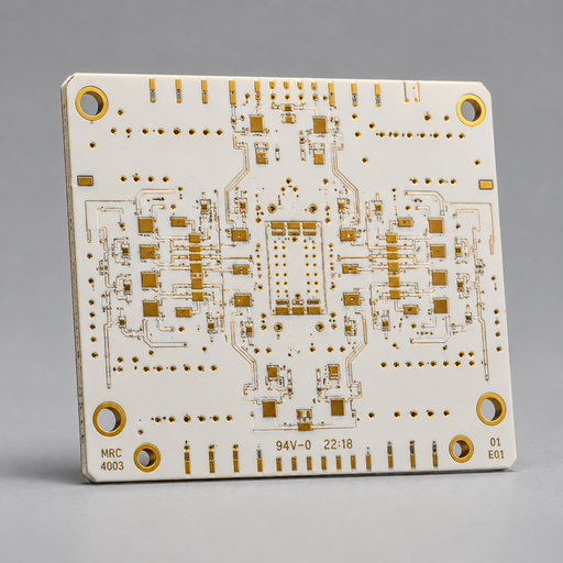
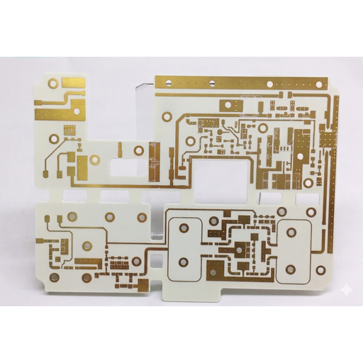
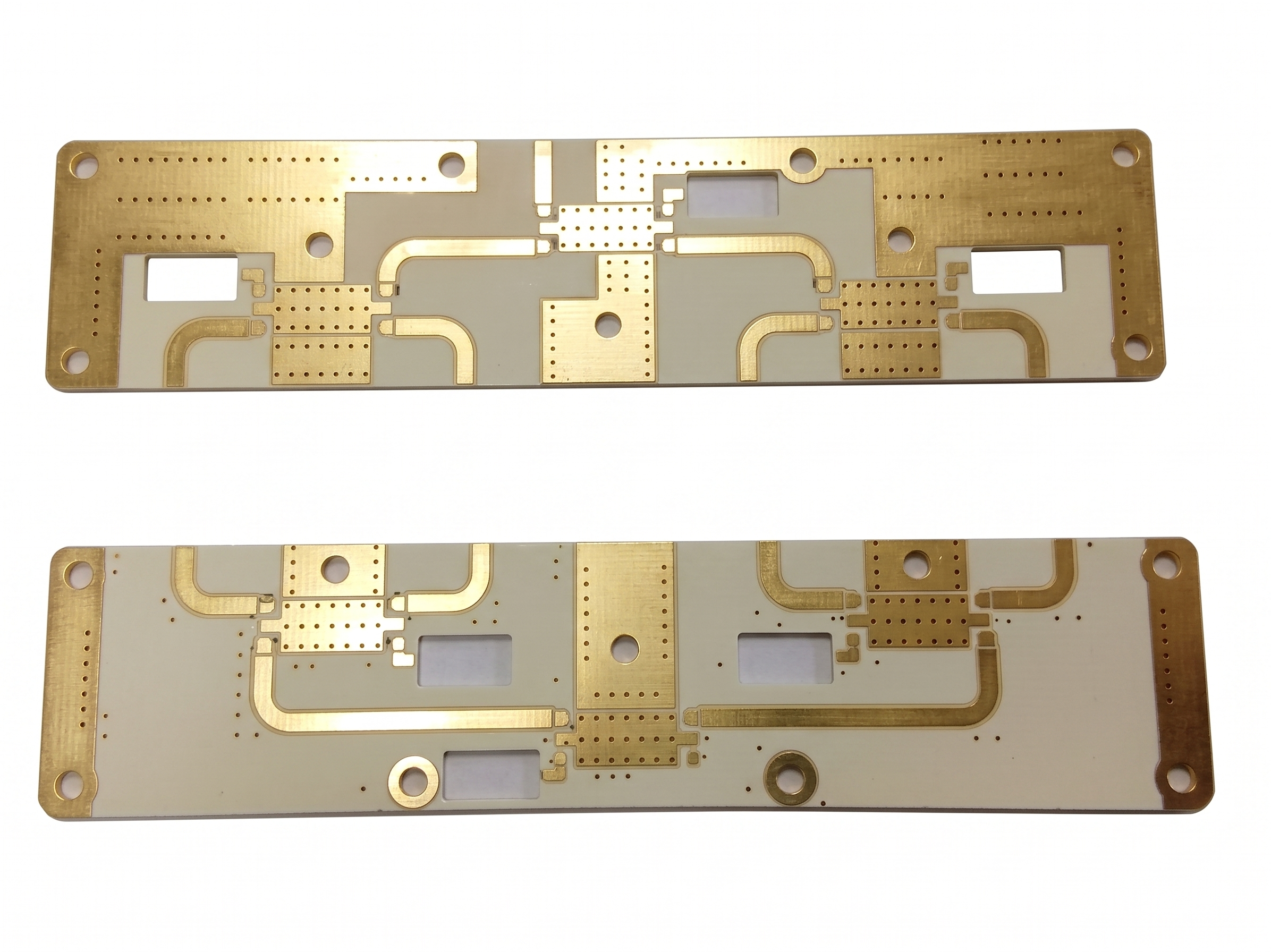
A ceramic PCB is a printed circuit board in which the standard board’s glass-epoxy FR4 laminate is replaced with an alumina (aluminum oxide, Al2O3), aluminum nitride, silicon nitride, or beryllium oxide substrate, with copper bonded directly to the ceramic so heat dissipation happens at the junction rather than cooking it. That combination of high thermal conductivity with strong electrical insulation is exactly why design teams switch for serious thermal management. Where FR4 runs around 0.3 to 0.5 W/m·K, even the least expensive ceramics reach 24 to 30 W/m·K, about twenty times faster, and aluminum nitride goes much higher, to 170 W/m·K and above.
The Honest Version:
ceramic isn’t the answer for every board. If your design runs cool and ships in consumer volumes, FR-4’s cost and design flexibility usually win. Ceramic earns its place when heat, voltage isolation, frequency, or harsh-environment reliability are the constraint — and that’s exactly the work this page is about. With 16+ years and 500,000 m²/yr of EMS capacity, PCBark builds both sides of that decision in-house, so the recommendation you get is honest rather than a sales reflex.
Technical Reference:
metal-ceramic composite heat-path structures, Google Patents WO2025114526A1.
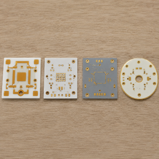
Ceramic PCB Materials: Alumina Vs. Aluminum Nitride Vs. Si₃N₄ Vs. BeO
Here’s the counter-intuitive part most spec sheets skip: the highest thermal conductivity isn’t automatically the best choice.
Aluminum nitride transfers heat five-to-seven times faster than alumina, yet alumina DBC substrates tolerate nearly twice as many thermal cycles as AlN DBC, AlN is more brittle and isn’t always compatible with conventional metal pastes without custom matching, and silicon nitride, with lower conductivity than AlN, is what the automotive industry trusts for IGBT modules because its fracture toughness handle vibration. Choosing a ceramic substrate is a balancing act between heat transfer, thermal-cycle durability, dielectric performance, and cost.
The following table compares property data that our engineers would use for DFM with the application each material is found to win in reality. Use it to order a shortlist of a substrate before requesting a quote.
Ceramic Substrate Selection Matrix (Al2O3, AlN, Si3N4, BeO) — Material Properties Vs. Application Fit
| Substrate | Thermal Conductivity | Dielectric Constant (1 MHz) | CTE (ppm/K) | Best-Fit Application |
|---|---|---|---|---|
| Alumina (Al₂O₃, 96–99%) | 24–30 W/m·K | 9.4–10 | 6–7.5 | General LED, signal & control boards, cost-sensitive thermal work |
| Aluminum Nitride (AlN) | 170–320 W/m·K | ~9 | 4.6 | High-power LED, laser modules, dense power electronics |
| Silicon Nitride (Si₃N₄) | 80–90 W/m·K | — | 2.5 | Automotive & aerospace IGBT — best fracture toughness under vibration |
| Beryllium Oxide (BeO) | 184–300 W/m·K | ~6.8 | — | Extreme thermal duty (handling restrictions apply) |
The Ceramic Material Thermal Conductivity Ladder
Think of substrate selection as climbing a heat-transfer ladder — Al2O3 alumina at 24–30 W/m·K for everyday LED and a ceramic PCB prototype, up to AlN at 170–200 W/m·K for dense power work, and our maximum-capability builds at 250 W/m·K or above. Unlike most ceramic PCB suppliers who push the highest number, we size you to the rung your thermal budget and cost actually need — because over-climbing the ladder just adds cost you don’t recover.
There are two figures worth talking about. First up, Dk – an RF engineer on r/rfelectronics pointed out that alumina Dk ranges from 9.4 to 9.9 across different databases and vendors – this difference is a real, purity dependant effect, which explains why we report 9.4 for 96% alumina and 10 for 99% rather than some one-number marketing spiel. Second, CTE – the silicon chip expands at around 2.6 ppm/K so AlN (4.6) and Si₃N₄ (2.5) are close enough to the chip that the strain relief at the interface doesn’t kill the power module.
Process reference: DCB process for aluminum nitride substrates, Google Patents CN104105678A.
SYS.01 // METALLIZATION_TECH
Metallization Technologies: Thick Film, Thin Film, DPC, DBC, AMB & LTCC/HTCC
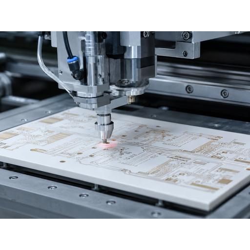
The substrate dictates heat egress; the metallization determines the current density supported by copper and the definition capability of the traces. When the wrong process is applied, a good ceramic is paired with a conductor that can neither support the necessary traces nor survive the bonding process. PCBark operates a complete range of processes internally to ensure the metallization selected is a suitable mate for the ceramic substrate and current density – rather than a capability constraint of a single product line.
Ceramic PCB Metallization Processes — What Each One Is For
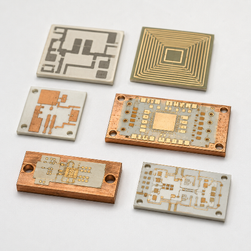
Operating temperatures aren’t mere details; they’re enablers of product reliability. The high-temperature eutectic bond used with DBC substrates, provides high copper density which is essential for 400-1200V electric vehicle inverter applications. In contrast, the lower-temperature bond of AMB is essential to braze copper directly to silicon nitride, which is why it’s the method specified for all traction-grade module types. As Active Metal Brazing is one of the newest of these technologies, continuous research and patented applications such as US20240178098A1 for the metal ceramic PCBA production, and CN113953612A document further developments.
By integrating DPC, thick film, DBC and AMB technologies on a single site, we’re able to match the ceramic base to the required current density for a DBC ceramic PCB, instead of steering customers toward what a single product line can accommodate, the trap that frequently results in boards being over-specified or under-engineered.
Ceramic PCB Vs. FR-4: Performance And Cost, In Numbers
Typically the comparison of ceramic vs. FR-4 centers on the higher individual piece price of ceramic. But this comparison only considers price in a vacuum; ceramic is still the less expensive choice at the system level when compared to the de-ratings and external heat sinks required by a high-power circuit board.
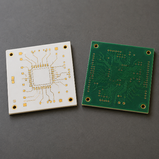
| Property | Ceramic PCB | FR-4 PCB |
|---|---|---|
| Thermal conductivity | 24–170+ W/m·K | 0.3–0.5 W/m·K |
| Max. operating temperature | 150–250 °C (350 °C+ on max-tier builds) | ~130 °C (Tg) |
| Thermal-cycle endurance | Superior — low CTE, fewer solder-joint failures | Limited |
| RF / high-frequency loss | Low dielectric loss, stable | Higher loss |
| Board-level cost | Higher | Low (≈$1–10 / sq ft) |
| Best fit | High-power, high-temp, RF, harsh environments | General-purpose, cost-driven volume electronics |
Total-Cost-Of-Ownership View
We can’t provide a percent ROI because it varies with your power level and cost of failure – and made up numbers on a website don’t serve any purpose. What we know from the field is this: high temp circuits typically offset the higher initial price of ceramic through lower thermal-related failures, elimination of a secondary heat sink, and more possible power per area. Our customers that make LEDs report ceramic as an increase in their product lifespan of ~30% over FR4. We can use our TCO calculator and team of engineers to evaluate your product duty cycle and board design.
Technical reference: ceramic circuit board with bonded metal plate, Google Patents WO2013002407A1.
Ceramic PCB Applications: LED, Power Modules, Automotive, RF, IGBT & Aerospace
Ceramic PCBs tend to go where PCB failure costs or risk are high, including but not limited to military/defense, Aerospace, medical devices, automotive electronics, high-power lighting (LED), high-power supplies and power module sub-strates. The demands of such an application not only influence material selection, but it often dictates the allowable metals and minimum testing needed which drives our unique application-driven product line approach.
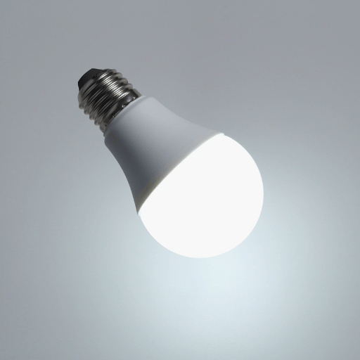
High-Power & UV-C LED
High-Power & UV-C LED
Alumina and AlN substrates pull heat from the junction so high-brightness and UV-C arrays hold output and lifespan. Pairs with thick-film or DPC.
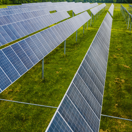
Power Modules & IGBT
Power Modules & IGBT
EV/HEV inverters at 400–1200 V need DBC (Al₂O₃/AlN) or AMB (Si₃N₄) for heavy copper and high isolation.
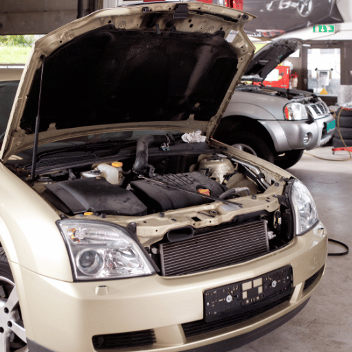
Automotive Electronics
Automotive Electronics
Si₃N₄ AMB resists the vibration and thermal cycling under the hood; low CTE protects the silicon interface.
RF & Microwave
RF & Microwave
Low dielectric loss and dimensional stability keep signal integrity in amplifiers and antennas. Thin film for fine geometry.

Aerospace & Defense
Aerospace & Defense
High-temperature stability and reliability for avionics, satellite, and guidance electronics where failure isn’t an option.
Lasers & Semiconductor
Lasers & Semiconductor Packaging
AlN submounts and ceramic package substrates manage heat in laser diodes and chip-scale packages.
Where many ceramic PCB suppliers stop at the bare board, PCBark carries each of these applications through to a populated, tested assembly on one line, so a 250 W/m·K AlN power-module substrate and its mounted devices are qualified together, not handed between two vendors. That single-source path is what keeps a high-reliability build from failing at the interface no one owned.
Process reference: active metal brazing (AMB) copper-clad ceramic substrate for power modules, Google Patents CN113953612A.
What Drives Your Ceramic PCB Price
Rather than a sticker price, these elements truly dictate what drives ceramic PCB quoting. Make these clear on your RFQ for an accurate number:
01
Substrate & Tier: 96% alumina isn’t the same price point as AlN or Si₃N₄.
02
Metallization: Thick film, DPC, DBC, and AMB are different sets of process steps, and different prices.
03
Layer Count And Geometry: Multilayer adds steps, and fine traces (e.g. 0.05 mm) make fabrication complex.
04
Copper Thickness And Surface Finish: Heavy copper needs more etch time; precious-metal plating (NiPdAu, ENEPIG) adds cost.
05
Volume And Scope: Prototype vs. production, bare board vs. full assembly.
Give us your substrate, metallization, and volume and we’ll return a firm quotation and lead time for your build.
Submit Your RFQ →Procurement Guide: From Prototype To Volume, On One Turnkey Line
Two significant frustrations surface often for real buyers and users. First, on sites like reddit’s /r/AskElectronics, users ask where to find readily available “ceramic (alumina) PCB substrate” from suppliers that don’t require thousands of dollars of NRE per design, especially one with a “clear ordering process,” while others are looking for Asia-based vendors that hold low-CTE material to spec. This has been a perennial frustration among designers seeking cost-effective ceramic solutions. Second, as previously touched on, procurement desks constantly find themselves in situations where a 15-day quoted build lead time can mean 15 days from actual production commencement, after which some customers discover an additional “assembly lead time.” For many overseas sourced orders that we fill, and particularly in China, the real deciding factors are delivery lead time, flexible minimum order quantities (MOQ), and final landed cost; and so we always try to make these terms absolutely clear in advance, in an effort to remove any of these costly, business-disrupting issues.
One Integrated Source Of Supply – From Concept To Reality!
As a certified EMS partner, PCBark doesn’t only produce bare ceramic PCB boards, but can also take care of your design through to final product. Our integrated service means your PCB assembly moves through the design process, component sourcing, ceramic PCB manufacturing, assembly, all and the test stages – all performed under one roof – so your final Ceramic PCB Assembly and their substrates are tested and fully qualified together.
Interactive Ceramic PCB Engineering Tools
MOD-01
Ceramic PCB Substrate Selector
Answer three questions to shortlist the right ceramic substrate — alumina, aluminum nitride, silicon nitride, or BeO — before you request a quote from PCBark.
Launch Selector →MOD-02
Ceramic PCB Vs. FR-4 Thermal Headroom Estimator
A first-order comparison of how much hotter an FR-4 board runs versus a ceramic substrate for the same heat load. Directional only — PCBark models your real stack-up during DFM.
Calculate Headroom →MOD-03
PCBark Ceramic PCB Capability-Tier Matcher
Map your toughest requirement to PCBark’s Standard / Best / Maximum capability tier — so your RFQ lands in the right place and skips a clarification cycle.
Match Tier → DATABASE.FAQ // SYSTEM_Q&A
FAQ: Ceramic PCB Questions Answered
Where can I find a ceramic PCB supplier that can actually build my design?
You’re describing a common frustration, buyers often struggle to find an accessible ceramic PCB source with a clear path from quote to order. PCBark handles alumina, AlN, Si₃N₄, and BeO substrates across thick film, DPC, DBC, and AMB, from 5 × 5 mm prototypes to volume production, and assembles the populated board on the same line. Send your substrate, metallization, and volume to get a quote.
Alumina or aluminum nitride — which ceramic PCB should I choose?
Choose alumina (24–30 W/m·K) for general LED, signal, and cost-sensitive thermal boards. Choose aluminum nitride (170–320 W/m·K) when heat density is the constraint, high-power LED, lasers, dense power electronics. For automotive or aerospace IGBT modules under vibration, silicon nitride with AMB is often the better answer despite lower conductivity, because its fracture toughness survives thermal cycling. Our engineers confirm the call during DFM.
Is a ceramic PCB worth the higher price over FR-4?
At the board level, ceramic costs more than FR-4 (which runs about $1–10 per square foot). The justification is system-level: FR-4 conducts ~0.3–0.5 W/m·K and tops out near 130 °C, so a high-power design pays for heatsinks, derating, and earlier field failures. When heat, voltage isolation, or harsh-environment reliability is the real constraint, ceramic’s lifetime cost is typically lower. If your board runs cool in consumer volumes, FR-4 is the smarter choice.
What is the dielectric constant of alumina ceramic PCB?
About 9.4 for 96% alumina and 10 for 99% alumina at 1 MHz; aluminum nitride sits near 9. Published figures vary slightly (9.4–9.9) with purity and test frequency, so we specify the value for the grade you order rather than a single number.
What’s the difference between DBC and AMB ceramic substrates?
DBC (Direct Bonded Copper) eutectically bonds copper to alumina or AlN at about 1065 °C and is the workhorse for high-current power modules. AMB (Active Metal Brazing) joins copper at about 800 °C and is the practical route for silicon nitride, delivering the highest reliability for automotive and traction IGBT modules.
What is the most expensive type of PCB?
Among ceramic options, beryllium oxide and high-layer-count co-fired (HTCC) packages sit at the top, followed by AMB silicon nitride and multilayer AlN. Cost tracks material, metallization complexity, layer count, and qualification effort, which is why matching your requirement to the right capability tier, rather than over-specifying, controls the price.