Get in touch with PCBark Company

Top 20 PCB Manufacturers in the World

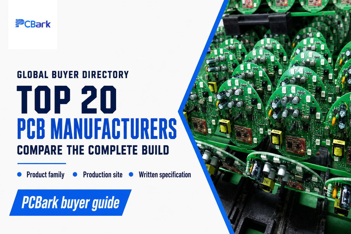
An unranked editorial shortlist for PCB buyers
The board you require determines which PCB manufacturers to pick first. PCB manufacturers are companies that provide printed circuit board manufacturing services, producing the bare boards specified by a customer’s design. A factory for a standard prototype may demand a different process for fine-pitch HDI, heavy copper or rigid-flex. This article compares twenty suppliers based on the published scope of fabrication and the issues buyers should resolve before ordering.
Editorial note: PCBark publishes this article and appears first by editorial request. The other companies are presented in no particular order. “Top” describes this editorial selection; it doesn’t mean the twenty largest manufacturers or an independently verified ranking of quality, market share or technical performance. QueenEMS is included with one disclosed link as part of a reciprocal link exchange. That relationship isn’t evidence of superior manufacturing capability.
The criteria published show publicly available bare-board fabrication and an identifiable sales channel for PCB products. The mix includes major manufacturing groups, specialty fabricators and online prototype services. The published information for the companies was reviewed in September 2026. The published specifications should be reviewed as supplier statements, and the accepted quote and fabrication drawing should define the intended build.
How to use this PCB manufacturer comparison
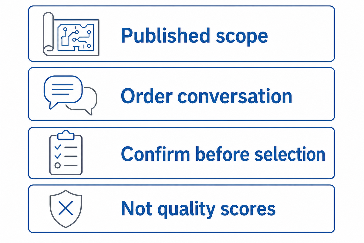
Beginning your shortlist of PCB manufacturers is done by matching the board family, production routes and engineering support and then comparing costs. The table below lists published offerings with no quality scores assigned. Headquarters, sales offices and factories can be in varied countries so ask which legal entity will accept the order and which site will manufacture it.
The first contact Factory-and-Order Scope Table prompts sensible questions that don’t involve confirmed minimum order or availability promises. Website menus show product families, but not that all listed processes can be combined in every factory. Begin with the given product family, and then request a factory-specific capability statement.
The list of PCB manufacturers has some regional segregation. AT&S or Würth Elektronik, as well as Eurocircuits or Unimicron Germany, can be options for buyers of PCB manufacturers within Europe. When sourcing a PCB manufacturer online, ensure that the indicated quote includes the required testing and that the configurator allows the complete construction. Geography and ordering convenience are filters, not quality assessments.
| Company | Published manufacturing scope | Order conversation | Confirm before selection |
|---|---|---|---|
| PCBark | Rigid, multilayer, HDI, flex and thermal boards; assembly | Fabrication with engineering review and optional assembly | Build site and conflicting fine-line limits |
| TTM Technologies | Multisite PCB, substrate, RF and advanced interconnect products | Technology and program requirements | Qualified factory and manufacturing route |
| AT&S | High-end PCBs and IC substrates at different sites | PCB versus packaging-substrate program | Product-specific site and process |
| Zhen Ding | FPC, HDI, SLP, rigid, rigid-flex and substrates | Product-family and production-program fit | Correct business unit and available capacity |
| Unimicron | PCB and IC-substrate group; separate German PCB operation | Regional manufacturing and product route | Parent, subsidiary and origin documentation |
| Compeq | Multilayer, HDI, high-layer-count, flexible and rigid-flex | Construction and production needs | Current site-specific technology statement |
| Tripod Technology | Double-sided and multilayer PCBs | Released production capability | Production versus development targets |
| Meiko Electronics | Multilayer, HDI, flex, rigid-flex and thermal products | PCB production and any separate assembly scope | Manufacturing entity and test package |
| Kinwong | Rigid, flexible, metal-base, HDI and specialist boards | Application-specific construction | Factory, laminate and process combination |
| Shennan Circuits | PCBs, packaging substrates and electronic assembly | Select the relevant business division | Bare-board versus substrate specifications |
| WUS Taiwan | HDI, any-layer HDI and high-speed constructions | Via architecture and signal requirements | Entity, approved stack-up and qualification |
| Nan Ya PCB | Conventional, HDI, rigid-flex and packaging substrates | Board versus IC-substrate program | Manufacturing site and technology family |
| Würth Elektronik CBT | German PCB plants and qualified Asian partner routes | Prototype-to-series sourcing route | Actual production origin and responsibility |
| Eurocircuits | European prototype and small-series PCB/assembly | Digital checks and service-class fit | Selected technology class and assembly scope |
| Sierra Circuits | US fabrication and assembly with service-specific limits | Standard versus advanced package | Package limits and included test documentation |
| AdvancedPCB | US facilities with different technology specialties | Match construction to a named facility | Factory capability and certificate scope |
| Summit Interconnect | North American advanced PCB manufacturing network | Program and facility qualification | Site-specific process and delivery commitment |
| JLCPCB | Online rigid, flex, metal-core and assembly services | Configurator-supported construction | Board-family restrictions and via options |
| PCBWay | Standard and advanced fabrication; assembly | Standard online order versus engineering route | Construction-specific limits and plant |
| QueenEMS | Bare-board fabrication with optional assembly | Written confirmation of complete construction | Layer-range conflict and contracting entity |
For the underlying process rather than a supplier list, use the PCBark fabrication service overview. When comparing assembly, keep in mind that the placement work and the components are separate from the bare-board quote. A PCB fabrication manufacturer may also offer assembly services, but this doesn’t imply that both operations are located at one facility.
1. PCBark
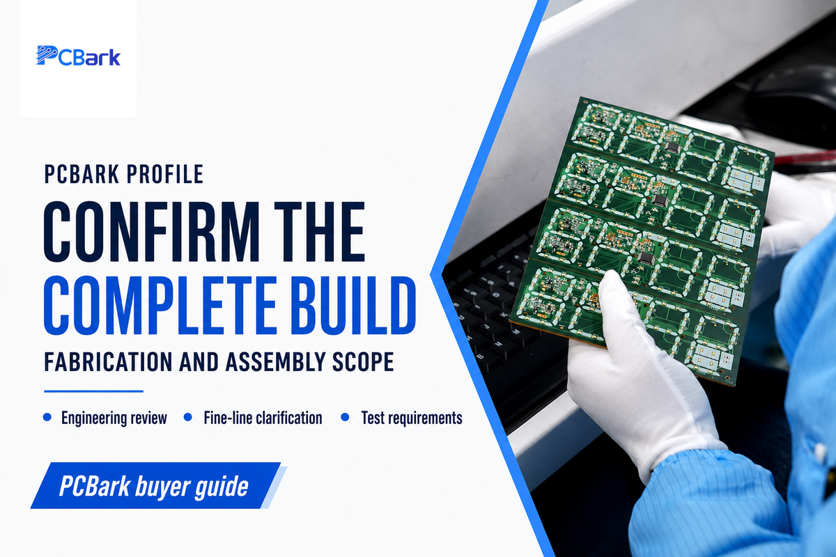
PCBark publishes bare-board fabrication and PCB assembly services for those seeking engineering review together with the production process. Their stated coverage would include rigid multilayer, HDI, and flexible and thermal PCBs. Start with the complete manufacturing dataset; the fine-line numbers on the website differ between pages and clarification is needed to answer the request.
Established and location: The published history of PCBark starts in 2010. The company traces a history to a Shenzhen factory as well as moves to Huizhou and Jiangxi branch. These events don’t determine one single corporate address. Make sure you confirm the address of production and contracting on the quote.
Enterprise and products: The company describes an integrated fabrication and assembly model. A number of published documents show FR-4, high-Tg, FR-4, aluminum, copper core, Rogers, and a number of ceramic options. All of these options belong to different board constructions. The capability matrix shows 1-42 layers, which doesn’t mean that all of these materials support the entire range.
Process limits and finishes: One manufacturing page says 3/3 mil trace/space, while the capabilities page says 4/4 mil. Ask engineering which limit is relevant to the copper weight and stack-up. From these pages, no single mechanical-drill or laser-via minimum was established. Listed finishes are lead-free HASL, OSP, ENIG, immersion silver, and immersion tin.
Applications and quality: The scope of products covers routine electronics and more advanced thermal or dense interconnect designs. PCBark cites AOI, flying-probe, X-ray and in-circuit testing in services; assembly inspection shouldn’t equate to bare board testing. Supplier-hosted certification images require the current issuer, factory, and scope check.
Buying Advantage and Caveat: fabrication and assembly can be addressed via one engineering channel. Address the 3/3 vs 4/4 mil discrepancy prior to approving a fine line order, and specify the test output. The published manufacturing capability matrix can be a starting point for negotiations.
Official website: https://pcbark.com/
Any implementation of the quoted fine-line rule in contrast to released artwork may require a layout modification after order placement. Account for this risk before setting a delivery date.
2. TTM Technologies
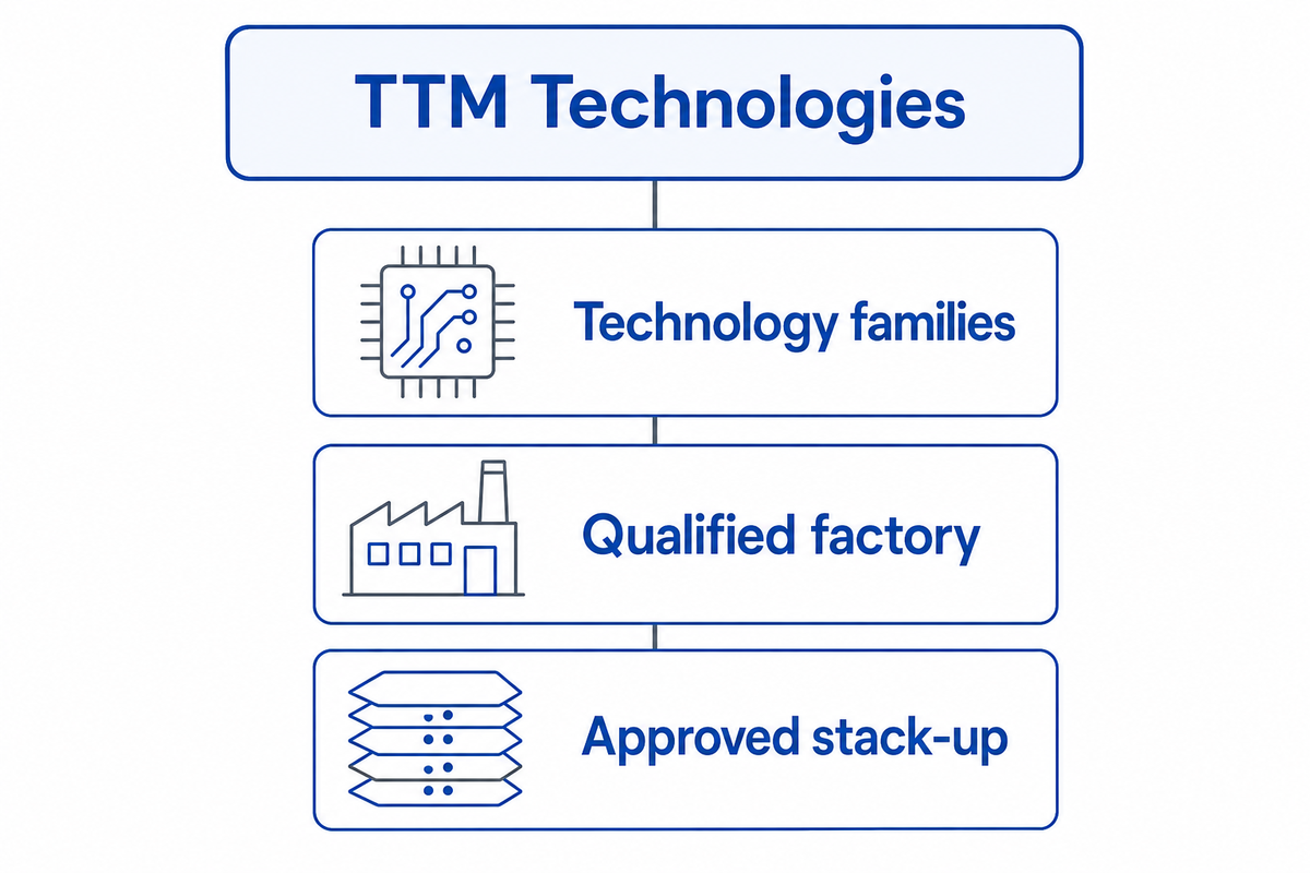
TTM Technologies is an international PCB and substrate manufacturer with various manufacturing paths. TTM’s published catalog includes standard boards, HDI, flex and rigid-flex, RF and microwave products, and thermal solutions. Customers need to define the technology and provide a program overview in order to assess the proposed factory against the actual board build.
Established and headquarters: TTM’s corporate filings identify 1998 as its founding year and Santa Ana, California, as the location of its principal executive offices. A commercial headquarters or overseas sales office is a different function from the global corporate headquarters and the factory that makes a board.
Enterprise, products and markets: This is a multi-site manufacturing group. Its market pages cover aerospace and defense, automotive, data center computing, medical, networking, industrial and instrumentation applications. This makes the selection of factory particularly relevant: a published group portfolio isn’t a universal process specification.
Specifications and quality: The company overview doesn’t define one group-wide maximum layer count, material list, trace/space limit, mechanical-drill size, laser-via size or surface-finish menu. Requests for these values should be made for the proposed site. Quality standards, security requirements and inspection records should also be related to that factory and purchase specification.
Buying advantage and caveat: TTM offers buyers several technology families to discuss in one group. The company’s historic expansion announcements describe plans for regional sourcing; these aren’t promises of available capacity or lead times. For a multilayer program, request an approved stack-up and qualification plan before treating a capacity announcement as an available production slot.
Official website: https://www.ttm.com/
Program transfer can also create a qualification gap even within one corporate group. Ask whether the quoted factory has approved the material and test plan; unresolved differences can delay engineering release.
3. AT&S
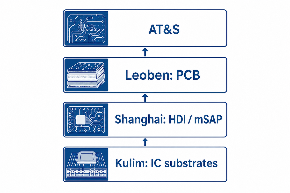
AT&S manufactures high-end printed circuit boards and IC substrates at facilities with diverse technical roles. Published location information helps buyers distinguish a PCB program from semiconductor packaging work. A useful inquiry names the construction and application first, then asks which site has the released process and production route for that work.
Established and headquarters: According to official records, the company was founded in 1987. Group headquarters are located in Leoben, Austria. Earlier dates associated with individual factories refer to the history of the factories. This has nothing to do with the inception of AT&S.
Enterprise, products and applications: AT&S is an international manufacturing group; its Leoben site lists multilayers, HDI boards and embedded power solutions. Shanghai indicates HDI and mSAP PCB production. Kulim’s high-end IC-substrate work is a separate product category. It shouldn’t be used to populate a bare-PCB capability table. Published applications vary by site and include industrial, automotive, communications and computing applications.
Technical and quality fields: No single public group specification was established for maximum layers, approved laminates, minimum trace/space, mechanical drilling, laser vias or finishes. Embedded technology and high-frequency capability aren’t surface finishes. Obtain the plant’s material and finish selections, along with its current certificates, inspection plan and qualification evidence.
Buying advantage and caveat: The company’s site-by-site descriptions support a technical routing discussion. It’s important to treat proposed PCB construction and IC-substrate claims as separate discussions, even though both may include fine features. Purchasing teams should focus on the offered process, factory and acceptance criteria and shouldn’t borrow a higher number from another division.
Official website: https://ats.net/
Mixing PCB and substrate specifications may approve a construction that the proposed line hasn’t released. Changing the process late may require new artwork or qualification, so product routing should be settled before scheduling assembly.
4. Zhen Ding Technology
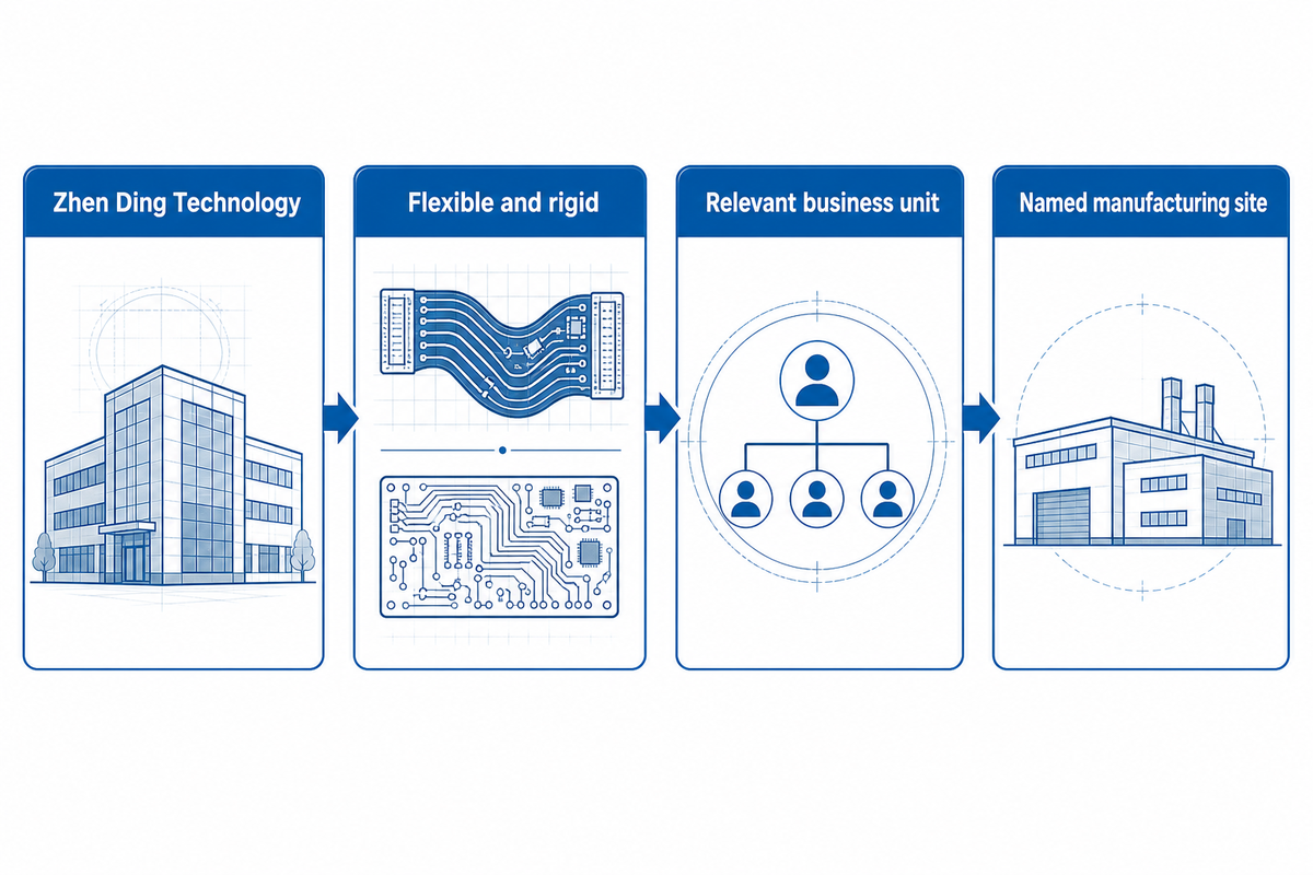
Zhen Ding Technology offers a range of interconnect solutions comprising flexible circuits, HDI, substrate-like PCBs, and rigid boards. Buyers with needs spanning multiple board families will likely find Zhen Ding Technology an attractive option. The first call should be placed to the relevant business unit and the manufacturing park, since a group product list won’t target a specific order.
Established and location: The company profile indicates 2006 as the year the company was founded. The sources checked haven’t established the current group headquarters address. Fuyong, Shenzhen, as a manufacturing location, can’t automatically be the headquarters.
Enterprise and products: Zhen Ding describes design-in, research, manufacturing and sales services. The company’s range of products includes FPC, SLP, HDI and rigid PCBs, IC substrates, rigid-flex and modules. Since the company’s products address various interconnect needs, the purchasing brief should segregate a flexible cable-like circuit from a rigid multilayer board or a packaging substrate.
Specifications, applications and quality: At the group level, material grades, layer ceilings, trace/space minima, drill sizes, finishes, and test coverage weren’t verified as one common specification. Neither a product image nor factory announcement provides an application qualification. Please request the selected manufacturing site’s approved material list, quality system, and inspection criteria.
Buying advantage and caveat: Multiple related product families can be discussed within the group. This can help in routing a complex program, but the buyer still has to have the specific construction approved. A technology roadmap, planned expansion, or new manufacturing park doesn’t demonstrate available capacity for the requested timeline.
Official website: https://www.zdtco.com/
An inquiry sent to the wrong product group might result in an incomplete response. Please name the board family and required production site to avoid material or test requirements being discovered only after the commercial approval.
5. Unimicron
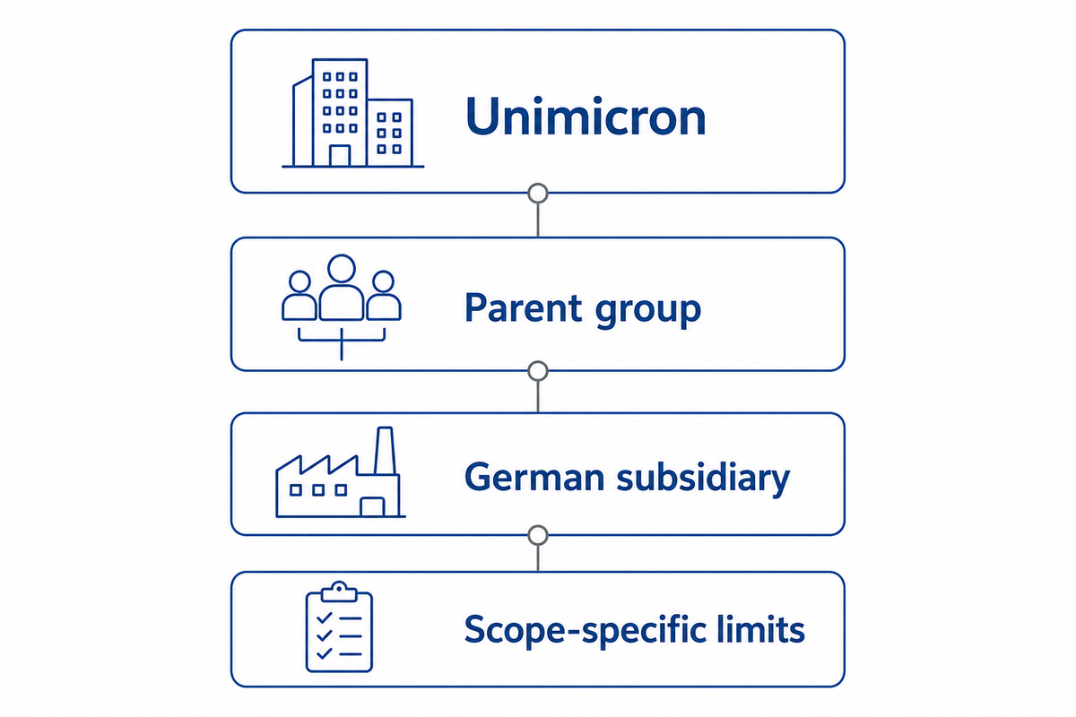
In the company information provided through the Taiwan Stock Exchange, we’ve identified Unimicron as a PCB and IC-substrate manufacturing group. Their German subsidiary provides a PCB service offering. Consider regional and corporate scopes of the offerings as the German operation’s layer count is meant for that scope, but it isn’t the confirmed limit for the group as a whole.
Founded and Headquarters: No confirmed founding year or current parent headquarters address was available on the primary pages reviewed for this report. Listing date for an exchange doesn’t mean a founding date. Unimicron Germany identifies Geldern, Germany; however, this isn’t the location of the parent in Taiwan.
Enterprise, Products and Applications: The exchange-hosted profile describes PCB and substrate manufacturing with sites in Taiwan and China. The subsidiary in Germany describes double-sided and multilayer boards, HDI and semiflex, and has applications in the automotive, renewable energy and industrial sectors.
Technical Scope and Quality: Unimicron Germany publishes multilayer production to 24 layers. The sources assessed didn’t define a group-wide standard of trace/space, mechanical-drill, laser-via, laminate or surface finish. The quality system should be assessed for the actual factory and order for each subsidiary, rather than assuming a group-wide quality transfer.
Buying Advantage and Caveat: Regional sourcing can create supply-chain efficiencies. For a proposed 24-layer inquiry to Germany, determine if the complete stack-up, finish and test are contained within the scope of the individual Germany operation’s quoted process. The purchase order should define the manufacturing origin and assign responsibility for any transfer to another group or partner site.
Official website: https://www.unimicron.com/
There can be a lot of confusion between the German subsidiary and Taiwan parent that may result in unfulfilled requirements for manufacturing. This should be avoided by including the manufacturing site, supplying entity and approved construction in the quotation.
6. Compeq
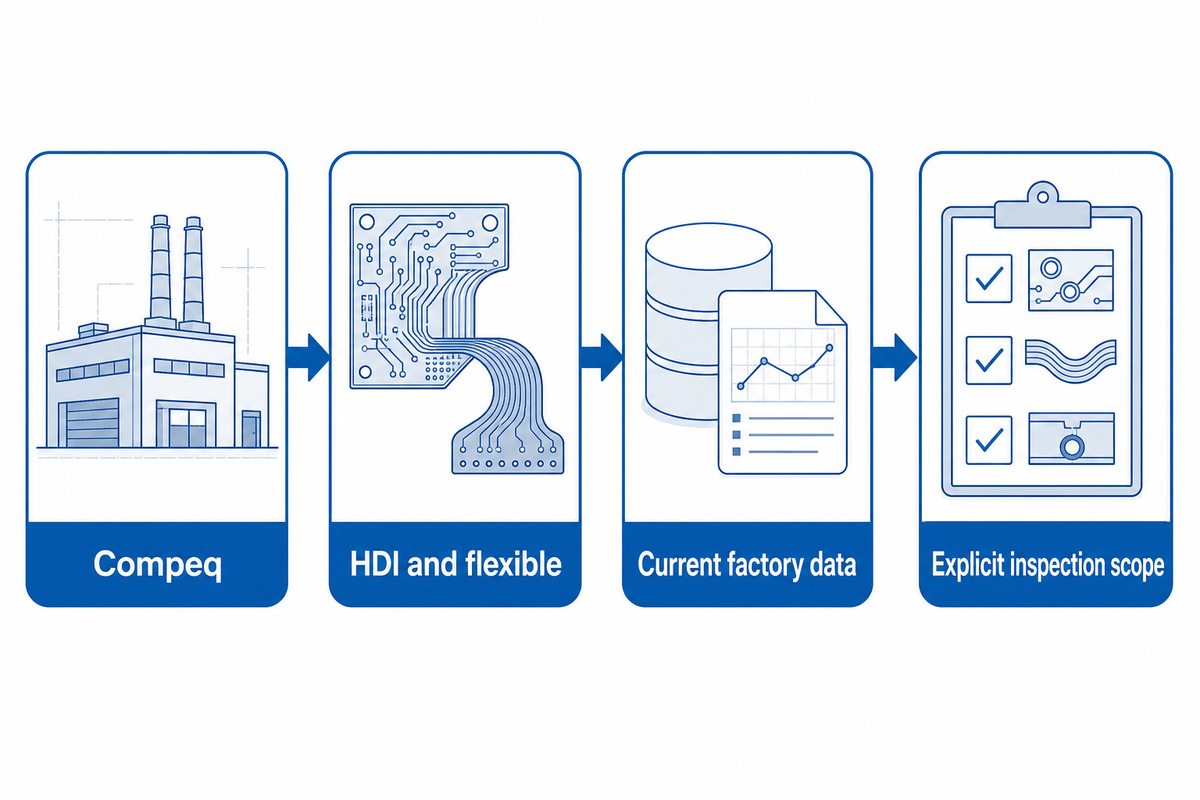
Compeq is a multilayer builder in Taiwan, focusing on HDI and flexible constructions. Compeq should be on the buyer’s radar when engaged in a conversation pertaining to a defined electronics production program. For a quote to be valid, factory data should be current, as historical reports outline product families and don’t set the limitations of factory for today.
Established and headquarters: Compeq states that it was founded in August 1973 in Luzhu, Taoyuan, Taiwan. Corporate reporting identifies the Luzhu plant as headquarters and describes additional manufacturing or service locations.
Enterprise, products and markets: General multilayer boards, HDI, high-layer-count boards, FPC, and rigid-flex, with SMT services available for customer requirements, are listed in published corporate materials. Applications described in the reporting include computers, communications, and networking as well as consumer electronics. Historical descriptions provide insight into the type of the business, but don’t indicate present allocations of different products to each plant.
Specifications and inspection: A current universal maximum layer count, material menu, minimum trace/space, mechanical-drill or laser-via size and surface-finish list haven’t been established. Request the capability sheet from the offered site and its quality-system scope. Bare-board electrical testing, microsection requirements and any assembly inspection should be explicitly stated.
Buying advantage and caveat: The published mix gives a purchasing team several interconnect families to consider. Older corporate product lists shouldn’t be considered released manufacturing specifications. Confirm the proposed construction and revision with engineering before procuring price comparisons when another supplier is offering different materials or via structures.
Official website: https://www.compeq.com.tw/
Outdated product descriptions can hide a mismatch with the process offered today. Requesting a current capability statement tied to the drawing revision is the minimum needed to approve the release of a new production design.
7. Tripod Technology
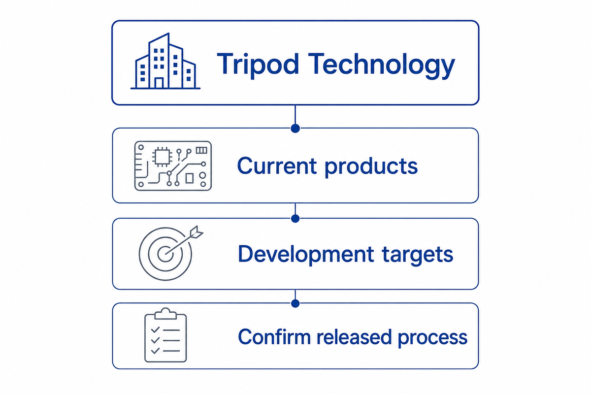
Tripod Technology markets double-sided and multilayer PCBs as its principal products. Its disclosures address research and the development of processes and technology. In this context, potential customers should distinguish the two categories. Current products may be the subject of sourcing discussions, while development targets need to be confirmed before they can be specified as requirements for a production purchase order.
Established and headquarters: Tripod dates its establishment to 1991. Its corporate reporting identifies the headquarters in the Pingzhen District, Taoyuan, Taiwan, and describes its operations in Taiwan and mainland China.
Enterprise and products: The company is a PCB manufacturer serving domestic and overseas customers. Its development discussion includes dense interconnect, high-speed and thermal applications. These plans shouldn’t be converted into an unconditional list of released production capabilities or qualified end markets.
Technical and quality fields: The research material distinguishes planned 12/16-layer HDI constructions and fine-line development from the current core product description. A 30/30 μm development reference doesn’t prove an available production process. Current laminate grades, finishes, mechanical-drill and laser-via minima, inspection methods and certificate scope need a factory-specific response.
Buying advantage and caveat: Distinguishing between products currently available and development work aids in answering technical questions. Will the requested feature be normally built, recently made available for building, still under qualification, or still in research? For fine-line work, request the approved construction and acceptance plan as an orderable specification rather than citing a roadmap number.
Official website: https://www.tripod-tech.com/
The risk is confusing a development result with repeatable production. If the proposed feature is still under qualification, procurement needs that limitation in the offer rather than learning about a delayed release after the build has been scheduled.
8. Meiko Electronics
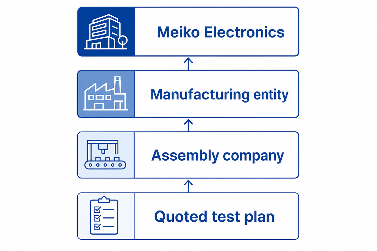
Meiko Electronics manufactures PCBs and conducts other electronics businesses through different group companies. Its published product portfolio includes both simpler through-hole boards and more complex HDI, flex, thermal, and embedded constructions. The buyer’s task is to identify the manufacturing entity for the board and the separate scope of any requested mounting or assembly work.
Established and headquarters: Meiko gives November 25, 1975, as its establishment date. The headquarters are located in Ayase, Kanagawa, Japan. The profile of the corporation highlights PCB manufacturing entities in Japan, China, and Vietnam and distinguishes these entities from sales and assembly companies.
Enterprise, products and applications: Company products include double-sided and multilayer through-hole PCBs, HDI, flexible and flex-rigid boards, high current and heat dissipation boards, and embedded device PCBs. Stencils and PCB testers appear in the company’s product list; manufacturing test equipment doesn’t describe the inspection plan that comes with the customer’s boards.
Specifications and Quality: no common group-wide limit was established for layers, trace/space, mechanical drilling, laser vias, materials or finishes. The kinds of applications and the level of certification depend on the company and the construction selected. Request from the factory that proposes the contract, the relevant quality documents and the actual tests included in the offer.
Buying Advantage and Caveat: within the group, fabrication of PCBs along with some downstream electronics services can be negotiated. Confirm where each service is performed and which organization manages the non-conformance process. A heat-dissipation product label must have a known material and a defined stack-up to be compared with another supplier’s thermal board.
Official website: https://www.meiko-elec.com/english/
Fabrication and assembly at different entities can create an inspection handoff gap. Define who reviews the bare boards, who investigates defects and which organization authorizes material or process changes.
9. Kinwong
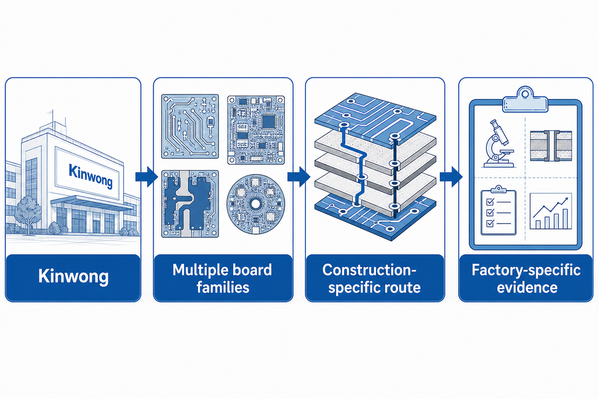
Kinwong has several standard and specialized PCB families that are produced in multiple locations. Their offerings include flexible, metal-base, HDI and RF constructions and therefore require construction-specific routing. Clients should check which factory will handle the quoted combination of materials and processes before considering the broad corporate portfolio as evidence of a single manufacturing capability.
Established and location: Kinwong was established in 1993. English language profiles confirm the PCB manufacturing plants located in Shenzhen, Longchuan, Jishui and Zhuhai. The current corporate head office wasn’t identified from the English profiles. Factory locations shouldn’t be substituted for the corporate head office.
The company manufactures conventional, flexible, metal-base, rigid-flex, HDI, high-layer-count, RF, copper-inlay and SLP PCBs, as well as engineering related services. Published client segments include Automotive, Telecommunication, smart terminals, industrial and medical electronics, consumer products, computers and power supplies.
No single maximum layer count or one trace/space, mechanical-drill and laser-via limit is stated for all those PCBs. The selected site’s documentation must be referenced to determine material grades, surface finishes, certificates and inspections. A medical market label alone doesn’t establish a specific medical quality-system qualification.
Buying advantage and caveat: A potential advantage for buyers is that they can investigate several board technologies through one group. It’s important to separate thermal metal-base or copper-inlay requirements from fine-line HDI assumptions. Reasonable quotes state the laminate, copper construction, tolerances and test plan together instead of combining unrelated minima from different PCB families.
Official website: https://www.kinwong.com/
Substituting materials may introduce impedance or assembly process incompatibility even though board dimensions are nominal. Require engineering approval of alternatives prior to acceptance of an unspecified equivalent laminate.
10. Shennan Circuits
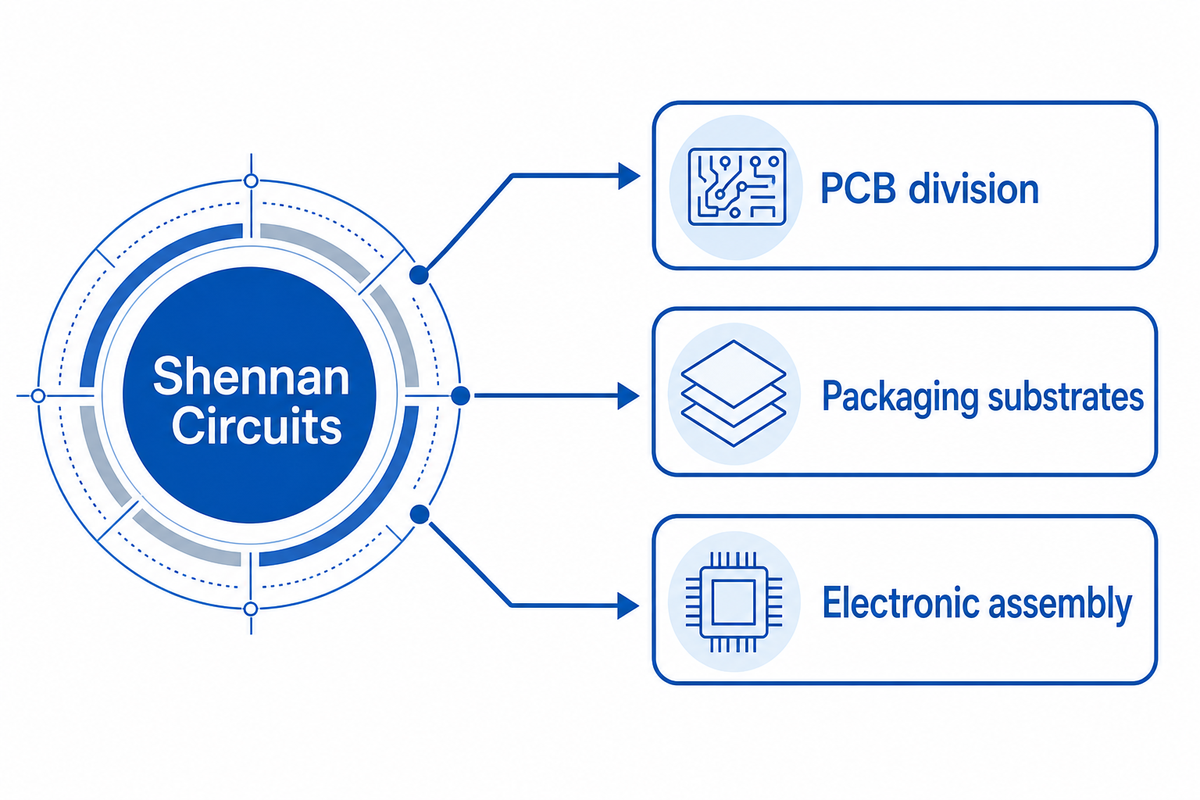
The combination of Shennan Circuits’ PCB business, packaging substrates, and electronic assembly forms several entry points for a technical inquiry, but product categories should be kept separate when qualifying. A bare board buyer must obtain construction and factory details pertaining to the PCB division before making substrate or assembly claims when comparing suppliers.
Established and Headquarters: Shennan mentions that it was founded in 1984 and is headquartered in Shenzhen, China. The introduction of Shennan indicates that there are manufacturing facilities in Shenzhen, Wuxi and Nantong. The other overseas subsidiaries and research centers serve different functions than the factories.
Enterprise, products and applications: The group mentions that PCBs are its core business, but packaging substrates and electronic assembly are included. Their introduction mentions relationships with communications and medical equipment customers. These relationships describe the business, but they don’t confirm that every construction or facility has a particular application certification.
Specifications and Quality: One common layer ceiling, laminate list, trace/space minimum, mechanical-drill size, laser-via size and surface-finish menu weren’t established from the corporate overview. The buyer must contact the quoted business unit for these. A quality-system link is an invitation to review the certificate, including the certified site and validity period.
Buying advantage and caveat: Specifications for PCB, substrate, and assembly can be discussed with the relevant businesses. For each deliverable required, obtain an explicit quote. The feature size of an IC-substrate doesn’t necessarily mean that the same size is also available for a large, bare PCB of different materials and layer construction.
Official website: https://www.scc.com.cn/
When requirements are too general, PCB specifications can become part of the discussion regarding substrates and assembly. Avoid the mismatch in the requested scope by listing bare-board acceptance criteria and the supply of components and packaging before the first comparison of quotes is made.
11. WUS Printed Circuit, Taiwan
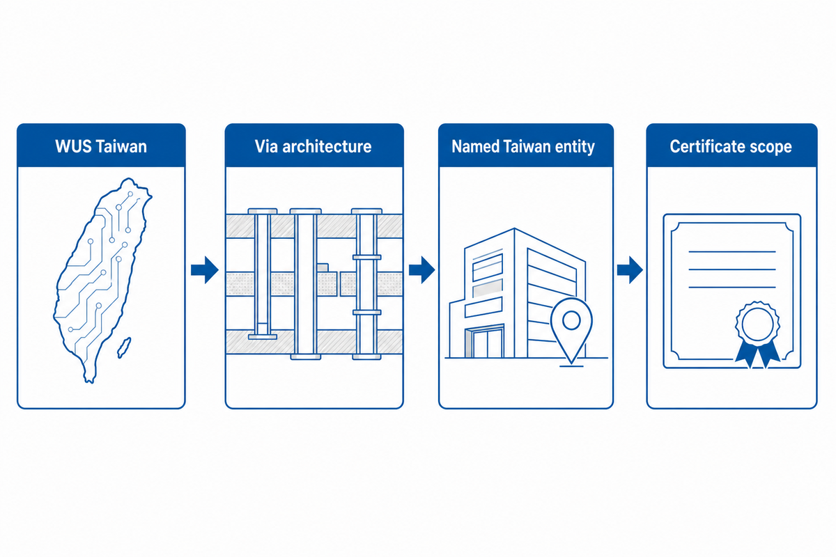
WUS Taiwan publishes HDI and high-speed PCBs, along with specific via-architecture options. Compared to layer count, these provide a better starting point for engineers. The Taiwan company and the proposed manufacturing site must be specified by buyers, as similarly named operations and certificates from other regions must not be treated as substitutable.
Established and location: The official history dates WUS Taiwan to 1972. The street address of the headquarters in the primary source checked was not confirmed. This profile concerns the business at wus.com.tw, not a different company inferred from the WUS name.
Enterprise, products and applications: WUS describes PCB manufacture for demanding electronic applications, including industrial and medical requirements. WUS technology information lists HDI build-ups from +1 to +8, and 4–18-layer any-layer HDI. Published process options include plated-over filled vias, stacked or skip vias, back-drilling and embedded passive components.
Materials, limits and quality: The site describes high-speed, low-loss materials without providing one universal approved-grade list. Trace/space, mechanical-drill and laser-via minima and surface finishes require construction-related assurances. A certificate for a Thai manufacturing entity can’t be used to support that the Taiwan entity or every group plant has the same certified scope.
Buying advantage and caveat: The mentioned HDI structures prompt detailed questions from the designer about via position and lamination ordering. An 18-layer any-layer inquiry still needs material, copper and reliability requirements approved together. Ask which factory will do it and how the selected via interfaces will be qualified for the intended assembly profile.
Official website: https://www.wus.com.tw/
Using a certificate from the wrong entity creates a qualification gap. For stacked vias, also ask how latent interface failure is addressed; normal continuity checks don’t provide answers to all the reliability concerns.
12. Nan Ya PCB
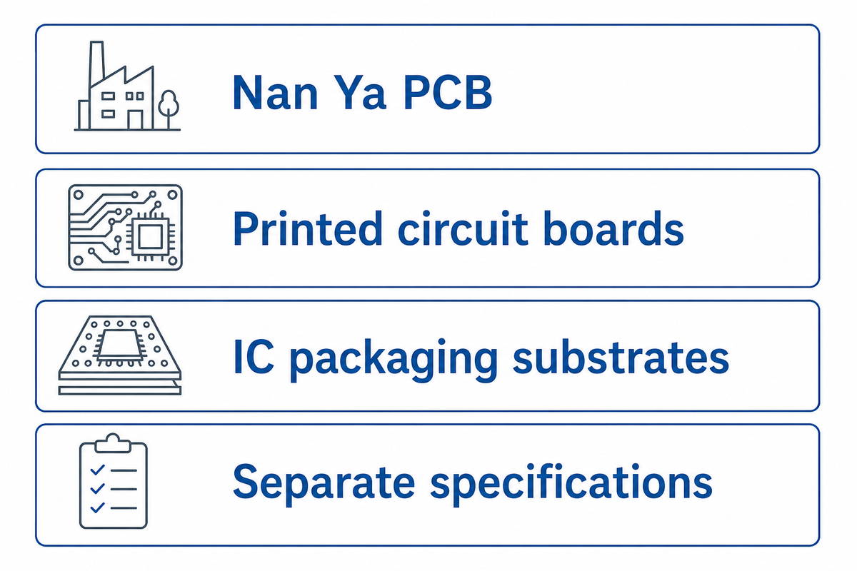
Nan Ya PCB manufactures printed circuit boards and IC packaging substrates as separate product families. Corporate information clearly distinguishes the head office from manufacturing locations. Buyers can use that distinction to draft an inquiry, and then examine the specific PCB or substrate path rather than assuming that all published technologies share the same fabrication limits.
Established and headquarters: The company gives October 1997 as its establishment date. Its head office is in Neihu District, Taipei, Taiwan. Jinshing in Taoyuan, Shulin in New Taipei and Kunshan are listed separately as manufacturing locations.
Enterprise and products: Nan Ya publishes conventional PCBs, HDI, rigid-flex, ABF substrates and PP substrates. ABF and prepreg substrate descriptions identify packaging-product categories; they don’t establish a finished bare-board material specification or a universal feature size.
Applications, specifications and quality: The corporate profile checked didn’t provide one current application-qualification list, layer ceiling, minimum trace/space, mechanical-drill or laser-via diameter, surface-finish menu or inspection plan. Those fields should be obtained from the relevant product organization. Current certificates need the actual production address and covered activity.
Buying advantage and caveat: The portfolio supports a discussion across PCB and packaging needs. For ordinary PCB procurement, keep substrate dimensions and tolerances out of the comparison unless that’s the product being purchased. A quote should identify the supplying entity, manufacturing location and approved construction before procurement evaluates price or delivery against another company.
Official website: https://www.nanyapcb.com.tw/
Substrate data placed on the bare-board drawing may create a misalignment of specifications. It’s advised to keep the two product categories distinct and ask the proposed factory to confirm any unverified construction requirement prior to commercial release.
13. Würth Elektronik Circuit Board Technology
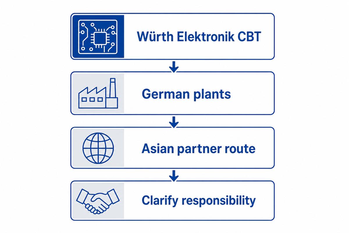
Würth Elektronik Circuit Board Technology has PCB production via German plants and qualified Asian partner routes. The structure of the business is critical when researching it; the PCB division maintains a distinct headquarters from the electronic-components division. Clients must select the sourcing route explicitly and clarify who’s responsible for engineering inspection and manufacturing quality.
Established and headquarters: The group traces electronics activities to 1971 and documents the establishment of an independent company in 1976. Niedernhall, Germany, is indicated as the headquarters of Circuit Board Technology. Waldenburg is part of the eiSos components business and shouldn’t replace the PCB business headquarters in a supplier profile.
Enterprise, products and order scope: The official company description identifies German PCB plants and qualified Asian partners. It addresses basic and advanced technologies, prototypes, medium-range and larger volumes. This is a manufacturing-and-partner model, and the route should be evident in the offer.
Note: One group-wide maximum layer count, material list, trace/space minimum, mechanical-drill or laser-via size and finish menu wasn’t established from the corporate profile. Industry suitability, certificate scope and inspection requirements need confirmation for the selected route and site.
Buying advantage and caveat: Engineering support and alternative sourcing routes can be discussed with the PCB business. A buyer requiring German manufacture should state that requirement in writing rather than relying on the headquarters address. If a later order moves to a partner facility, agree on any first-article review, material approval and test evidence before the transfer.
Official website: https://www.we-online.com/
To interpret German origin from the brand address would introduce a sourcing risk when the offer uses an Asian partner. Document the actual route and review any later factory change before relying on a repeat-order approval.
14. Eurocircuits
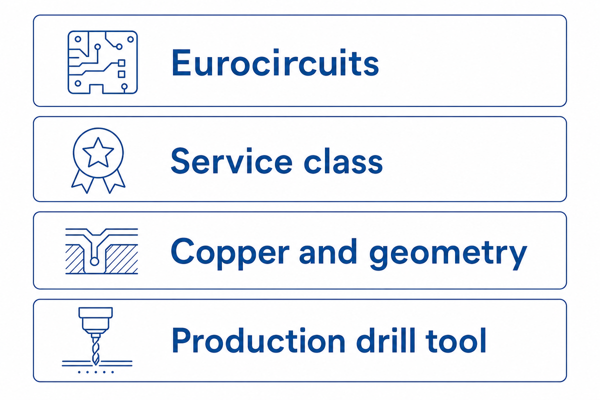
Eurocircuits specializes in the production of PCB assemblies and European PCB manufacturing for prototypes and small series. Digital tools enable customers to carry out manufacturing checks before orders are issued. As a result, service-class selection becomes a consideration when purchasing: the allowable geometry is dependent on the chosen copper and technology, rather than one minimum feature size applying to all boards.
Established and headquarters: The official anniversary account says the company was founded in May 1991, with its main office in Mechelen, Belgium. The company’s published service model describes manufacturing in Europe.
Enterprise and products: Eurocircuits manufactures PCBs and electronic assemblies, with a focus on prototype and small-batch assemblies. Visualizer tools allow customers to inspect manufacturing data and component placement, and provide a 3D view of the assembled PCB. This digital workflow can identify potential file or service class discrepancies before production, but isn’t designed to take the place of the customer’s design approval.
Technical scope and finishes: Exact layer limits, laminates, trace/space, drilling and surface finishes depend on the service class selected. The company’s classification guidance indicates that with the selection of a thicker copper, wider isolation is required. The assessment of the annular rings uses the production drill tool, not the finished hole size. Request the mechanical-drill and laser-via limits for the selected service, rather than assuming they’re available in all classes.
Quality, advantage and caveat: Visible design checks are useful for engineering teams building early-stage products. Verification of certificate scope and test records still requires order confirmation. For a board built at a service limit, confirm the manufacturing allowance prior to ordering; a drawing that fits the finished hole may still clash with the production tool and annular ring.
Official website: https://www.eurocircuits.com/
Designing directly at a service limit leaves little room for manufacturing allowances. If the production tool and finished-hole requirements conflict, resolve the discrepancy in the drawing prior to the arrival of the board to fabrication.
15. Sierra Circuits
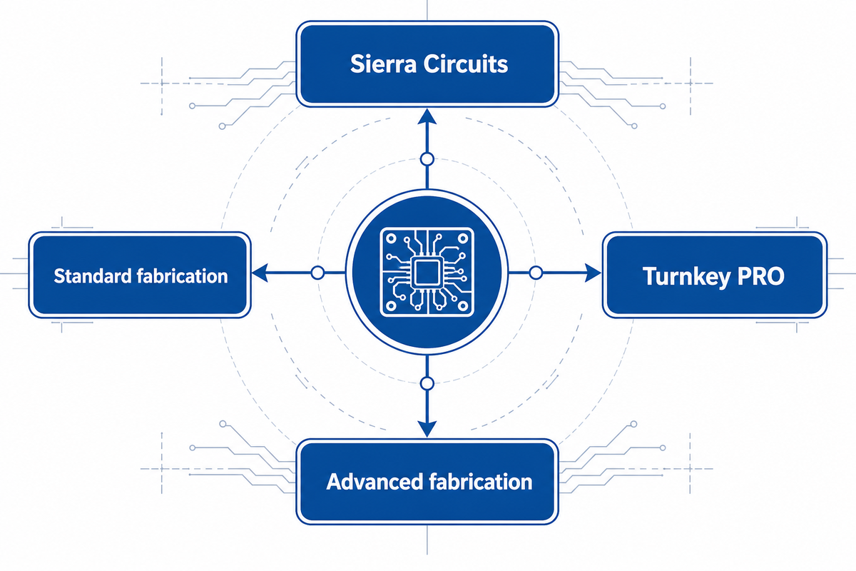
Sierra Circuits publishes US PCB fabrication and assembly services with differing capability packages. Its tables distinguish turnkey, standard, and advanced options instead of presenting one limit for every order. Buyers should select the service appropriate for the construction and check what inspection records, coupons, and certifications are included in that particular quote.
Established and headquarters: Sierra dates the start of operations to 1986 and gives Sunnyvale, California, as the location. The firm describes in-house fabrication and assembly services.
Products, materials and limits: Its published table lists 2-, 4-, 6- and 8-layer Turnkey PRO options, standard fabrication up to 12 layers and advanced fabrication up to 30 layers. Listed trace minima differ by package: 4 mil, 2 mil and 1.5 mil, respectively. A trace minimum isn’t automatically a trace-and-space guarantee.
Advanced material choices include FR-4, high-Tg, Rogers, polyimide and thermal or metal-core options. Published finishes include several gold finishes, ENIG, OSP, immersion silver and HASL. Mechanical-drill and laser-via limits should be confirmed for the selected construction. These limits shouldn’t be assumed based on a fine trace number.
Applications and quality: Product and service pages address electronics programs with different complexity and reliability needs. Test-coupon availability and documentation differ between packages. Check the relevant certificate and acceptance requirements, especially where a low-cost service doesn’t include the evidence needed by your quality team.
Buying advantage and caveat: Visible tradeoffs in package comparison should be noted. A 1.5 mil advanced trace claim can’t be carried into a standard-service quote. Compare the same layer construction and material along with the test documentation prior to assuming a lower-cost offering covers the same deliverable.
Official website: https://www.protoexpress.com/
Comparing different packages may conceal a lack of test coupons or inspection reports. This documentation gap may prevent a quality team from accepting an otherwise functional board. Thus, the price for required evidence should be negotiated with fabrication.
16. AdvancedPCB
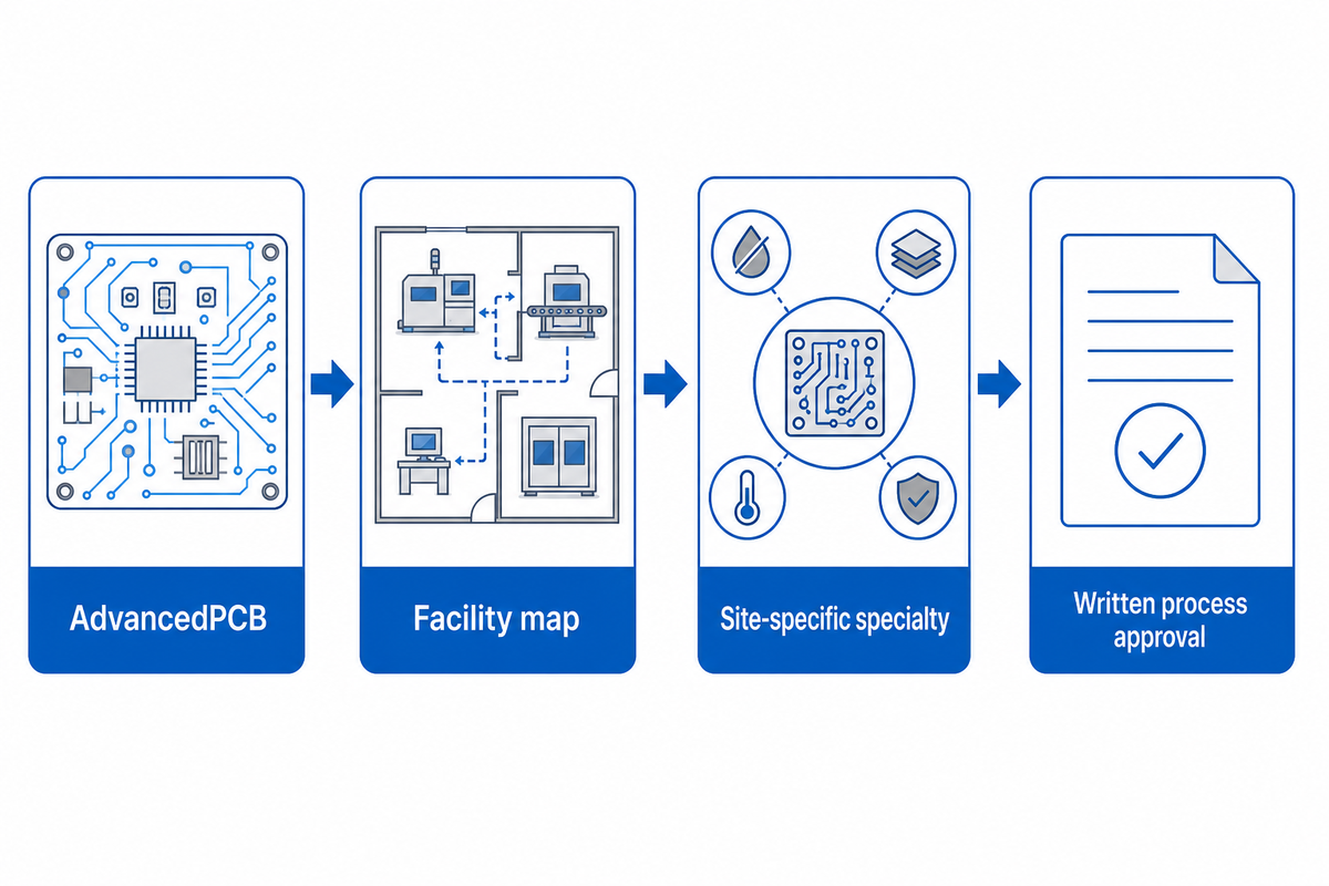
AdvancedPCB offers design and construction of PCBs along with fabrication and assembly services at several US locations. The current group comprises previous businesses. Use the facility map to route client inquiries before requesting individual capability statements for the selected locations, as the US locations have different manufacturing lines.
Established and headquarters: APCT, Advanced Circuits and San Diego PCB Design united under the AdvancedPCB name in 2024. The company’s history dates APCT to 1977. Headquarters are in Aurora, Colorado; neither date should be presented without explaining whether it refers to the current brand or its predecessor.
Enterprise, products and applications: Published facility specialties include standard fabrication and turnkey work at Aurora, HDI/UHDI at Santa Clara, flex and rigid-flex at Orange, and RF, microwave and oversized boards at Maple Grove. Such distinctions help route electronics, aerospace and other demanding programs to a relevant discussion.
Specifications and quality: Maximum layers, laminate grades, minimum trace/space, mechanical and laser drilling, finishes and testing should come from the proposed facility. Check ISO or AS9100 documents for site and activity coverage. Where applicable, ITAR status should be described as registration, not a product-quality certification.
Buying advantage and caveat: The facility map shows technical specialization. Equipment announcements also need that delineation: a 2026 vacuum via-filling installation at Santa Clara is an example of that investment, not a network-wide yield guarantee. For the actual board, require a released production process and agreed test package.
Official website: https://www.advancedpcb.com/
Capability at one facility doesn’t remove a qualification gap at another. Unapproved routing changes can delay acceptance; ask the supplier to identify the plant and flag any proposed transfer before production.
17. Summit Interconnect
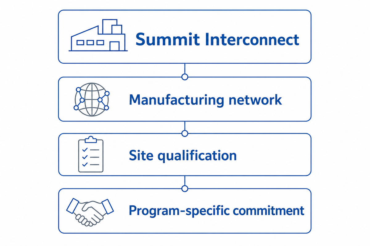
Summit Interconnect operates a North American advanced PCB manufacturing network. Group history and facility information are helpful in finding a potential production route, but procurement still needs a site-level capability statement. Buyers should identify the proposed plant and program requirements before interpreting the corporate portfolio as proof of qualification for a specific build.
Established and headquarters: Summit says it was formed in 2016 through acquisitions. The current company description identifies Irvine, California, as headquarters. An acquired factory in Anaheim is a manufacturing location, not sufficient evidence that the group headquarters are there.
Enterprise, products and applications: Summit describes advanced PCB manufacturing for programs that require demanding constructions and reliability controls. Its network should be evaluated through the relevant site’s published technologies and program experience. A corporate claim about advanced electronics doesn’t specify the material, via architecture or acceptance tests for an individual order.
Technical and quality fields: One maximum layer count, trace/space minimum, mechanical-drill size, laser-via size, laminate menu and finish list wasn’t confirmed as a universal group specification. The current quality-system certificates and inspection requirements for the manufacturing site mentioned in the offer should be obtained.
Buying advantage and caveat: There are a number of specialist operations where buyers can discuss multiple options under one roof. That advantage relies on clear ownership when work is transferred between sites. Before releasing a repeat order to another site, verify the stack up, material approvals, process changes and qualification evidence rather than assuming the same corporate name means the same construction.
Official website: https://summitinterconnect.com/
Repeat orders can introduce process differences after transfer to a factory. The risk is assuming that corporate continuity means manufacturing equivalence; the agreed materials, tests and change approval must remain visible in the order.
18. JLCPCB
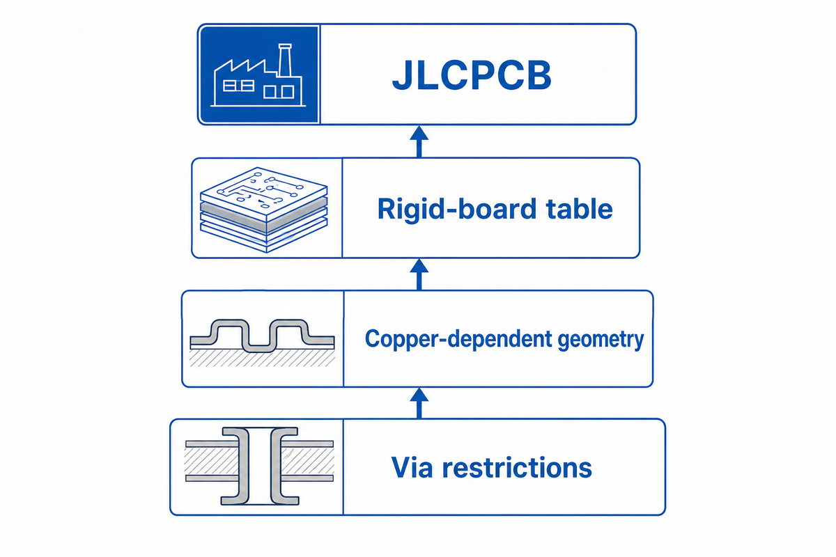
JLCPCB combines online PCB ordering with component sourcing and assembly services. The rigid-board capability table gives valuable construction-specific limits, including copper-dependent geometry and finish restrictions. Buyers should refer to the selected board family and current configurator: the maximum number of rigid layers doesn’t establish that all via configurations are supported by that service.
Established and location: JLCPCB mentions that it was founded in 2006. There’s a supplier-hosted certificate that references a Shenzhen legal entity, but a certificate address wasn’t treated as independent confirmation of the entire group’s current headquarters.
Products and specifications: The rigid table lists 1–32 layers, mainly FR-4, with separate single-layer aluminum and copper-core options and two-layer Rogers/PTFE RF constructions. For 1 oz copper, it lists 4/4 mil trace/space on one- and two-layer boards and 3.5/3.5 mil on multilayers. Two-ounce copper requires wider geometry. A 0.15 mm drill option applies to two or more layers, with its own pricing and construction conditions.
Finishes, inspection and applications: HASL, ENIG and OSP appear with exclusions by material, thickness and layer count. The rigid table explicitly excludes blind/buried vias in the scope of the service. Check the test package and current certificate for the chosen product; an online ordering option isn’t an application qualification.
Buying advantage and caveat: Published tables and digital ordering make standard prototype PCB specifications more accessible. A 32-layer offering alone isn’t proof of any-layer HDI. Keep component sourcing and assembly requirements separate from the bare-board specification, especially when BOM and component availability drive delivery.
Official website: https://jlcpcb.com/
Configurator mismatch can invalidate a quoted price before engineering release. Check the selected copper and via options together, particularly when a design changes from 1 oz to 2 oz copper or uses 0.15 mm holes.
19. PCBWay
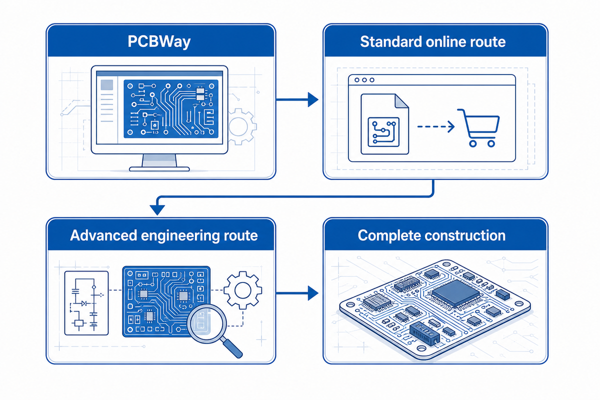
PCBWay’s website provides an online service for fabrication as well as the more complex engineering and PCB assembly routing. PCBWay’s capabilities page distinguishes simple order processes from more complex constructions. This can be used to evaluate incoming requests for both prototyping and production, so long as the customer provides the complete combination of the material, geometry and the required inspection, instead of choosing isolated maximums from different tables.
Established and location: An exact founding year wasn’t confirmed from the official pages checked. The OEM information identifies a Hangzhou head office, while capability information describes Shenzhen production. Be sure to confirm the contracting entity and manufacturing address rather than assuming that an office or payment entity identifies the factory.
Products, materials and limits: The standard table lists 1–14 layers, FR-4, aluminum and copper-base options, 4 mil minimum trace and spacing, and CNC drilling from 0.15 mm. HDI, flex, rigid-flex and specialist materials follow the advanced route. Material availability and process difficulty can change the offer.
Finishes and quality: Published options include leaded and lead-free HASL, immersion gold, OSP, hard gold, immersion silver, immersion tin and ENEPIG, subject to construction review. PCBWay describes AOI and electrical testing, with flying-probe and fixture approaches for different volumes. An obsolete ISO 9001:2008 reference still present on a capability page should not be used as current certificate evidence.
Buying advantage and caveat: The division of standard and advanced offerings helps buyers identify when an online configuration requires engineering review. A 0.15 mm drill minimum doesn’t establish an acceptable aspect ratio at every board thickness. Request the latest quality documents and a drilling/stack-up approval for the quoted route.
Official website: https://www.pcbway.com/
An old certificate reference creates a verification gap, while a small drill can create a separate construction risk. Consider both current quality documents and the approved thickness/drill combination as separate items to close.
20. QueenEMS
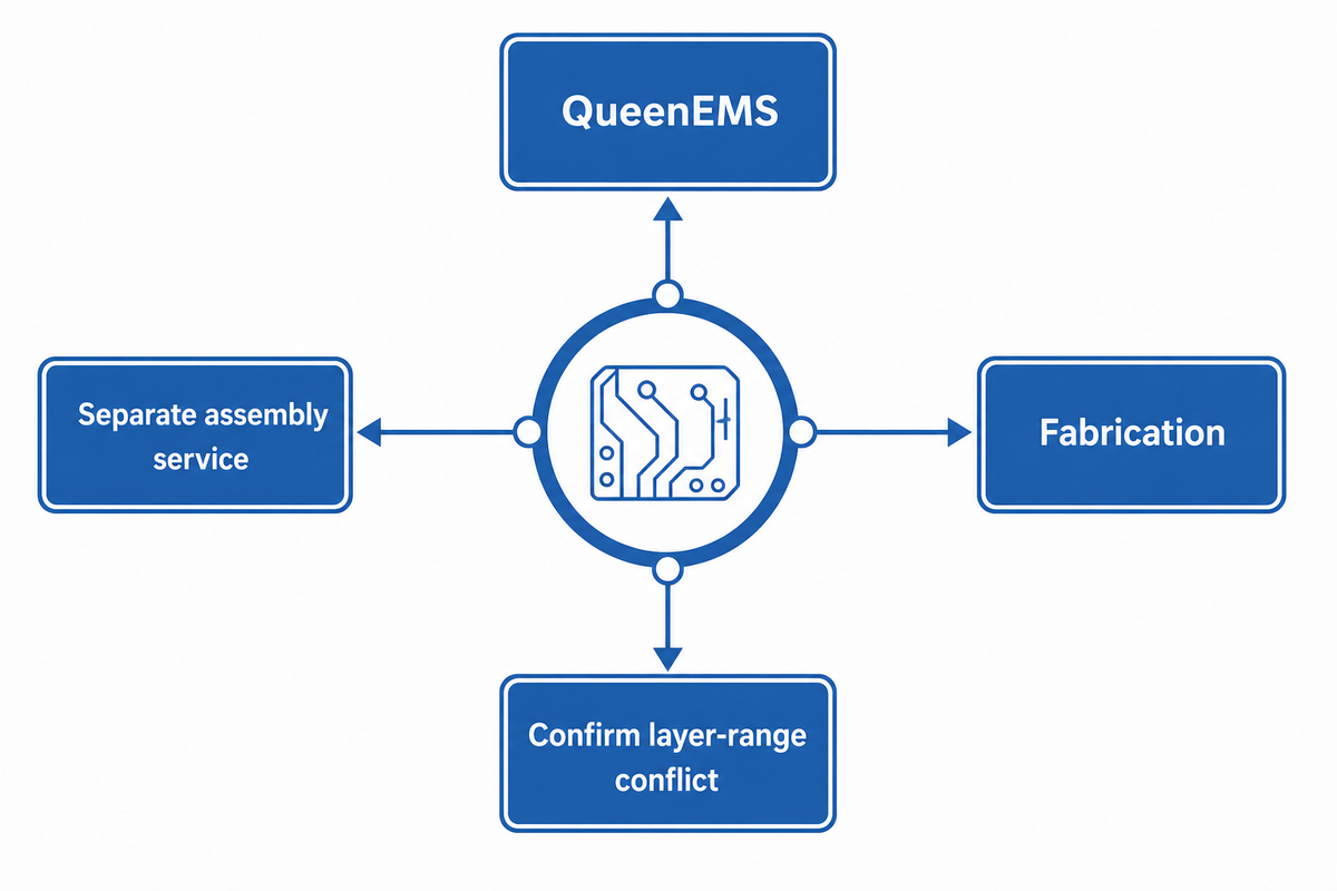
QueenEMS indicates that custom bare board fabrication is a core service, with assembly available as a separate service. Public pages present several ranges of product-specific capability, but the figures for layer don’t agree all the time. Therefore, the best way to contact the company is to ask for a construction-specific response (defining the entire stack-up), identifying the responsible party for manufacturing.
Established and location: The company claims more than ten years of experience, but doesn’t provide an actual founding year. The site lists a Shenzhen factory and a Bangkok “Head Office.” Confirm which entity accepts the order and where fabrication and assembly will occur.
Enterprise, products and specifications: QueenEMS indicates that it provides imaging, lamination, CNC drilling, plating/etching and electrical testing in-house. The homepage mentions standard capability up to 24 layers and advanced capability up to 60, while another table provides 1–40 layers. Different ranges specify 1–6 layer flex and 4–22 layer rigid-flex. These can’t be merged into one guaranteed capability.
Materials, finishes and testing: RF and other constructions require an approved laminate. Published drilling data distinguish 0.15 mm mechanical holes from 0.075 mm laser vias; a minimum trace/space wasn’t verified. ENIG, ENEPIG and hard-gold are listed. A sample quality report indicates a format for a lot rather than a company-wide yield or a factory audit.
Buying advantage and caveat: Buyers can discuss bare boards and assembly as a group. Resolve the layer-range conflict and obtain current, site-specific quality documents to qualify. The QueenEMS custom PCB fabrication and assembly website is provided here through a reciprocal link exchange with PCBark. No reciprocal placement has been verified in this article.
Ambiguous layer ranges can lead to a scope mismatch between an inquiry and a quotation. Require one construction, its material, via geometry and testing; the exchange relationship doesn’t remove that technical qualification step.
How to compare PCB manufacturers without combining incompatible specifications
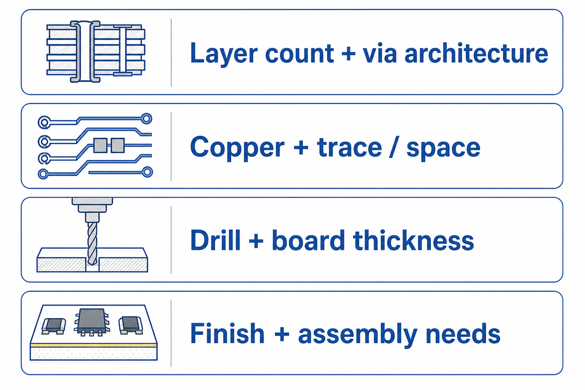
Analyze a complete PCB construction rather than isolated manufacturing limits. Different variables including layer count, copper, laminate, drill geometry and finish mean that the most impressive number on each supplier’s webpage could describe a completely different process. Request engineering to sign off on the combination and request quality to define the evidence that will be included with the complete boards.
The Specification Combination Check below has converted some marketing fields into engineering specification questions. For HDI-only sourcing, the separate HDI supplier comparison provides a more focused route. This general list doesn’t replace that technical selection exercise.
| Field | Read it together with | Evidence to request |
|---|---|---|
| Layer count | Via architecture and lamination sequence | Approved stack-up, including blind, buried or through vias |
| Minimum trace/space | Starting and finished copper, inner versus outer layers | Geometry approval for the selected copper construction |
| Mechanical holes | Board thickness, finished-hole tolerance and plating | Drill table and accepted manufacturing allowances |
| Laser microvias | Dielectric thickness, via interfaces and assembly exposure | Construction-specific qualification and test plan |
| Laminate | Electrical, thermal and assembly requirements | Manufacturer, grade and permitted substitutions |
| Heavy copper | Etching geometry, clearances and thermal design | Combined copper/spacing capability confirmation |
| Controlled impedance | Stack-up, finished copper and material data | Approved geometry and agreed coupon/report requirements |
| Surface finish | Assembly process, contacts and shelf-life needs | Finish specification, thickness and applicable acceptance |
| Quality system | Legal entity, factory address and covered activities | Current certificate and scope, checked at the source |
| Electrical testing | Netlist, quantity and defect mechanism | Agreed test coverage, method and lot records |
| Lead time | Material availability and engineering release | Start condition, production commitment and shipping scope |
| Assembly | BOM, component placement and functional requirements | Separate PCBA scope and inspection/test instructions |
NIST defines process capability in terms of stable production and specification limits, not a successful sample on its own. Its statistical guidance provides a useful distinction between making a feature once and demonstrating a controlled process:
“A process capability index uses both the process variability and the process specifications to determine whether the process is ‘capable’”
There are limits to PCB inspection. In its 2019 microvia reliability warning, IPC documented failures that occurred after the traditional production-lot acceptance. This historical evidence doesn’t implicate any of the companies in this list in producing defective work. It shows why a continuity pass or microsection, among other things, may not fully answer all the reliability concerns for a demanding via construction.
Illustrative copper example: An engineer has a 4-layer FR-4 design using 1 oz copper and 4/4 mil routing, then changes the request to 2 oz copper for a power revision. Procurement sends the original drawing to three vendors to check for pricing and compares the proposals received. The copper change can alter the allowed geometry; the old drawing is no longer an adequate common basis. JLCPCB’s published table, for example, lists wider spacing for 2 oz than for 1 oz. It is best to get the engineering team to approve the copper and the geometry together before sending in a request for new quotes. That prevents an apparently cheaper supplier from silently quoting a different manufacturable interpretation.
Illustrative drilling example: A buyer specifies a 0.20 mm finished hole in a 1.6 mm board but leaves plating, tolerance and pad geometry unresolved. Another quote uses a different production tool size and allowance. Dividing 1.6 mm by 0.20 mm gives a geometric ratio of 8:1, but this simple calculation isn’t a supplier’s approved drilling or plating capability. The relevant manufacturing definition and limits still need to be agreed on. Eurocircuits differentiates tool size from finished hole size when considering annular rings. Send the finished-hole requirement and let the fabricator return the approved production interpretation; don’t substitute a calculator result for engineering acceptance.
For a complete account of the fabrication stages, please refer to the bare-board manufacturing process guide. Keep this supplier comparison focused on the construction, factory, and evidence required for making a purchase decision.
Send one build package before comparing PCB quotes
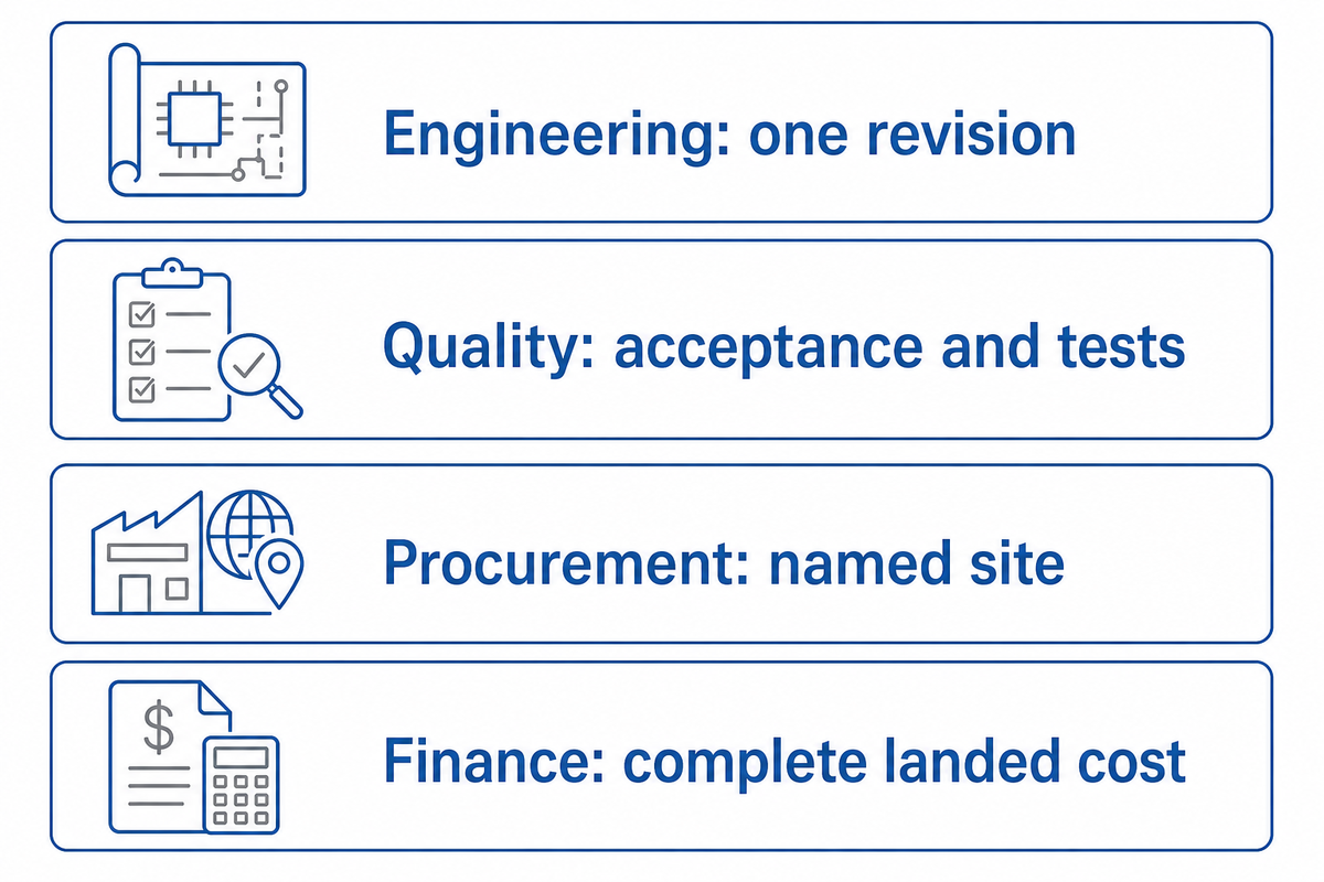
A reasonable PCB quote comparison treats all suppliers the same by providing the same released files, construction and acceptance criteria. Separate bare-board fabrication from assembly, and list all unresolved issues. Then, purchasing can compare the cost and lead time for the same delivery, instead of evaluating competing offers that tacitly imply different materials, tests or manufacturing locations.
The One-Build RFQ Comparison Sheet is a helpful template for engineering, quality and purchasing to pass on one narrative with one revision of the drawing and one answer log for the complete shortlist. If a supplier proposes a change, note it as an exception rather than revising only that supplier’s document.
The best PCB manufacturers for a certain project are the ones that are able to meet all of its requirements. Treat a search for the best PCB fabrication service as a starting point, then assess the accepted construction and evidence. A printed circuit board assembly service also requires components and placement information; printed circuit board assembly services are unable to give an accurate price for this service based on just bare-board drawings.
| Owner | Send or confirm | Compare in the replies |
|---|---|---|
| Engineering | Gerber file set or agreed data format, outline and revision | Exact revision accepted, open engineering questions |
| Engineering | Layer stack-up, laminate grade, finished thickness | Accepted construction and every proposed substitution |
| Engineering | Copper, trace/space, mechanical drills and microvias | Combined manufacturability, tolerances and exceptions |
| Engineering | Impedance, solder mask, silkscreen and finish | Agreed values, measurement and inspection methods |
| Quality | Acceptance standard, revision, class and applicable addenda | Offered compliance and documented exceptions |
| Quality | Electrical and application-specific reliability tests | Included tests, coupons, reports and sample requirements |
| Quality | Traceability and change-approval requirements | Lot records, material identity and approval process |
| Procurement | Quantity, delivery destination and required date | Production start condition, shipment and commercial scope |
| Procurement | Named manufacturing site and subcontracting disclosure | Origin, responsibility and any transfer conditions |
| Assembly engineering | BOM, component placement, stencil and test instructions | Component substitutions, assembly scope and test coverage |
| Finance | Common currency and complete landed-cost assumptions | Tooling, test fixtures, freight and other separately charged items |
Incomplete purchasing specifications could include fast PCB manufacturing or low-cost PCB prototyping and manufacturing. Define when the clock starts: is it when a file is uploaded, when a payment is made, when the materials are available, or when engineering is released? The quotation needs to define the time required for the production and the time required for transport, and neither should be implied from a homepage promotion.
Illustrative production-transfer example: A team orders 20 prototype boards to verify connectors and firmware, then prepares a 2,000-board production batch. The prototype powers up, but the larger order introduces a different factory and a substitute laminate. This is a new qualification challenge, even if the circuit and supplier brand remain the same. Engineering should review the stack-up and assembly exposure; quality should agree on traceability, coupons and any reliability work required by the application. Procurement can then compare the cost of keeping the approved route with qualifying the alternative. The first 20 working boards establish limited functional evidence, not automatic approval of the new production process.
Use the acceptance-class comparison to prepare for the quality discussion. Name the agreed standard and revision in the drawing. An ISO certificate pertains to the management-system scope. An IPC class pertains to the specified product acceptance. Neither can replace the other.
Industry outlook: qualify the available process, not the announcement
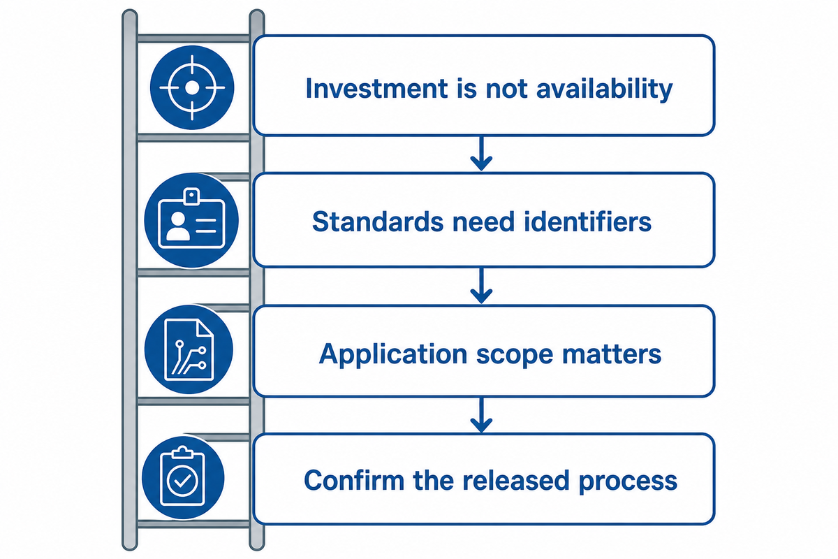
PCB sourcing in 2026 includes factory investment and updated technical requirements, but an announcement doesn’t establish a buyer’s available production route. Treat new equipment, capacity and standards as reasons to ask better questions. Verify that the offered site has released the required process and provides the agreed materials and acceptance evidence.
For 2026, AdvancedPCB announced equipment to fill vias with vacuum in Santa Clara, and announced drilling equipment at other named facilities. These announcements pertain to the individual plants and don’t provide comparable statistics for this shortlist. The primary concern is whether the equipment supports the quoted construction and whether the equipment qualification is complete.
Standards also require specific identifiers. The official IPC revision table identifies IPC-6012F, along with separate application addenda. In their public description of revision F, IPC outlines changes regarding rigid-board qualification and microvia reliability. Customers must indicate the base document and the applicable addenda over simply writing “IPC compliant.”
The NASA standard record on revision A of NASA GSFC-STD-8001 dated August 24, 2026, covers high-reliability PCBs for GSFC project mission hardware. As stated on their record, it isn’t a NASA Mandatory Standard. The Goddard standards register provides the context of this document. This is an application-specific reference and does not automatically apply to every commercial board.
No market-growth percentage or world production ranking is inferred from these developments. A manufacturer’s released process, current material availability, and a written quote are the evidence for a delivery commitment.
Frequently asked questions
What is the best PCB manufacturer?
There’s no single best PCB manufacturer for every board. Start with the required stack-up, laminate, copper thickness, minimum features, acceptance criteria and order quantity. Then compare suppliers that can confirm the complete combination at the intended factory. A prototype price or a headline process limit can’t establish repeat-production suitability. Ask engineering and quality teams to review the same fabrication package before procurement compares quotations.
Who are the top 10 PCB manufacturers in the world?
A defensible top-ten ranking needs a defined measure, reporting period and comparable company data. Revenue, bare-board sales, package-substrate sales and technical specialization can produce different lists. This article instead presents twenty suppliers for engineering comparison, with PCBark first by editorial request. Readers should shortlist companies by verified product and factory scope rather than treating presentation order as an independent market-share or quality ranking.
Who are the major PCB manufacturers in the USA?
Several companies in this comparison publish United States PCB fabrication operations, including TTM Technologies, AdvancedPCB, Summit Interconnect and Sierra Circuits, subject to verification of the specific manufacturing facility. A company’s headquarters alone doesn’t prove where a particular order will be built. Ask the supplier to name the production site, identify any subcontracted processes and provide the applicable quality-system and inspection documents for your project.
Is PCB fabrication the same as PCB assembly?
No. Fabrication produces the bare printed circuit board; assembly places and solders components onto it. A supplier may offer both, but each service needs its own scope, files and acceptance criteria. Board drawings define fabrication; component placement data guides assembly.
What should I send for a PCB quote?
Provide the Gerber file set or an agreed manufacturing data format, fabrication drawing, board dimensions, quantity, stack-up and exact material requirements. Specify finished thickness, inner and outer copper, trace and spacing requirements, mechanical drills, microvias, impedance, surface finish, solder mask, silkscreen, acceptance class and electrical testing. Add reliability tests, panelization, required delivery date and destination. Assembly quotes also need a bill of materials, component placement data and test instructions. Mark any still-open requirements so quotations don’t silently use different assumptions.
Does a high layer count prove HDI capability?
No. Layer count alone does not establish HDI capability. Ask about via architecture and the approved manufacturing route. A rigid-board maximum may describe through-hole construction; verify the proposed HDI stack-up separately before using it as the basis for a quotation.
Build a shortlist around your actual PCB
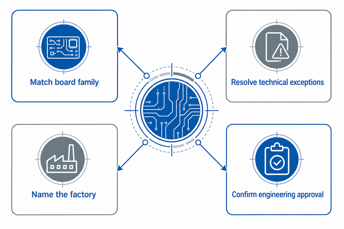
This comparison gives us a short list of suppliers that can discuss the same complete construction. Select suppliers within the board family and production route, and resolve technical exceptions prior to selecting a quotation. The manufacturer, factory and the approved process should be listed in the order so that future changes may be reviewed.
For a PCBark inquiry, send the fabrication data along with the released drawing via the engineering inquiry page, indicating quantity and the destination, as well as the required delivery date. If the project requires the fabrication and assembly scope to be defined, begin with the PCBark manufacturing and assembly overview. Prior to issuing the order, written engineering confirmation should finalize the open specifications.
References & Sources
Company profiles use suppliers’ public corporate and capability information, reviewed in September 2026. These statements are attribution based and aren’t factory audits. The following public technical references support the comparison method:
- NIST/SEMATECH: What Is Process Capability? Statistical distinction of stable process output from specification limits.
- IPC: Microvia reliability warning, March 2019. Historical evidence of latent failure after conventional acceptance.
- IPC Standards Revision Table. Base specifications and application specific addenda.
- IPC: Public release explanation for IPC-6012F. Rigid-board qualification scope and revision context.
- NASA: GSFC-STD-8001 revision A. GSFC mission-hardware scope, status and document date.
- NASA: Goddard center-specific standards register. Current listing context.
WHY WE WRITE THIS
About PCBark Engineering Insights
PCBark shares technical PCB fabrication and assembly guides based on real engineering review and manufacturing experience. We help teams compare materials, stackups, DFM risks, component sourcing, inspection plans, and production routes before they move from prototype to volume builds.
16+ yrs EMS experience
1-42 PCB layers
500,000 m2 annual PCB capacity
IPC Class 2/3 build discipline
DFM + test review