Get in touch with PCBark Company


Updated: July 2026. Reviewed by the Shenzhen Linghangda Technology Co., Ltd. (PCBark) technical team.
A 6 layer PCB is a printed circuit board built from six copper layers — four dedicated to signal routing and two dedicated to power and ground reference planes.
Quick Specs
| Layer count (core config) | 6 (4 signal + 2 plane) |
| Finished thickness | 1.6 mm (62 mil) standard; 0.8-2.0 mm alternates |
| Min trace / space | 3 mil (0.075 mm) standard |
| Min mechanical via | 0.15 mm (6 mil) |
| Impedance tolerance | ±10% standard, ±5% on request (TDR-verified) |
| Copper weight | 0.5-2 oz outer/inner typical |
| Prototype lead time | 48-72 hours typical (industry-standard range) |
In short: That extra plane pair over a standard 4-layer board gives four signal layers a solid ground layer or power layer to reference instead of one. It’s what cuts EMI and tightens impedance control — not the layer count itself. Whether you actually need it depends on pin count, interface speed, and power-rail count, not on how advanced your project sounds.
What a 6-Layer PCB Actually Buys You (Two Reference Planes, Not Just More Layers)
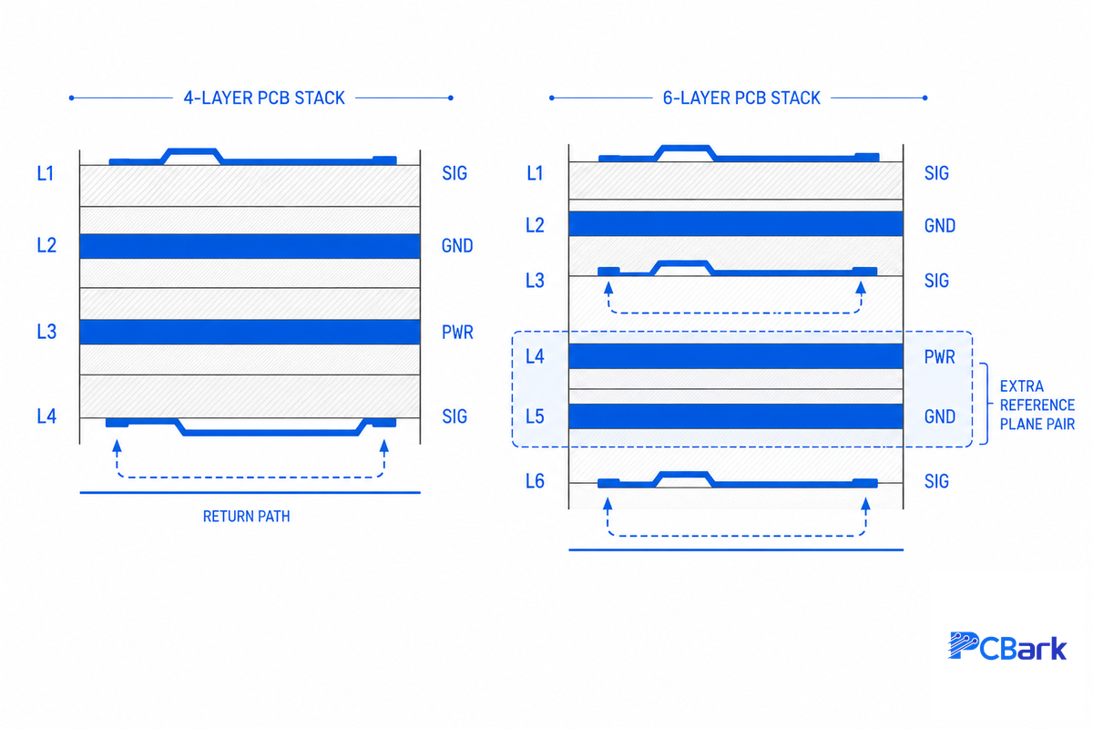
A 6-layer PCB is typically a printed circuit board manufactured with six copper layers – four of which are for routing signals and the other two for the power and ground reference – bonded together with insulation material between them. This is the same underlying construction discussed in our guide to 4-layer PCBs, but with an additional reference-plane pair. That second pair of planes, rather than the mere number of layers, is the critical difference because each signal layer is accompanied by a low-impedance return path immediately below it, which governs both impedance and radiated emissions.
It’s easy to assume that “more layers” equate to a more capable board, but that notion isn’t supported by evidence. In a LinkedIn post, PCB design consultant Vishnu Devasani starkly stated that the number of layers is “a design decision that balances performance, manufacturability, cost, and reliability… many people think more layers means better board.
Not always true.” An important distinction to understand before ordering any boards: not every layer in a nominally 6-layer board is used for carrying signals or power in all designs; some boards are created using a 6-layer process for cost or mechanical reasons, but some of those layers may not be routed heavily. The label on the fabrication drawing and the number of layers actively involved in electrical work aren’t necessarily the same.
Therefore, the straightforward explanation of what you gain with 6 layers is: two separate reference planes, sufficient space for four signal layers without compromising power distribution, and – with disciplined stackups and routing – the EMI benefits associated with an additional plane pair. If your design doesn’t require these benefits, opting for six layers is an expensive mistake that solves a problem you don’t have. The risk cuts the other way too: a board that genuinely needs the extra reference planes but gets built on a rushed 4-layer stackup instead tends to fail EMC compliance testing late, after tooling is already committed. PCBark’s DFM review catches that mismatch before fabrication, not after a failed test report — part of why the shop runs 100% electrical test and automated optical inspection on every inner core regardless of layer count.
When to Move From 4 to 6 Layers (and When 6 Isn’t Enough)

The time to consider a 6-layer PCB is when a specific, verifiable issue on your board can’t be resolved on four layers – not simply because you feel your project “deserves” more layers. The benefits of 6 layer construction are tangible, but they’re conditional and tied to particular electrical demands, not universal to all circuit board designs.
| Trigger Signal | Why 4 Layers Fails | Points To |
|---|---|---|
| High pin-count BGA (200+ pins) | Escape routing consumes both signal layers before fanout completes | 6 layers |
| 2+ high-speed interfaces (USB3, DDR, PCIe, multi-gig Ethernet) | Not enough dedicated, ground-referenced layers for controlled-impedance differential pairs | 6 layers |
| Mixed analog/digital domains on one board | No spare plane to physically separate domains while keeping both properly referenced | 6 layers |
| 3+ independent voltage rails, noise-sensitive | Single power plane forces rail-splitting compromises | 6 layers |
| Signals above 3 Gbps per lane with tight skew budgets | Fiber-weave-induced skew (see below) starts to dominate even a clean 6-layer stackup — may need laminate/routing changes, not just layers | 6 layers, possibly 8 or HDI |
| Wiring density persistently exceeds fab capability at reasonable size | Adding layers stops paying off before density is resolved | 8 layers or HDI with microvias, not more traditional layers |
If none of these apply, a well-designed 4-layer board will likely outperform a hastily assembled 6-layer one. A meticulously crafted 4-layer board with proper reference planes will frequently outperform a 6-layer board where extra layers were added as a work around rather than fixing a routing problem. Layer count is a symptomatic solution to specific electrical constraints, not a marker of engineering prowess.
💡 Pro Tip
Engineers on forums like r/PrintedCircuitBoard frequently debate the merits of different stackup configurations, such as SIG/GND/PWR/SIG/GND/SIG versus other power-adjacent alternatives, before confirming if six layers are even necessary. It’s best to resolve the layer count question using the table above before delving into layer order arrangements, which only become relevant once you’ve decided on a 6-layer board.
6-Layer Stackup Arrangements: The Arrangement Playbook
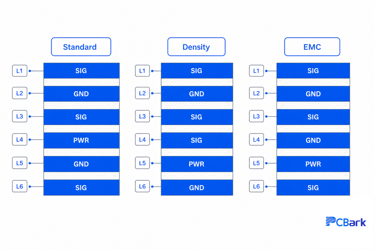
Once you’ve committed to a 6-layer PCB, the arrangement of those layers is a design choice rather than a default setting. Most real-world 6-layer designs fall into three primary configurations, each presenting a different trade-off between signal integrity, routing density, and RF isolation.
| Arrangement (L1-L6) | Reference Behavior | Best For | Watch Out For |
|---|---|---|---|
| SIG / GND / SIG / PWR / GND / SIG | Every signal layer sits next to a ground or power plane; PWR sandwiched between two GNDs | High-speed digital, mixed-signal boards — the industry-default “standard” stackup | A signal changing from L1 to L6 crosses from a GND to a PWR reference — needs a stitching cap near the transition |
| SIG / GND / SIG / SIG / PWR / GND | Two adjacent internal signal layers (L3/L4), maximizing routing channels | Dense BGA breakout where routing channels matter more than perfect SI | L3 and L4 share less shielding from each other — higher crosstalk risk between the two inner signal layers |
| SIG / GND / SIG / GND / PWR / SIG | An extra ground layer gives every signal layer (including the inner one) a dedicated GND reference | RF sections, GHz-class designs, EMC-critical boards | Costs you a signal layer versus the standard arrangement — routing channels shrink |
The arrangement choice isn’t academic. One documented case study of a Gigabit Ethernet switch board with DDR4 memory and multiple SerDes channels started on a TOP-SIG-GND-PWR-SIG-BOTTOM stackup and hit severe crosstalk between the two adjacent signal layers plus power noise disrupting SerDes performance; re-arranging to put a dedicated ground plane next to the top signal layer (TOP-GND-SIG-PWR-GND-BOTTOM) delivered a reported 40% signal integrity improvement and 6 dB more EMI test margin on the same board, same components, same layer count — arrangement alone, not layer count, was the fix. Academic work backs this up outside of vendor case studies too: a Georgia Institute of Technology ECTC 2024 paper on embedded multi-channel filters built directly into layers 3 and 5 of a 6-layer stackup treats the specific layer assignment, not just the total layer count, as the design variable that determines whether the filter actually works.
What the myriad of layer-order tables you find on the web won’t tell you is why the physical build-up of the dielectric layers matter just as much as the layer order itself. Typically, a 6-layer build is two thicker cores with a thin prepreg in between, or one thicker center core with thin outer prepregs, and the second is the much more defensible choice in most designs. Putting thin dielectric on the outer surfaces pull the power plane close to its neighbor ground, increasing interplane capacitance and reducing spreading inductance.
It also puts the inner signal layers close to their respective grounds and further from any gaps in the power plane, minimizing EMI and flattening the impedance near plane splits. Fab default stacks frequently put thin dielectric in the middle because it’s simpler to fabricate. If you’ve a lot of high-speed signals on a central layer with a large digital processor, don’t assume your fab’s standard will work; tell them specifically to use thin-outer-prepreg builds.
Whatever arrangement you settle on, program it into your PCB design tools before you start laying out the signals, not after. All the modern PCB design software-Altium, KiCad, Allegro-allow you to specify layer function and lock plane assignments in a stackup editor so that the impedance that you calculate matches the actual stack that gets built.
Search “6 layer pcb design guidelines” and you’ll find every fab publishes its own version of pcb stackup design guidelines in its design and manufacturing docs; use those as your first resource before building against assumptions rather than your actual fabricator’s capabilities. What a standard 6 layer pcb stackup looks like on paper and what your specific fabricator can actually build to are two different documents — confirm both before finalizing.
Typical 6-layer PCB stackup diagrams you’ll find in capability sheets are a starting point, not an endpoint. Stackup design isn’t only about layer order-board thickness, the base PCB material (e.g., high Tg FR-4, RF laminates), and the complexity of the design interact and influence each other. The single biggest cause of late-stage respins are isolated design or manufacturing decisions-picking a 6 layer PCB stack without verifying thickness and material choices with the fabrication house, even for “the” optimal 6-layer PCB stack-up.
Finish and copper weight on a finished board will matter more in the long run than the specifics of any one stackup diagram. If you’re weighing a 6 layer pcb vs 8 layer decision, the practitioner take below is worth reading before you commit either way.
“8 layers comes up when you have too many signals to fit in a 6 layer PCB and one of your layers is used for large power rails. I find this happens most often in designs with a large digital processor… you might also have a controlled impedance layer for a high-speed interface or a large number of I/Os, and that drives you into an 8-layer PCB.”
Controlled Impedance on a 6-Layer Board (Outer Microstrip + Inner Stripline)
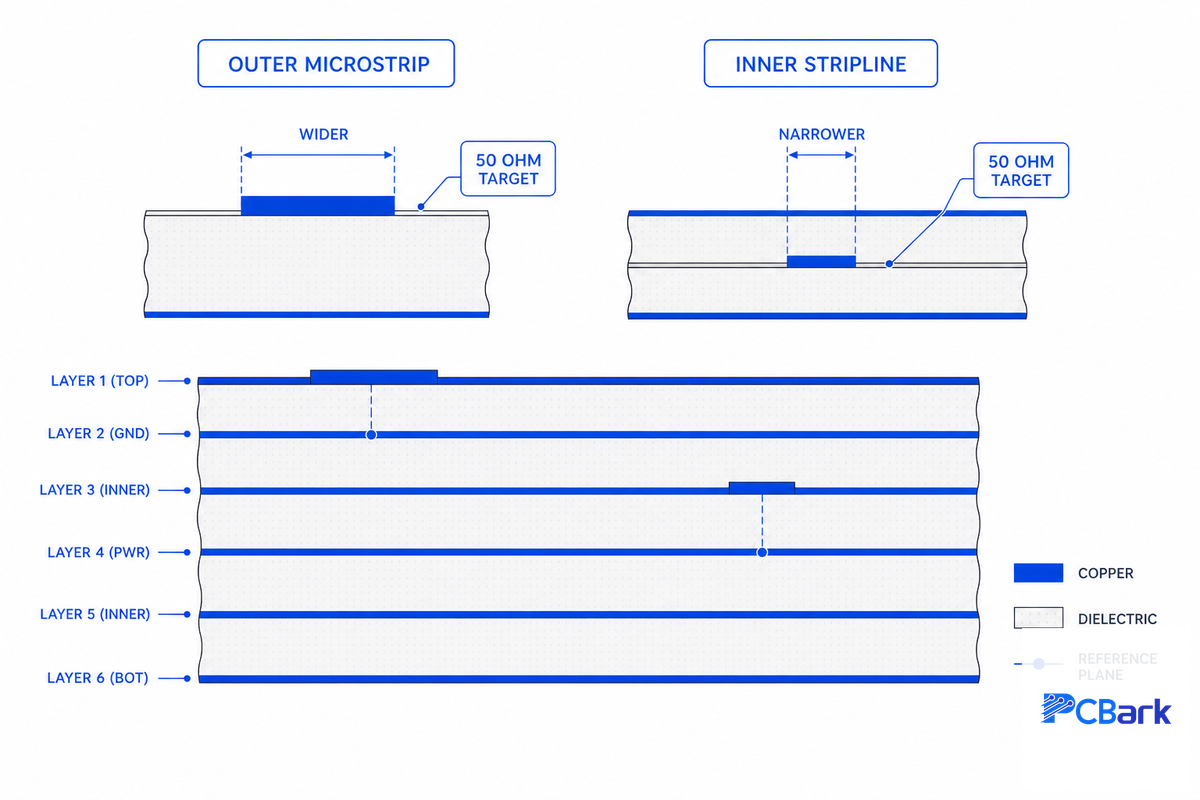
Control impedance is a 6 layer board design feature, not some ubiquitous blanket requirement — according to IPC’s controlled-impedance design standard, IPC-2141A, not all high speed digital and/or high frequency analog designs will have to pay any attention to this. However, if your board does have controlled impedance nets – any USB, Ethernet, DDR or RF front-end – then there’s some math that you do have to get right, and that’s different from outer layer math versus inner layer math.
📐 Engineering Note — worked example
Let’s assume a basic 6-layer board with FR-4 dielectric, Dk=4.1-4.2, and the dielectric thickness to the next ground plane is 7 mils – this geometry isn’t sacred (both Dk and thickness impact the result), but for a 50-Ohm single-ended trace on the top surface layer (microstrip), it yields about 13 mils. (It can be independently verified in a bunch of RF-PCB curriculum RF-PCB microstrip calculator (e.g. Harvey Mudd’s and various fab vendors’) tools for that stack up).
Take that same 50 trace and move it to an inner signal layer as a stripline (sandwiched between two reference planes, rather than exposed on one side). That trace need to be much narrower – the second reference plane couples to the signal from both sides, and matching that same impedance figure requires between one third and half of the outer layer trace width, depending on the thickness of the dielectric on each side. None of the top competitive guides on this keyword calculate that inner layer impedance, they just cite the outer layer impedance figure and say the inner layers just “have to be narrower.”
There are two honesty notes in here, and both of these come from the Provenance Level discipline, not the optimism. First, a trade-journal stackup analysis (PCD&F) designed for a specific six-layer stackup having both outer microstrip and inner stripline traces actually determined that the outer layer copper has greater post-plating width variation than the inner layer copper – the inverse of the normal assumption that the outer layers are easier to hold tight. Second, the same analysis points out that analytical impedance formulas generally are only accurate to around 10% and without a full field-solver, that number need to be treated as a discussion starter for the fabricator rather than an immutable number to present for a purchase order, ask for your fabricator’s coupon-verified stackup and TDR report prior to placing.
There’s one trickier edge case to watch for if your lanes are going beyond about 3 Gbps: Some research out of Auburn University’s signal-integrity program regarding transmission lines in anisotropic PCB dielectrics (like most of today’s common FR-4 laminates) shows that the periodicity of the fiber weave on the PCB’s internal dielectrics can lead to significant differential-pair skew, above that data rate, in a way that the simple microstrip/stripline width math described above (which assumes a uniform dielectric) entirely misses. If you’re at that speed tier, talk to your fabricator about fiber-weave-aware laminates or ask about routing the critical differential pairs at a slight angle to the glass weave. These signal integrity requirements are where design quickly start differentiating between ordinary and advanced PCB projects-after about 3 Gbps, signal- and power-integrity math quickly start diverging, although they’re otherwise largely identical up to that point. Getting the impedance target wrong isn’t a cosmetic problem — it’s a hidden risk that only shows up as an intermittent failure in the field, which is why PCBark issues a TDR verification report on every controlled-impedance order instead of relying on the calculator alone.
Return-Path Routing, EMI Control & Power Delivery: The 6-Layer Return-Path Field Manual
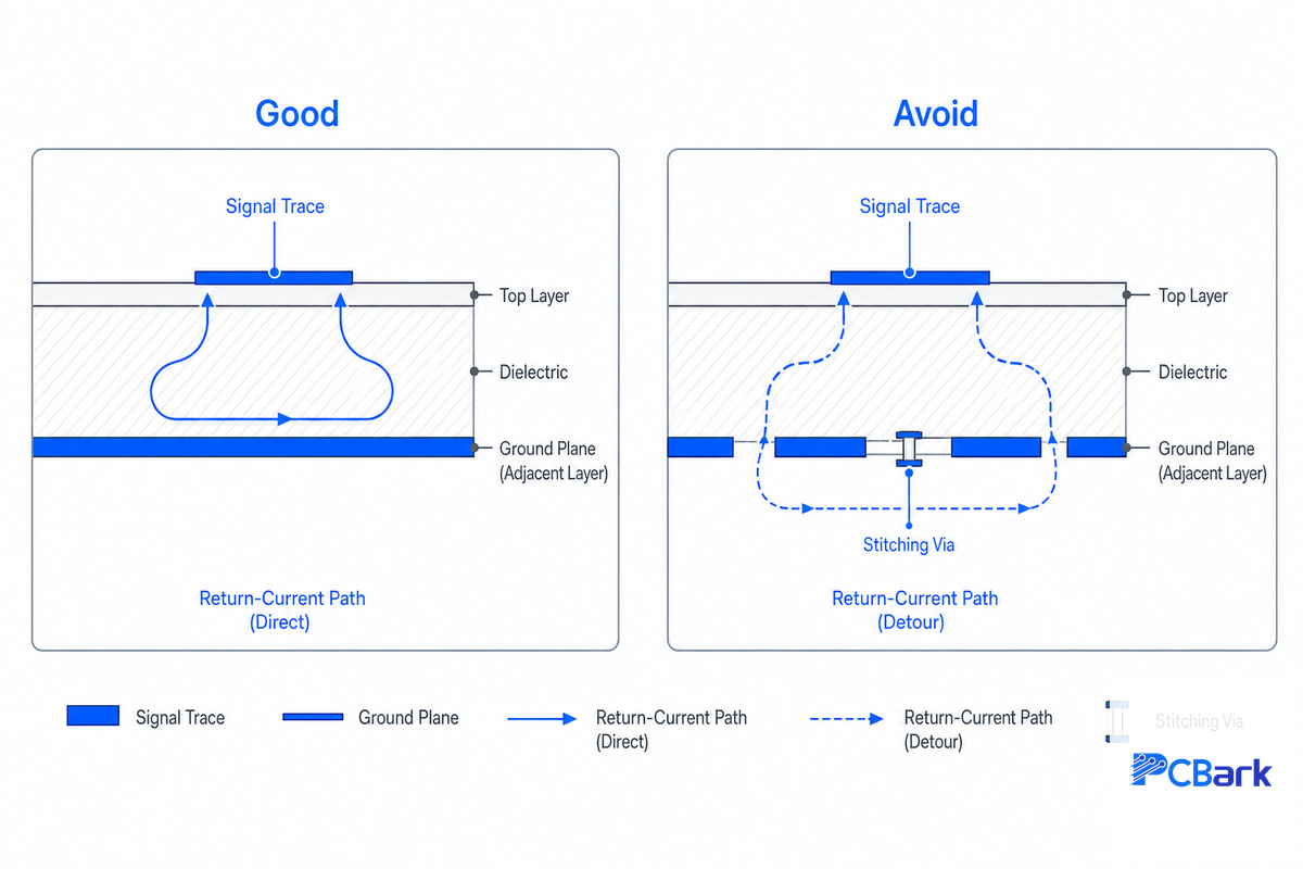
Most signal integrity problems on six-layer PCBs trace back to one question: where is the return current actually going? Having two pairs of reference planes instead of one provides you with many options for where the return current can go-and plenty of ways to break it without ever knowing.
- ✔ Every high-speed trace run over an unbroken plane for its entire length, no gaps, no splits.
- ✔ Where a trace must cross a plane gap, a stitching capacitor sit within a few millimeters of the crossing.
- ✔ Every signal via that changes layers has an adjacent ground return via, so the return current isn’t forced to hunt for a path through a different plane.
- ✔ Ground stitching vias around the board perimeter and near connectors, used for EMI containment (not to be confused with waveguide-style via-fencing for cavity isolation, which follows different spacing math), are spaced at λ/20 or tighter for low-frequency designs, λ/10 for high-frequency circuits (λ = wavelength of the highest frequency of concern) — a rule independently confirmed across multiple PCB engineering references, not a single vendor’s house number.
One habit persists in older PCB layout guidance and needs to be retired: splitting the ground plane to separate “analog” and “digital” sections. It reads as a clean, deliberate decision, but any signal that has to cross that split, an ADC input line, for instance, forces its return current into a long detour, which radiates and couples into neighboring nets. EE Times’ analysis of radiated EMI through PCB stack-up design and Cadence’s layer-stackup guidance both converge on the same fix: keep one unbroken ground plane and separate domains by component placement, not by cutting copper. One patent filing for a real biosignal-acquisition device documents exactly this discipline in production: a 6-layer board laid out with split analog/digital/supply-ground planes plus via stitching and explicit return-current optimization, precisely the practice this section describes.
For 6 layers, we apply the same two-plane-pair thinking for power. Your power-ground plane pair acts as a distributed capacitor through the dielectric separating the planes; use a thin dielectric between these (often less than 0.1 mm to maximize interplane capacitance) to shift the useful decoupling range to higher frequencies where you won’t be as dependent on your ceramics. Put 0.1 µF and 1 µF decoupling capacitors on all ICs connected to both plane pairs (not just one), and if you’ve high-current portions of the board, you know the extra plane pair provides a second option for thermal management via thermal vias beyond just decoupling – on a 4 layer board, you would often be stuck making a compromise between decoupling and heat-sharing for that single pair of planes.
And the last thing before sending out the completed board design is to run a design rule check on the real stack-up that you chose, not on the net list that your schematic used. Did all your high-speed nets end up referenced to solid plane, did all plane transitions have adequate clearance, did your impedance to net widths match your real dielectric thickness. Here’s where your power integrity and your return-path integrity are tested as a pair, rather than two bolted-on DRC checks done last minute.
Those additional routing layers on a 6-layer board are only beneficial if that final review is done. Otherwise they’re a wasted cost.
Via Strategy: The 6-Layer Via Compatibility Index
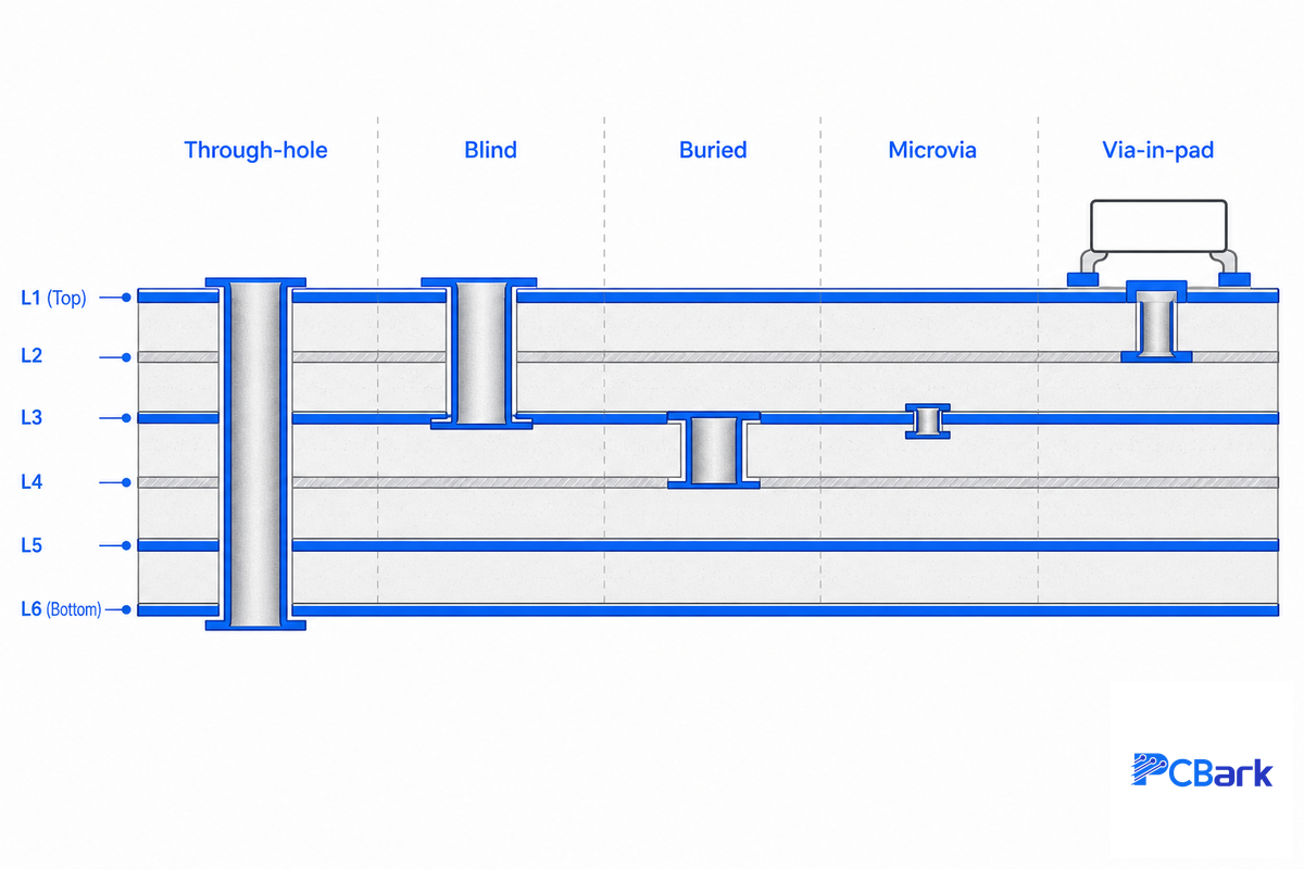
Though IPC-4761, a design guide, actually refers to the protection methods of the vias and the underlying production/material trades offs, rather than providing a definite compatibility table, it’s the correct place to determine what your vias actually are going to cost you in terms of lamination cycles.
| Via Type | Connects | Lamination Impact | Use It When |
|---|---|---|---|
| Through-hole (plated) | All 6 layers, top to bottom | Single cycle — cheapest | Default for most 6-layer boards |
| Blind | Outer layer to one inner layer | Adds a lamination cycle | Escape routing under fine-pitch BGAs |
| Buried | Two inner layers only | Adds a lamination cycle | Freeing outer-layer routing space |
| Microvia (laser) | Adjacent layers, ~100 µm drill | Sequential HDI build | HDI-hybrid 6-layer, ≤6 mil features |
| Via-in-pad | Component pad to inner layer | Needs filling + capping/plating over | Fine-pitch BGA fan-out where space is tight |
| Thermal via | Component pad to a plane | Single cycle | Spreading heat under power parts |
| Stitching via | Ground plane to ground plane | Single cycle | λ/20-λ/10 perimeter EMI containment |
| Return via | Beside a signal via, to the plane | Single cycle | Every high-speed layer change |
| Tented / plugged | Any via, sealed per IPC-4761 | Finish step, no extra cycle | Protecting vias near or in pads |
And the lamination-cycle column there, the one that actually determines your quote, is where reliability risk lurks. A frequently-cited University of Maryland (CALCE) reliability study of copper-filled stacked microvias (independent academic research, not a PCBark finding) points to the same conclusion: it isn’t the presence of a void itself, but voiding during the fill process that drives failure. That study’s headline figure — a 16% conical void in a filled microvia reduces the fatigue life to a paltry 1.4% of that of a void-free via — is one third parties in the industry still reference as a rough benchmark for void acceptability, though it comes from a single academic source rather than a broad industry survey.
That’s not just an anomaly; that’s the difference between passing and failing a thermal-cycling test. If your layout utilizes a via-in-pad configuration or stacked microvias for a compact BGA, press your fabricator for some form of void-detection (cross-section or X-ray) instead of simply listing “via-in-pad” on the drawing.
What Really Drives 6-Layer Cost: The Cost-Lever Cascade

Layer count is only part of what sets 6-layer PCB price. As IPC-2141A’s design-for-manufacturing framework defines it, cost tracks fabrication complexity — inner-layer imaging, lamination cycles, drill holes, plating, and outer-layer processing — not the layer count on its own. That lamination-cycle sensitivity is well-documented outside marketing copy too: one granted patent on PCB lamination optimization methods exists specifically because reducing lamination cycles for a given layer count is valuable enough engineering IP to protect.
| Cost Lever | Impact |
|---|---|
| Blind / buried vias (sequential lamination) | Largest — each extra lamination cycle is a step change, not a marginal add |
| Impedance tolerance tier | Significant — a ±5% tolerance costs more to hold than ±10%, which costs more than ±15% (confirmed cost ordering, not just “tighter = pricier”) |
| Copper weight / exotic laminate (Rogers, high-Tg) | Moderate — material and process cost, scales with material choice |
| The two extra layers themselves (single-lamination, standard tolerance) | Smallest of the four — a disciplined single-cycle 6-layer build sits closer to 4-layer pricing than to a blind/buried build |
You’ll see any headline figure thrown out – a step of something around 30-40% from 4-6 layers – and the headline is right in terms of the order of magnitude but it’s not a hard number. We’ve seen one detailed prototype-to-production cost breakdown where the premium is actually some where between 50-65% at small prototype sizes, falling down to something more like 50-60% at production volumes depending on board size (others cite closer to 30-40%). Both estimates are right – the honest answer is the premium depend on board size, volume tier, and which of the levers below you push much more than a fixed, universal percentage.
Cost control should follow from the ranking above – avoid blindly applying blind/buried vias unless your routing absolutely requires them for escape, use an evenly weighted layer stack-up (uneven copper distribution causes warping when reflow soldering), specify only the impedance tolerance required for the signals, and consult your board fab before you get your final design for quote rather than after the price shock hit you.
Beyond the stack-up and material choices, 6 layer pcb fabrication is its own manufacturing process for turning that design into actual boards, whether you need a full pcb 6 layer run or a smaller prototype batch first: early confirmation of the thickness of a 6-layer PCB and its material combination (which determines impedance and warp) are essential, and any custom PCB requirements outside the standard set from your fab should be treated as a lead-time add regardless of layer count. Always ask for separate 6-layer PCB prototype and production pricing because they’re on different cost curves and any quote that shows only one level can’t be assessed for overall value. You can also be pretty confident the fabricator is worth working with if they proactively call out pcb manufacturing and assembly constraints (component keep-outs, pcb surface finish, clearances on assembly sides, etc) during DFM rather than waiting until the first piece of hardware comes back and fails the final inspection — that discipline is a stronger signal than any marketing claim about being the best 6-layer PCB option on paper.
And if you continually find yourself trying to stuff ever-increasing wiring densities into a traditional 6-layer stack-up, that’s often a sign you should be considering a higher-density fabrication technology instead of trying to stuff ever more layers in.
Industry Outlook: What’s Actually Changing for 6-Layer Boards

In reality, today’s layer count growth across the PCB industry isn’t driven by anything remotely approaching a mainstream 6-layer board.
Vexos noted in a recent OEM supply chain study that the number of layers on the average AI server PCB is projected to jump from 18 in 2023 to 32 in 2025 (a ~78% jump in 2 years – although this is from a single-source trend estimate, not an industry-wide count). And the increase in the layers is being driven by factors such as the I/O density and power requirements of AI accelerator chips – nothing that comes up on a standard industrial control board or networking product. From our keyword research trends data we see that the searches for “6 layer pcb” remained largely stable through 2026 while searches for “multilayer pcb” in the aggregate went through a major spike and subsequent correction late in 2025 – indicating that six-layer boards are largely outside of the current period of volatility.
Market intelligence provides a helpful caveat: As of 2025, the total PCB market is growing unevenly, with a large chunk of the sales increases going to suppliers targeting AI/data-center needs with high-layer-count and HDI products, and most suppliers seeing less than 10% sales growth even in a strong year, according to industry analyst Prismark. When read together, this indicates that anyone spec’ing a 6-layer board in 2026 won’t be chasing a moving target: The stackup logic, technology, and cost structure detailed in this guide represent stable, mature solutions, with “growth” news focusing on a higher-layer-count market. This stability can be valuable information for program planning for 2026-2027, as a 6-layer spec finalized today should remain relevant, unlike a bleeding-edge HDI spec.
For context, only the overall market size: Global market for multilayer PCBsis around $81-$87 billion in 2025, with conventional forecasts calling for CAGR of 5-6% to the early 2030s; these are directional numbers for the market as a whole, not for 6-layer boards in particular.
FAQ: Frequently Asked 6-Layer PCB Questions
Q: What does “6 layer PCB” mean?
View Answer
A 6-layer PCB is one built up from six alternating layers of copper and insulating dielectric material, with the standard stackup featuring four signal layers and two planes – one power and one ground. It is that second set of planes that gives each signal layer a reference plane close enough to reduce EMI and enable more controlled impedance.
Q: What is the difference between a 4-layer and a 6-layer PCB?
View Answer
Compare this to a 4-layer board, which has two signal layers and one set of planes (power and ground). A 6-layer board provides two extra signal layers (more routing density) and another pair of reference planes (better EMI performance and controlled impedance) and usually costs 30-65% more than a 4-layer board of the same size and volume.
Q: How thick is a 6-layer PCB?
View Answer
6-layer PCB thickness for most standard 6-layer PCBs is manufactured at 1.6mm (0.062 inches) — a common 6-layer PCB stackup 1.6 mm reference point you’ll see quoted across fabricator capability sheets — but 0.8, 1.0, 1.2, and 2.0 mm boards are also available for use in high-power, high-density, or space-constrained applications. Thinner boards can some times cost more than 1.6mm due to increased processing difficulties and higher scrap rates. Always consult your board fabricator for their capabilities and ensure that connector and enclosure tolerances match your PCB thickness.
Q: What is the minimum trace width and spacing for 6-layer PCBs?
View Answer
Most 6-layer fabrications are capable of a 3- to 4-mil (0.075-0.1mm) trace width and spacing, with 2-mil capabilities readily available through hdi-hybrid designs utilizing laser microvias. It’s worth noting that controlled-impedance nets are usually significantly wider than the minimum. A 50 Ohm outer layer microstrip, for instance, will likely end up around 13 mils depending on the dielectric stack; the 50 Ohm inner stripline layers will need to be substantially narrower. You should always refer to your board fabricator’s coupon-verified stackup when calculating traces for impedance.
Q: Is a via teardrop necessary on 6-layer boards?
View Answer
While not needed on every via, this practice can offer inexpensive insurance against fatigue failure in a few critical applications, such as where rigid and flexible boards connect, designs experiencing high levels of vibration, and any high-layer-count design where tolerances start to add up with the drill depth. Teardrops reduce stress concentrations at the junction of a trace and via pad, thereby minimizing one type of failure mode.
Q: Do I need a dedicated power plane, or can I reference ground only on layer 3?
View Answer
It really comes down to how many rails and how noisy your environment is. For simple low-current designs, a single shared ground plane with power as a copper pour on signal planes is fine and gives you one more plane back to work with. Any design that has more than one independent power level or just high currents that need to be distributed low-impedance should pay the price for having dedicated ground plane tightly associated with a dedicated power plane which doubles as a de facto decoupling capacitor where a thinner dielectric is the best value.
Q: Standard vs. “pseudo” 6-layer PCB, which should I specify?
View Answer
Typical 6-Layer: Our most common six-layer PCB stackup configuration is 6-layer FR-4 fully laminated continuous copper six layer PCBs with thru-hole vias. This the less expensive, more manufacturable, and generally preferred choice as a default configuration for most PCB design requirements, since you achieve reliable signal performance without adding the complexity and expense of a build with blind or buried structures. Pseudo/Hybrid 6-Layer: With a pseudo- or hybrid-6 layer PCB design you introduce some level of blind or buried vias, or HDI style sub-build to layers, in an effort to wring out higher performance for very fast signals or better crosstalk performance, but with additional cost and a longer lead time.
Use this version only when one of your technical requirements, like a specific data rate, a very strict crosstalk budget, or a routing challenge, simply can’t be satisfied by our standard6-layer build; don’t default to it simply because you can. For the vast majority of6-layer pcb design projects, a 6-layer stackup is the first and only option.
About This Engineering Guide
This is an aggregate data sheet covering 6 layer PCB stackup, impedance, via, and costs from the IPC standards, University signal-integrity research, as well as identified Industry leaders – the results are compared and contrasted with PCBark’s own in-house impedance-controlled fabrication – 100% electrical test, automated inspection on all inner cores, X-ray on BGA, and section/micro-section – available for 5+ years per lot. When data from sources didn’t agree – we demonstrate the variance and its reason – instead of just choosing a number to appear omniscient. Validated by PCBark technical.
Building a 6-Layer PCB?
PCBark fabricates 6-layer boards to a published ±10% impedance tolerance (±5% on request) with a TDR report on every controlled-impedance order, plus 100% electrical test, automated optical inspection, and X-ray on BGA joints — the kind of traceability that separates a high-quality 6-layer PCB manufacturer from a commodity prototype shop. See PCBark’s 6-layer PCB manufacturing capabilities for stackup options, capacity, and a same-day DFM review, or explore the full multilayer PCB range from 4 to 42+ layers.
References & Sources
- IPC-2141A, Controlled Impedance Design GuideIPC (Association Connecting Electronics Industries)
- IPC-4761, Design Guide for Protection of Printed Board ViasIPC
- Signal Integrity Analysis of Transmission Lines in Anisotropic PCB DielectricsAuburn University (S. Peddada thesis)
- Reliability of Copper-Filled Stacked Microvias in High Density InterconnectsUniversity of Maryland (CALCE)
- A Multi-Channel, Embedded, and Geometrically Optimized FilterGeorgia Institute of Technology, ECTC 2024
- GSFC-STD-8001, Standard Quality Assurance Requirements for Printed Circuit BoardsNASA Goddard Space Flight Center
- Controlling Radiated EMI Through PCB Stack-upEE Times
- Design PCBs for EMI, Part 2: Basic Stack-upKenneth Wyatt, EDN
Related Articles
- 4 Layer PCB Design Guidethe single-plane-pair baseline this guide builds on
- Multilayer Flex PCB Design Guidewhen your 6-layer design needs to bend
- Industrial Control PCB Guideruggedization and temperature grading for harsh-environment boards
- HDI vs Multilayer PCBwhen microvias beat adding another conventional layer
- Multilayer PCB Manufacturingthe full 4-to-42+ layer range