Get in touch with PCBark Company
Equipment limits outrank marketing claims for high-aspect-ratio holes and fine traces
Schmoll + Tongtai CNC drills (~24) and Newway LDI in-house.
Ask: name the drill and imaging machines and their max aspect ratio.

PCBark is engineered for 32-to-42-layer printed circuit board constructions, a documented process capability into the 32+ layer tier that few commercial fabs publish in verifiable spec form. Built for HPC and AI servers, 400G/800G telecom backplanes, aerospace and defense backbones, and advanced medical and test systems. This is the high end of the multilayer PCB design ladder, a long way past double-sided PCBs and the simpler 2 to 32 layers most shops handle.
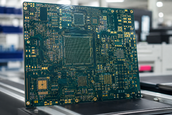
Push a board past 30 layers and yield falls off a cliff, industry experience flags a clear “>30-layer yield drop” where a single 25µm misregistration shorts or opens a net, and every added cycle multiplies the cost of a scrapped panel. That’s the real reason this tier intimidates buyers, and the reason more layers don’t make a board better. Extra layers give the routing and the reference planes room to behave, a bad stack-up on six layers still behaves badly regardless of the number of layers.
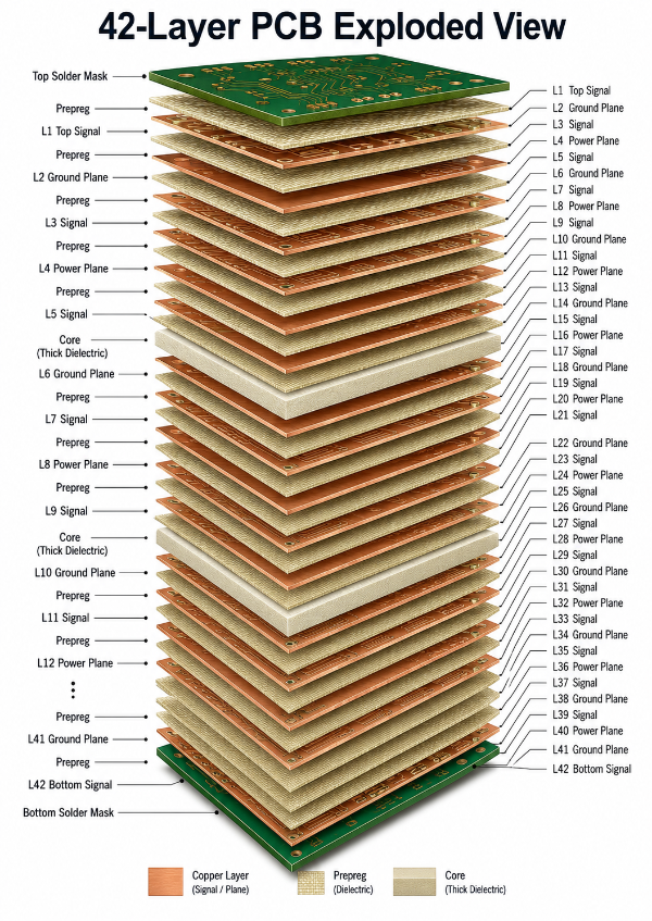
A 32–42 layer construction earns its cost only when pin count, interface count, and power-domain complexity physically exceed what 16–24 layers can route with clean return paths. That’s the honest frame for this tier. In pcb stack-up design terms, the complex designs below genuinely need these PCB layers; many that ask for them actually need a right-sized 24-layer stack-up with disciplined plane assignment. Where the design driver is real, 32–42 layers becomes the difference between a manufacturable board and a respin, and these aren’t ordinary circuit boards.
| Design driver | What it forces | Why 32–42 layers helps |
|---|---|---|
| 1,500+ pin BGA fan-out | Escape routing on many signal layers | Dedicated routing layers between plane pairs keep escape traces short and impedance-controlled |
| PCIe 5.0 / DDR5 / 400G–800G interfaces | Many controlled-impedance differential pairs | Tightly coupled stripline pairs with adjacent ground planes for return-current continuity |
| Complex power delivery (many rails) | Multiple low-impedance power planes | Separate power and ground plane sets reduce IR drop and plane resonance |
| EMI / crosstalk containment | Shield layers around aggressors | Plane shielding between high-speed groups suppresses radiated EMI and crosstalk |
| Extreme interconnect density | Blind/buried vias to free up real estate | Layer pairs joined by buried vias recover routing channels lost to through-holes |
| Layer tier | Typical application | Typical material | What this tier is for |
|---|---|---|---|
| 2–4L | Consumer, IoT, simple control | FR-4 | Cost-driven volume electronics |
| 6–8L | Industrial control, basic embedded | FR-4 / High-Tg FR-4 | Adds one plane pair for cleaner power/ground |
| 10–16L | Networking line cards, automotive ECUs | High-Tg, halogen-free | Multiple high-speed buses with isolation |
| 18–24L | Servers, switches, medical imaging | High-speed laminate | Dense BGA fan-out + many differential pairs |
| 32–42L | HPC/AI server backplanes, 400G–800G telecom, aerospace backbones | Rogers, Isola, Panasonic Megtron, hybrid | Commercial-production ultra-high-layer tier — PCBark’s documented range |
| 50–64L | Specialized test, core-router backplanes | Low-loss hybrid stacks | Niche ultra-density, low-volume |
| 108L | Long-standing semiconductor-test ceiling | Exotic low-loss | R&D / wafer-test fixtures |
| 124L | OKI 124-layer record (2025), HBM/AI wafer test, 7.6mm thickness | Exotic low-loss | Industry-ceiling landscape, not commercial production |
| 129L | Denso 2012 theoretical record | Research | Reference ceiling only |
Positioning is the takeaway here, not bragging rights. The industry sat at a ceiling of 108 layers until OKI reached 124 layers in 2025 , and that 124 layer pcb exists for AI semiconductor wafer-test fixtures, not for shipping in a product. PCBark’s 32–42 layer tier sits where commercial high layer count pcb production actually happens, high enough to route the densest high-density AI and telecom designs for industries like aerospace, grounded enough to fabricate at yield. This is advanced pcb work where electromagnetic interference between high-speed groups has to be contained by plane shielding, not wished away. For broader layer-count selection, see the multilayer PCB hub, or step down to the 16–24 layer page when the design driver doesn’t justify this tier.
“Adding layers does not rescue a marginal stackup. We see designs land at 36 layers that route cleanly at 24 once the plane assignment and via strategy are right-sized. Layer count should follow the return-path and density requirement, never the other way around.”
This is the table buyers actually need: the measured process capability for the 32+ layer tier, not a banner. Every value below comes from PCBark’s documented capability sheet for the Maximum (32L+) column. Read it the way you would read a coupon report, these are the limits the line is built to hold for a 32 layer pcb through a 42 layer pcb construction, where impedance control and process control decide whether the board yields.
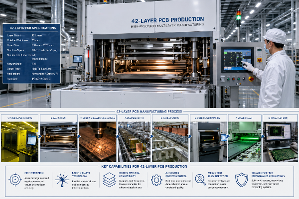
Two numbers carry the credibility of this tier: registration and hole copper. PCBark documents ±35µm layer-to-layer registration. Industry sources put the registration baseline for 50-plus-layer boards near ±5 mil (0.127 mm) , which makes the documented ±35µm roughly 3.6× tighter than that commonly cited baseline, and a typical accepted layer-to-layer figure of ≤50µm is also bettered. On hole copper, IPC-6012 Class 3 requires an average plated barrel of ≥25µm (1.0 mil) ; the documented ≥35µm sits above that Class 3 minimum. These margins are why a high-layer build survives thermal cycling and rework instead of cracking a barrel on the fourth lamination pass.
Pick the tier your design actually needs. This matrix uses real parameter values across the three capability bands, so a 24-layer board doesn’t get charged for a 42-layer process, and a true high-layer design lands in the tier built to hold its tolerances.
| Parameter | Standard (4–12L) | Best (14–24L) | Maximum (32L+) |
|---|---|---|---|
| Min trace/space | 0.10 / 0.10 mm | 0.075 / 0.075 mm | 0.050 / 0.050 mm |
| Hole copper | ≥20 µm | ≥25 µm | ≥35 µm |
| Impedance tolerance | ±10% | ±8% | ±5% |
| Registration | ±75 µm | ±50 µm | ±35 µm |
| Bow & twist | ≤0.75% | ≤0.50% | ≤0.30% |
| BGA pitch | 0.50 mm | 0.40 mm | 0.30 mm |
| Max board size | 400×500 mm | 500×600 mm | 600×1200 mm |
| Surface finish | HASL-LF, OSP, ENIG | ENIG, ENEPIG, Imm Ag | ENEPIG, hard gold |
High layer counts at multi-gigabit data rates push material selection toward low-loss laminate, a trend documented in low-loss thin-dielectric patent research. PCBark’s Maximum tier supports High-Tg FR-4, halogen-free systems, and low-loss families including Rogers, Isola, and Panasonic Megtron, plus hybrid stacks that pair a low-loss dielectric on the high-speed signal layers with FR-4 elsewhere to manage cost. High-Tg boards also hold up better to abuse, rework, and repeated solder reflow a quiet reliability factor that matters once a 32–42 layer board reaches PCB assembly. Material, dielectric constant, and dielectric thickness are part of the impedance solve, not an afterthought; send the target impedance with your stack-up and the front-end CAM team will close it against the chosen insulating material once the cores are laminated together. Solder mask and silkscreen color and finish are confirmed at the same stage from your pcb design file and Gerber files.
A real 40-layer board isn’t 40 layers stacked with through-vias. Buyers read a through-via-only high-layer board as low value, and they’re right to: the routing density and signal integrity that justify this tier come from sequential lamination plus blind and buried vias, not from drilling one deep stack of holes. Multilayer pcb manufacturing at this tier is a different process from building ordinary multilayer printed circuit boards, and understanding the manufacturing process is what tells a real fab apart from a banner. Below is how PCBark fabricates the 32–42 layer range, equipment named so you can verify it during the design phase.
40-layer through-via builds waste routing channels and stub signal lines, hurting density and signal integrity.
Long through-vias block inner-layer routing and leave stubs that degrade high-speed differential pairs.
Sequential lamination with blind, buried, and stacked vias recovers routing layers and shortens via paths.
In-house Schmoll/Tongtai drilling, Newway LDI imaging, and metallographic microsection QA on every high-layer lot.
This named sequence maps each process step to the actual machine that runs it and the quality gate that signs it off. A 32–42 layer board is fabricated as a set of inner-layer “books,” each built on a core board, that are bonded and laminated together in 4–6 sequential lamination cycles, with blind and buried vias drilled, plated, and copper-filled between cycles. High aspect ratio in these constructions, a thick board with small holes, is exactly why drill rigidity and laser direct imaging precision decide whether the board yields — and why high-density layer counts push toward laser-drilled blind and buried vias, as described in laser via-formation patent literature.
Sequential lamination subjects the inner books to several passes above 260°C. Patent literature is blunt about the failure mode: repeated high-temperature pressing can accelerate via failures and cause “circuit swimming,” where conductor and dielectric drift apart. That’s why this tier needs low-loss prepreg and dielectric systems with high Tg and high modulus to resist registration drift across cycles, and why blind/buried via formation between cycles, rather than one deep through-via stack, keeps aspect ratio and plating within reach. Via-in-pad with copper fill supports fine-pitch BGA escape; back-drill removes through-via stubs that would otherwise corrupt high-speed signals above 25 Gbps.
Terminology here isn’t decoration. Microvias, blind vias, buried vias, via-in-pad, laser direct imaging, controlled impedance, differential pairs, crosstalk control, low-loss dielectric, back-drill, aspect ratio, prepreg, and dielectric selection are the actual levers a 32–42 layer build turns. These are the levers design engineers and our own process control turn to keep manufacturability inside reach on complex designs. For the design-side view, see our stack-up design guidance in PCB layer stackup design and the via taxonomy in microvia, blind & buried vias.
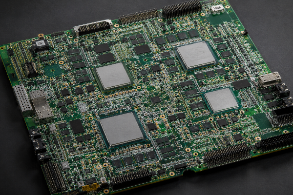
Competitors leave this section out. Sourcing a high-layer board is hardest at the step of separating polished marketing promises from actual verified capability and one real buyer put the cost of getting it wrong plainly: “the through-hole plating was no good, my first purchase was my last purchase. Didn’t end up saving money, only lost money.” Seasoned sourcing advice is blunt about how to avoid that: “Actual equipment capabilities outrank polished marketing claims” , so verify specific machinery limits and demand references. And: “Ask for IPC-6013 test coupons, microsection reports, and electrical-test records for representative production lots” .
Below is a type-clustering checklist that operationalizes exactly that, run it against any professional pcb supplier, including us, before board production starts.
Equipment limits outrank marketing claims for high-aspect-ratio holes and fine traces
Schmoll + Tongtai CNC drills (~24) and Newway LDI in-house.
Ask: name the drill and imaging machines and their max aspect ratio.
Cross-sections reveal registration, bond lines, and barrel quality you cannot see from outside
Metallographic microsection per IPC-6012/6013 on high-layer lots.
Ask: request a microsection coupon report for a representative lot.
Confirms controlled impedance was actually achieved, not just specified
TDR impedance test with Type Z coupons.
Ask: request the TDR coupon data with the tolerance window.
Thin barrels crack under thermal cycling — the classic high-layer field failure
Documented ≥35µm, above IPC-6012 Class 3 minimum.
Ask: request plated hole-copper measurements.
Sequential lamination compounds registration error across cycles
±35µm documented + registration coupon per lot.
Ask: request the registration coupon result.
First-pass yield on high-layer work is the real-world capability signal
Front-end CAM/DFM review before build to protect yield.
Ask: request typical first-pass yield and reference customers.
Class 2 vs Class 3 defines acceptable voids, fill, and annular ring
Boards built to IPC-A-600 / IPC-6012 Class 2 or 3 as specified.
Ask: confirm the IPC class and acceptance standard in writing.
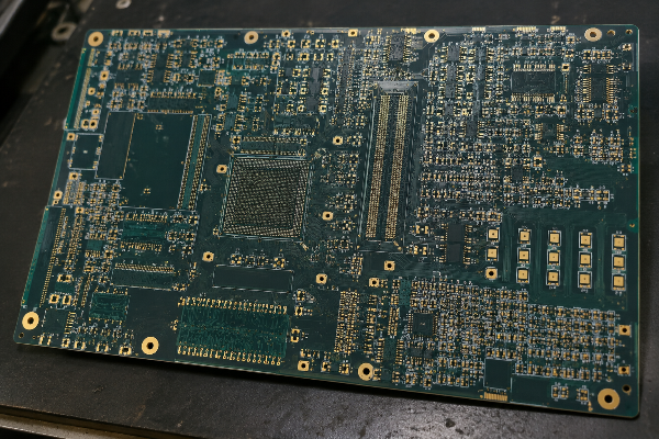
Run those seven asks on every quote and the field narrows fast. A fab that ships a microsection coupon, TDR data, registration results, and an IPC class statement is demonstrating verified capability; a fab that answers with adjectives is selling a banner. How these PCB test coupons are built and read is itself documented industry practice. Because the sequential nature of high-layer fabrication compounds registration error at every step, coupon evidence isn’t paperwork, it’s the only honest way to confirm a 32–42 layer board was built to tolerance, and the same standard PCBark applies before a high-layer lot ships.
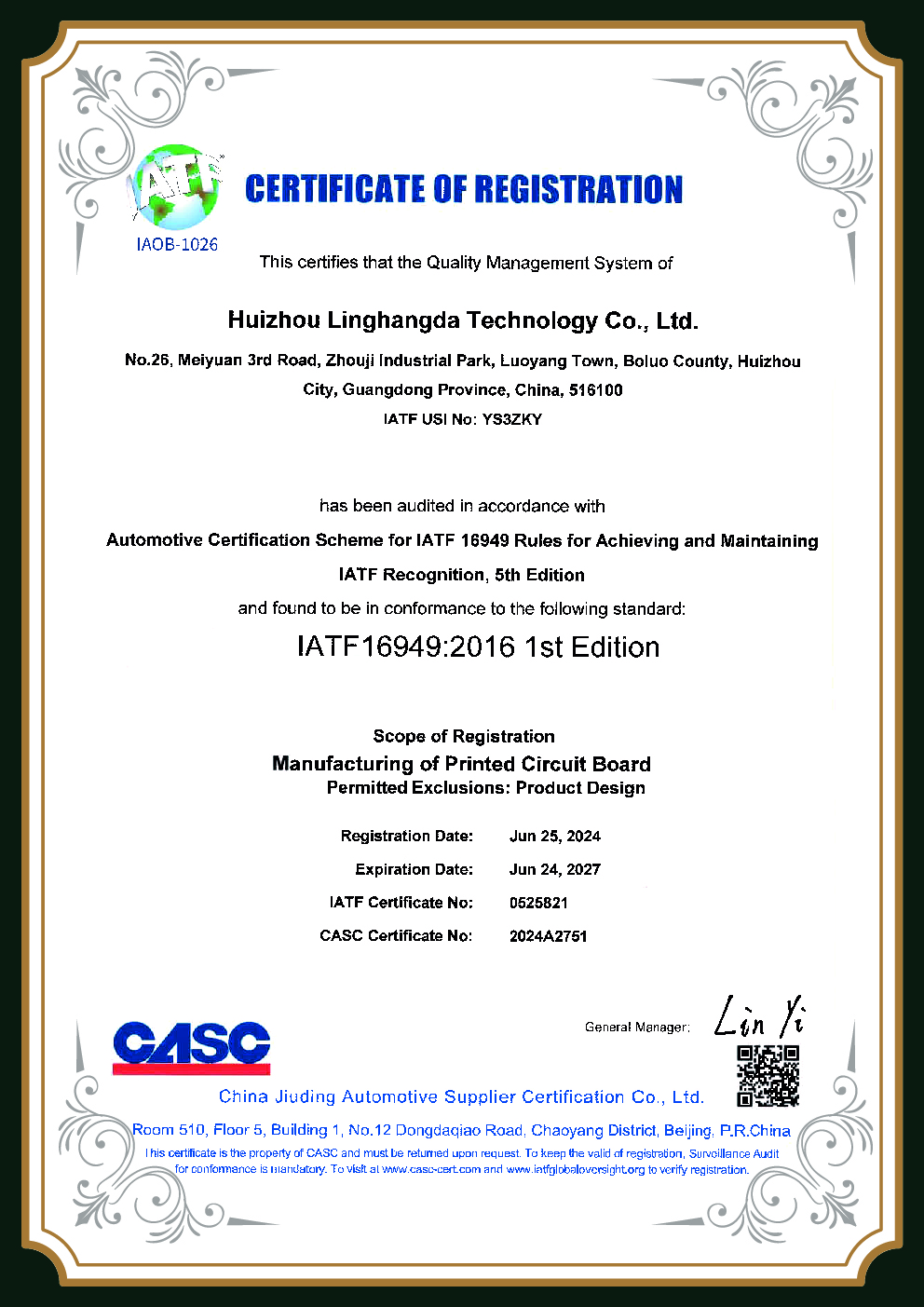
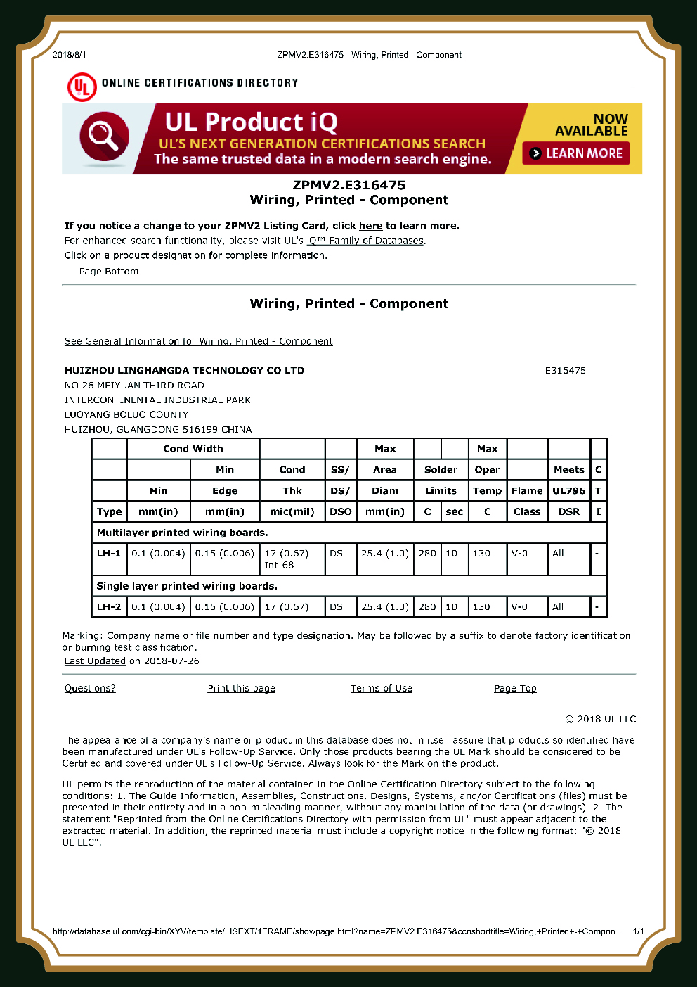
Trust on a high-layer board is earned through verifiable evidence, microsection reports, TDR data, coupon results, not geography. A recurring buyer fear is the outsourcing trap: a supplier that quietly subcontracts the complex high-layer work and isn’t up front about it. PCBark fabricates the 32–42 layer range on its own line in Huizhou, same factory, same line, so the equipment, the QA, and the certifications below describe the plant that actually builds your board.
Boards are built to IPC-A-600 and IPC-6012 Class 2 or Class 3 workmanship as the design specifies, these are the acceptance standards your board is fabricated against, applied per project as part of quality control across the whole of board manufacturing; the scope of these IPC Class 3 standards is published in detail. Our inspection stack carries the burden of proof on every high-layer lot:




High-layer boards warp when the copper distribution is unbalanced across the stack, so the build targets a symmetric copper layout to hold bow and twist within the documented ≤0.30%. The microsection then verifies, lot by lot, that registration and barrel plating actually landed where the stackup said they would. IPC-6012 Class 3 expects barrel fill ≥75% and limits plating voids to ≤5% of hole length for a single void, thresholds a cross-section coupon confirms directly rather than by claim.
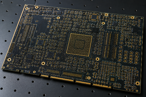
Rather than publish a price that can’t be accurate without your stackup, here’s the Pricing Factors Framework: the cost drivers that move a 32–42 layer quote, and how each one pushes it. Send the design, get a real number.
Each added pair raises material, lamination, and yield risk; cost rises non-linearly past ~30 layers
Megtron/Rogers stacks cost multiples of an FR-4 baseline; hybrid stacks moderate this
4–6 cycles vs one press — each cycle adds process time and cost
Adds a depth-controlled drilling step; needed above ~25 Gbps
Thick board + small holes stresses plating; higher ratio raises cost and yield risk
Each via type adds drill/plate/fill cycles between laminations
TDR coupons, microsection, and reliability testing add inspection cost — and prevent respins
Evaluate stackup material combinations and balance core thicknesses for ultra-high-density designs.
Calculate maximum drill depth to hole diameter ratios to ensure reliable copper plating in thick backplanes.
A rigorous pre-production audit framework to validate fabrication tolerances and yield reliability.
No, most fabs top out well below this tier. Verify the drilling and imaging equipment, and ask for a microsection coupon report before trusting any “up to 40+ layers” banner.
Look for ISO 9001 quality management, ISO 14001 environmental management, and IATF 16949 for automotive-grade process discipline, plus UL, RoHS, CE, and REACH compliance. Equally important, the boards should be built to IPC-A-600 and IPC-6012 Class 2 or Class 3 workmanship, with the acceptance class stated in writing. A certificate proves a system exists; it does not prove your specific high-layer lot met the class. Coupon evidence, a microsection cross-section, a TDR result, a registration coupon, matters more than the certificate count. Ask for both.
Pricing depends on layer count, low-loss material, number of lamination cycles, blind/buried vias, back-drill, aspect ratio, and testing depth. Industry sources place a 32-layer board near 12–18× a 2-layer baseline as a rough guide. An accurate figure comes only from your stackup, request a quote with Gerbers and an impedance spec.
Lead time scales with lamination cycles and via complexity, a 4-to-6-cycle build takes longer than a single-press board. A front-end DFM review prevents the respins that wreck schedules. Send your design for a stackup-specific timeline.
Inner layers are imaged with laser direct imaging, then bonded in 4–6 sequential lamination cycles. Blind and buried vias are drilled, plated, and copper-filled between cycles; high-aspect-ratio through-holes are drilled on CNC rigs and plated to ≥35µm. Back-drill removes stubs, and microsection plus TDR confirm registration and impedance.
Controlled impedance held to ±5%, tightly coupled differential pairs with adjacent ground planes, back-drilled via stubs, and low-loss dielectric manage signal integrity and crosstalk. Reliability comes from ≥35µm hole copper, ≤0.30% bow and twist, symmetric stack-ups, and lot-by-lot microsection plus TDR coupon verification, all of which protect pcb performance once the board reaches aerospace systems and other high-reliability hardware.
OKI Circuit Technology announced a 124-layer board in 2025, surpassing the long-standing 108-layer industry ceiling while holding a standard 7.6mm thickness, built for AI semiconductor wafer-test equipment. Earlier, Denso reported a 129-layer theoretical record in 2012. Those figures belong to research and test fixtures, not to anything you would ship inside a product. Commercial ultra-high-layer fabrication, boards that go into real HPC, telecom, and aerospace hardware at production yield, lives in the 32-to-42-layer tier, exactly where PCBark’s documented capability sits.
High-Tg FR-4, halogen-free systems, and low-loss laminates, Rogers, Isola, Panasonic Megtron, often in hybrid stacks that place low-loss dielectric only on the high-speed signal layers to manage cost.
PCBark’s core capability is in-house high-layer fabrication, with PCBA equipment available for assembly support including BGA placement, reflow, and X-Ray inspection of BGA joints. For a high-value high-layer board, discuss assembly scope during the RFQ so DFM and test coverage are planned together with fabrication.