Get in touch with PCBark Company

Multilayer PCB
Multilayer PCB Manufacturer (4–42 Layers) — Stackup, Fabrication & Turnkey Assembly
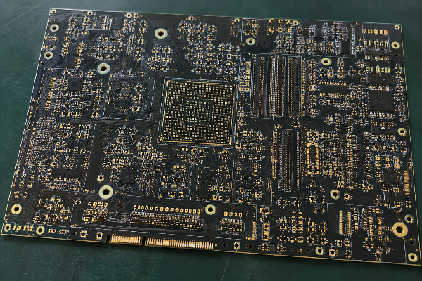
A multilayer PCB succeeds or fails in the stackup, not the sales banner. PCBark fabricates multilayer printed circuit boards from 4 to 42 layers on an in-house line, and publishes the full Standard-to-Maximum process capability so a buyer can size a board against real tolerances instead of a vague “high quality” claim.
This multilayer pcb hub exists to answer one question honestly: which layer count, material, and tolerance class does your board actually need, and can the fab prove it can hold them? Below are the capability numbers, a layer-count selection framework, a vendor-neutral comparison built on cited data, and a buyer-side verification method. Roughly half of the signal-integrity, power-integrity, and EMI problems engineers chase are preventable at the stackup stage, which is exactly where layer-count and reference-plane decisions get made.
4–42
Layer-count range (single line, 5 sub-tiers)
0.050mm
Min trace/space (Maximum tier)
±5%
Controlled-impedance tolerance
±35µm
Layer-to-layer registration
≥35µm
Plated hole copper (Class 3 +)
6
Certifications (ISO 9001 / IATF 16949 / UL …)
Turnkey
Fab + SMT/DIP/BGA + DFM + test
600×1200mm
Max board size
What a Multilayer PCB Is, and Why More Layers Isn’t the Goal
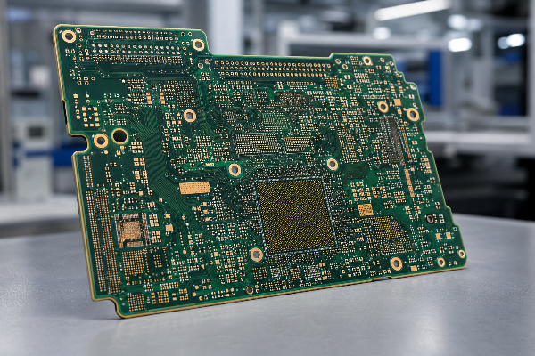
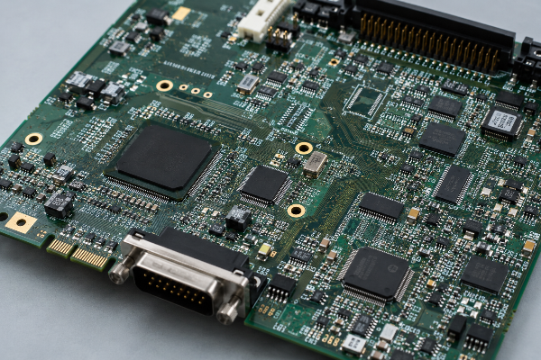
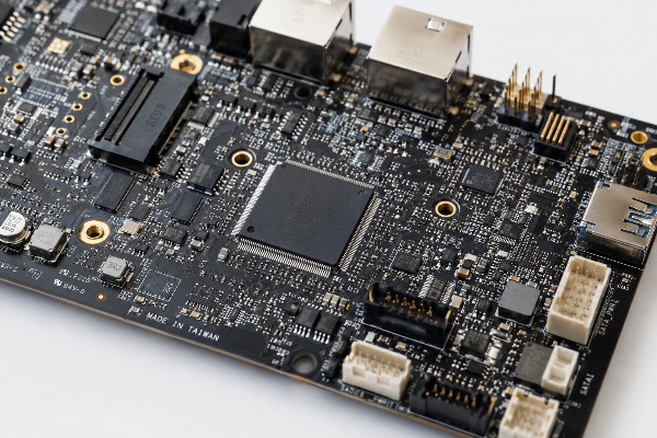
A multilayer PCB is a printed circuit board built from three or more conductive copper layers bonded into one structure, where the number of layers of conductive copper is separated by insulating material, prepreg and core dielectric, and joined into one electrical connection network by plated through-holes and blind or buried vias. The inner layers carry signal routing and dedicated ground and power planes that a single- or double-sided board can’t provide.
Among the common types of PCBs, a single-layer pcb carries copper on one layer, a double-sided board adds copper top and bottom, and multilayer boards (also written multi-layer pcbs) stack internal layers of conductive copper for the routing density modern electronics demand. Multilayer pcbs are used wherever copper traces, passive components, and active electronic devices outgrow the two outer layers, most complex circuits in computing, telecom, automotive, and medical hardware are multilayer for exactly that reason, bonding the layers together into a single rigid board.
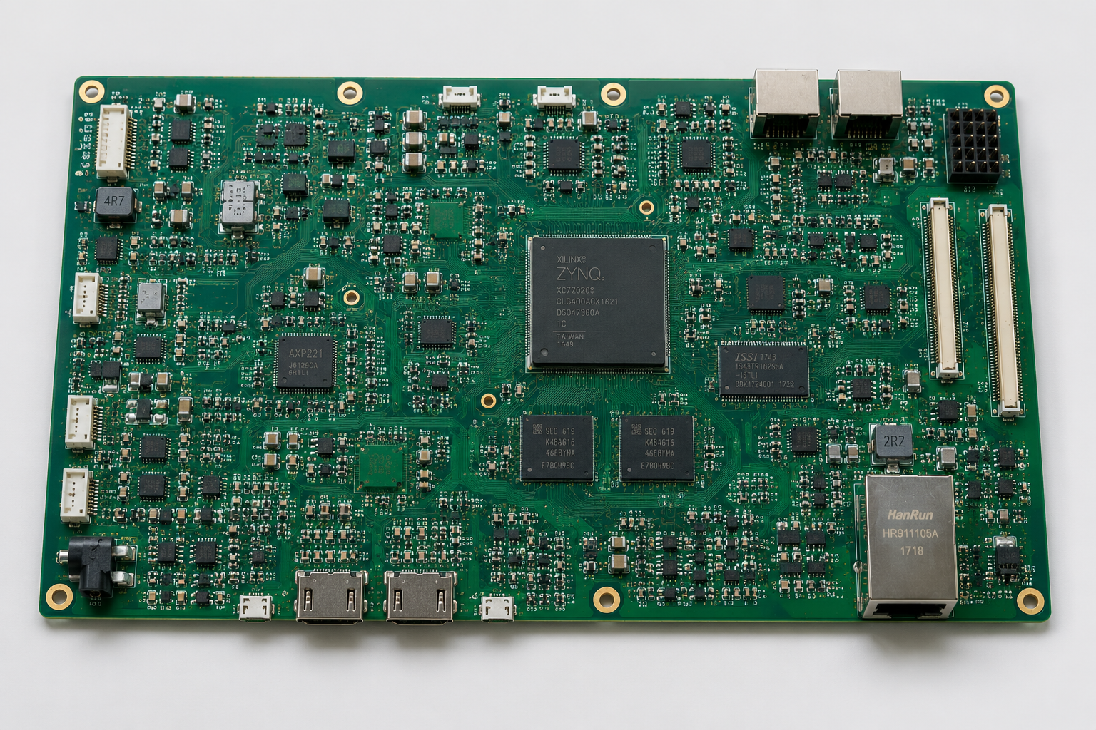
Most buyers arrive asking for more layers. The more useful question is whether the design driver justifies them, because adding copper layers isn’t a free upgrade. Components still mount only on the outer two layers, so a higher layer count doesn’t shrink the board the way buyers expect, one engineer’s rule of thumb puts a 4-layer board at up to 20×16 in of usable area against roughly 16 layers at roughly 12×10 in once you reach 16 layers. And reliability doesn’t improve with layer count either: every added interlayer interconnection is one more thing that can open in the field, so the probability of a latent failure rises, not falls, as the stack grows. Practitioner discussion is blunt that a high-layer board is often a last resort, not a default.
The honest frame is this: layer count should follow the routing density, the controlled-impedance pair count, the power-domain count, and the reference-plane requirement, never the other way around. A 4-layer multilayer pcb with a thick core and a Sig/Gnd/Pwr/Sig stack is a common default, yet it couples power and ground poorly across that thick center; sometimes the right answer is a better-balanced 6-layer stack, not a thicker 4-layer one. Where the driver is real, multilayer printed circuit boards become the difference between a manufacturable board and a respin. PCBark’s role on a quote is to confirm the layer count is right-sized first, then build it to spec.
The 4-to-42 Layer Selection Decision Tree
Pick the layer count from the design driver, not the spec-sheet ego. This decision tree maps the signal, power, and density requirement to a recommended layer tier, then routes you to the matching product page. The standard FR-4 process tops out near 8–10 layers before board thickness has to grow, and the BGA pitch is usually what forces the jump: once you cross a 0.8 mm pitch, via-in-pad and HDI construction enter the picture.
Layer-count decision tree — design driver → recommended tier
If your design has…
Recommended layer count
Why
Simple control, consumer/IoT, no high-speed
2–4 layers
One plane pair gives a clean ground reference at lowest cost
One or two high-speed buses (DDR, Ethernet), moderate density
6 layers
Dedicated planes isolate signals; DDR5 routing realistically needs 6+
Several controlled-impedance buses, dense BGA ≥ 0.8 mm pitch
8–12 layers
Multiple routing layers between plane pairs keep return paths short
High pin-count BGAs, many power rails, fine pitch < 0.8 mm
16–24 layers
Dense fan-out + plane shielding; HDI/buried vias recover routing space
HPC/AI backplanes, 400G–800G telecom, aerospace backbones
32–42 layers
Sequential lamination + low-loss laminate; the high end of the ladder
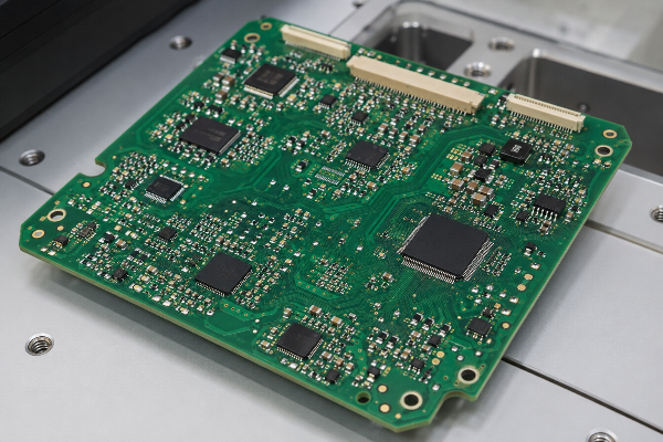
4-Layer PCB
- Sig / GND / PWR / Sig standard stack
- Quick-turn 24h available
- FR-4 / High-Tg FR-4
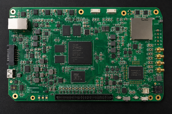
6-Layer PCB
- Signal-integrity-optimized stackups
- For DDR / Ethernet / RF buses
- Controlled impedance ±8%
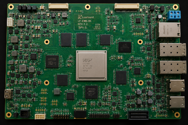
8-12 Layer PCB
- Industrial, networking, high-speed digital
- Multiple isolated buses
- Stackup + SI verification support
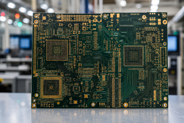
16-24 Layer PCB
- Servers, telecom switches, advanced industrial
- Sequential lamination + low-loss laminate
- Blind / buried vias
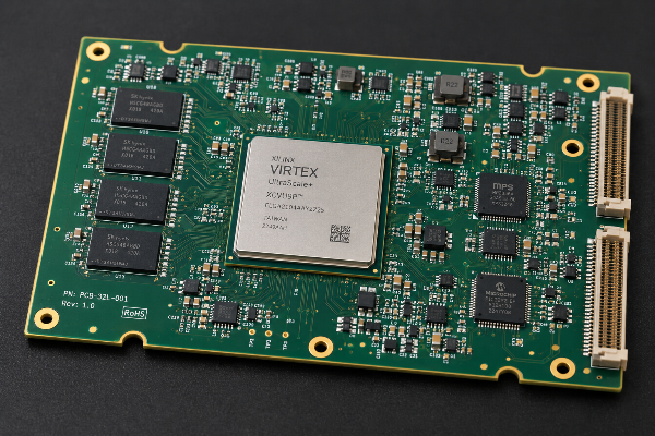
32-42 Layer PCB
- HPC / AI server & telecom backplanes
- 4–6 lamination cycles, ±5% impedance
- Industry-top documented tier
Not sure which layer count your board needs?
PCBark vs Typical Multilayer Suppliers, Capability & Cost of Ownership
Buyers compare multilayer pcb manufacturers on a banner, then get surprised by what the banner left out. The most common gap across competitor product pages is that almost none publish a data-driven comparison against an external reference, so here’s a vendor-neutral table built on cited engineering data, with PCBark’s documented numbers placed against the industry baselines a buyer can verify independently.
Multilayer capability vs cited industry baselines
| Capability Axis | Industry Baseline (Cited) | PCBark Documented |
|---|---|---|
| Min trace/space (high-end) | 0.1 mm common production floor | 0.050 mm (Maximum tier) |
| Controlled-impedance tolerance | ±10% standard, ±5% premium | ±5% (Maximum) |
| Plated hole copper | IPC-6012 Class 3 min ≥25 µm (1.0 mil) | ≥35 µm |
| Layer-to-layer registration | ≤50 µm typical accepted | ±35 µm |
| Quality system | ISO 9001 = entry baseline | ISO 9001 + ISO 14001 + IATF 16949 |
| Scope | Many fabs are bare-board only | Turnkey: fab + SMT/DIP/BGA + test |
| Capability transparency | Single column or undisclosed | Published 3-tier envelope |
Total cost, not unit price
The honest version is that the cheapest quote isn’t the cheapest board, and the lowest unit price often compromises total cost. Multilayer cost rises non-linearly with layer count, and one PCB designer’s measured data puts a 14-layer board near 5–6× the per-area cost of a 4-layer at volume, and around 12× at low quantity. The hidden costs that actually erode a budget are a respin from a missed DFM issue, a mid-contract price change, or a board that bricks because an inner layer was wrong. A turnkey single source removes the fab-to-assembler hand-off where many of those defects hide: one BOM, one DFM review, one party accountable from Gerber to tested board. For a fine-pitch design, a denser HDI stackup that drops two layers can even land cheaper at the whole-board level, because the saved laminate and lamination cycles offset the higher unit price.
Want this comparison run against your specific stackup and volume?
Request a custom capability & cost comparison →
Application-to-Stackup Compatibility Heatmap,
Best Layer Count by Industry
Layer count is an application decision before it’s a fabrication decision. This heatmap maps the industries PCBark builds for to the layer range, material class, and finish those boards call for, so you can sanity-check your own design against how the field maps layer count to application for that use case. It also answers the “best for X” question buyers ask AI assistants: which multilayer construction fits which job.
[APP-01]
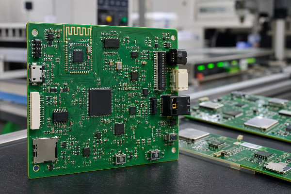
Consumer electronics & IoT
LAYERS
2–6
MATERIAL
FR-4 / High-Tg
FINISH / NOTE
HASL-LF / ENIG — cost-driven volume
[APP-02]
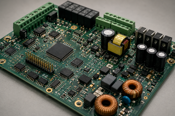
Industrial control (PLC, motor drives)
LAYERS
4–16
MATERIAL
High-Tg FR-4
FINISH / NOTE
ENIG — IATF 16949, IPC Class 2/3
[APP-03]
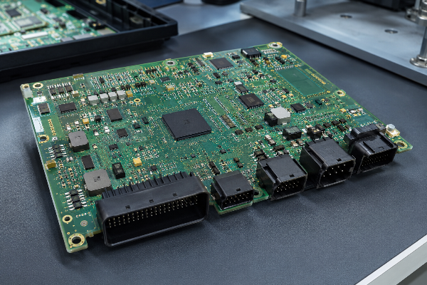
Automotive electronics
LAYERS
4–16
MATERIAL
High-Tg, halogen-free
FINISH / NOTE
ENIG / ENEPIG — IATF 16949 discipline
[APP-04]
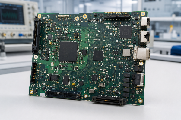
Medical & test instrumentation
LAYERS
6–24
MATERIAL
High-speed laminate
FINISH / NOTE
ENIG / Imm Ag — IPC Class 3
[APP-05]
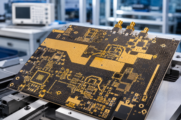
RF / high-frequency (5G, radar)
LAYERS
6–16
MATERIAL
Rogers, PTFE hybrid
FINISH / NOTE
ENEPIG — impedance ±5%
[APP-06]
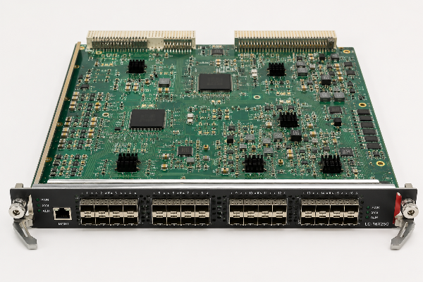
Networking / telecom line cards
LAYERS
8–24
MATERIAL
Low-loss / Megtron
FINISH / NOTE
ENEPIG — many differential pairs
[APP-07]
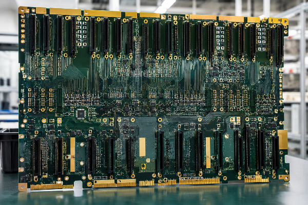
Servers, HPC & AI backplanes
LAYERS
24–42
MATERIAL
Megtron, Isola, hybrid
FINISH / NOTE
ENEPIG / hard gold — seq. lamination
[APP-08]
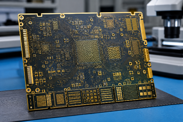
Aerospace & defense backbones
LAYERS
high-layer
MATERIAL
Exotic low-loss
FINISH / NOTE
Hard gold — Class 3, full coupon evidence
Quality & Reliability,
How Every Multilayer Board Is Tested
The multilayer failure buyers fear most is the one you can’t see: an inner layer that was wrong, a barrel that cracks under thermal cycling, an impedance that drifted out of spec. One buyer’s account of a bad lot is exactly this — “the vendor didn’t add inner layers, the boards bricked, and they refused to refund.” A certificate can’t catch that; coupon evidence and in-line inspection can. PCBark carries the burden of proof on every multilayer lot with a layered quality control and inspection stack, not a single final check.
01
PAIN
Inner-layer and hidden-via defects on multilayer boards pass a visual check and fail in the field.
02
CAUSE
Buried features and plated barrels can’t be confirmed from the outside; final-only QA misses them.
03
SOLUTION
Inner-layer AOI, X-Ray on buried vias, flying-probe E-test, and TDR impedance coupons per lot.
04
PROOF
Metallographic microsection reads registration and barrel copper against IPC-6012 acceptance.
INSPECTION STACK
- AOI automated optical inspection on inner and outer layers, before and after etch
- X-RAY confirms buried-via fill and internal alignment a surface check can’t see
- FLYING-PROBE & 100% E-TEST netlist verification on every board
- TDR IMPEDANCE controlled-impedance confirmation with Type-Z coupons, not just a spec on paper
- METALLOGRAPHIC MICROSECTION reads layer-to-layer registration, bond lines, and plated barrel copper
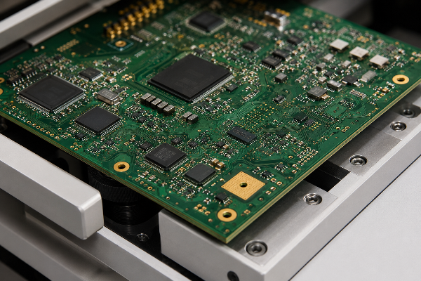
Certifications & Compliance, Evidence Over Geography
For a US or European buyer, the real question behind “made in China” isn’t the map pin, experienced buyers will tell you the finest board shops in the world include Chinese fabs, and that quality is a non-issue with the right one. The real risks are unspecified substitutions and an unverifiable acceptance class. PCBark answers both with a named certification stack and written workmanship standards, applied through its own in-house PCB manufacturing rather than a quiet subcontract.
-
ISO 9001
Quality management system
-
ISO 14001
Environmental management
-
IATF 16949
Automotive quality system
-
UL
Listed laminate & process
-
RoHS
Restricted substances
-
CE / REACH
EU conformity & substances







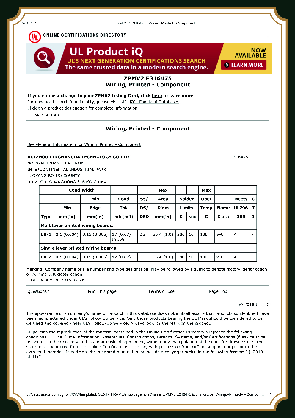
Verification Protocol
IATF 16949 is the differentiator worth noting: it’s the automotive-grade process-discipline standard, and many multilayer competitors that serve automotive don’t actually hold it. Behind these systems, the boards are built to the recognized acceptance documentsISO 9001 for the quality system and IPC-A-600 / IPC-6012 for the board itself. A certificate proves a system exists; it doesn’t prove your lot met its class. That’s why PCBark pairs the certificate set with lot-level coupon evidence, the combination is what turns a compliance list into a verifiable commitment.
Procurement, Lead Time, Pricing Drivers & Turnkey Multilayer PCB Manufacturing
Lead time is the number-one reason engineers switch multilayer suppliers. As one put it, “I switched from one supplier to another due to production and shipping speed” — five-to-six weeks down to two, and never looked back. That’s the honest trade-off buyers weigh against headline price. A late board misses a market window; a respin from a skipped DFM review is worse. Rather than publish a price that can’t be accurate without your stackup, here’s the Pricing Factors Framework, the drivers that move a multilayer quote and how each one pushes it, plus exactly what to send for an accurate number.
What moves a multilayer PCB quote
Pricing Factors Framework
Layer count
Primary driver; rises non-linearly — each added pair adds material, lamination, and yield risk
Base material
Rogers / Megtron low-loss stacks cost multiples of an FR-4 baseline; hybrids moderate it
Via strategy
Blind and buried vias add drill/plate/fill cycles between laminations
Tolerance / impedance control
Tighter trace and ±5% impedance add process control cost
Surface finish
ENIG / ENEPIG / hard gold step up from HASL per unit area
Volume & board size
Panel utilization and quantity set the per-board floor
Testing depth
TDR coupons, microsection, and reliability testing add cost — and prevent respins
Process: Turnkey Path
The turnkey path is where total cost actually drops. PCBark runs the full chain in-house, front-end DFM, transparent component sourcing through authorized distributors, fabrication, SMT / DIP / BGA multilayer PCB assembly, and functional test, so a multilayer board moves from BOM to a tested assembly under one roof, whether you need a quick-turn prototype or a high-volume run. These end-to-end PCB manufacturing services remove the fab-to-assembler hand-off where shortages, substitutions, and finger-pointing tend to live, and it’s why the spec-lock matters: the build sheet records the exact material and impedance target, and the order is fabricated to it.
What to send for an RFQ
- Gerber / ODB++ fabrication files
- Layer stackup layer count, dielectric thicknesses, copper weights
- Material preference (FR-4 / High-Tg / Megtron / Rogers / hybrid) with Tg called out
- Impedance spec single-ended and differential targets with tolerance
- Requirements Any blind, buried, or back-drill requirements, plus the IPC class
Multilayer PCB Engineering Calculators
-
Layer Count Recommender
Determine the optimal number of layers based on signal density, routing requirements, and component placement.
Access Tool -
Multilayer Cost Factor Estimator
Evaluate the financial impact of material choices, layer counts, and advanced manufacturing processes on your budget.
Access Tool -
Controlled Impedance Estimator
Calculate trace widths and spacing to achieve precise impedance control for high-speed signal integrity.
Access Tool
Sourcing a multilayer PCB? Send the stackup.
Get a front-end DFM review and a quote built on your real design, layer count right-sized, material and impedance locked, and capability verified against a documented 4-to-42-layer process envelope.
Request a QuoteA multilayer PCB is a printed circuit board with three or more conductive copper layers bonded into a single board with insulating prepreg and core between them, interconnected by plated through-holes and blind or buried vias. The inner layers add signal-routing layers and dedicated ground and power planes that single- and double-sided boards can’t offer, which is what enables higher density and controlled impedance.
A 4-layer board gives one inner plane pair (signal / ground / power / signal). A 6-layer board adds a second plane pair, so high-speed signals can be routed as stripline between solid reference planes with cleaner return paths and better impedance control. If you’re routing DDR, multiple high-speed buses, or need stronger EMI isolation, 6 layers is usually the right step up; for simpler designs, 4 layers is more cost-effective.
Not automatically. Components still mount on the outer two layers, so more layers don’t shrink the footprint, and field-failure probability actually rises with interlayer interconnections. More layers help only when routing density, controlled-impedance pair count, or power-domain complexity genuinely exceed what fewer layers can route with clean return paths. Right-sizing the layer count is part of a good DFM review.
A blind via connects an outer layer to one or more inner layers without passing through the whole board; a buried via connects only inner layers and is invisible from the surface. Both are formed with sequential lamination and free up routing space that full through-holes would block, essential for high-density and high-layer multilayer boards. They add cost because each via type adds drill, plate, and fill cycles between laminations.
Look for ISO 9001 (quality management), ISO 14001 (environmental), and IATF 16949 for automotive-grade process discipline, plus UL, RoHS, CE, and REACH. Just as important, boards should be built to IPC-A-600 and IPC-6012 Class 2 or Class 3, with the class stated in writing. A certificate proves a system exists; a microsection or TDR coupon proves your specific lot met its class, ask for both.
The multilayer PCB manufacturing process combines several manufacturing techniques in sequence. Inner conductive layers are imaged and etched, then bonded with prepreg in a heat-and-pressure lamination cycle (several sequential cycles for high-layer or HDI builds). Holes are drilled, desmeared, and plated with copper; outer layers are patterned and etched; solder mask and surface finish are applied; then the board is electrically tested. This pcb manufacturing process forms blind and buried vias, drilled, plated, and filled, between lamination cycles.
Cost is driven mainly by layer count, which rises non-linearly, a designer’s measured data points to roughly 5–6× the per-area cost from 4 to 14 layers at volume, and more at low quantity. Material (FR-4 vs Rogers/Megtron), via strategy, impedance tolerance, finish, and volume move it further. An accurate figure comes only from your stackup, send Gerbers and an impedance spec for a quote.
OKI Circuit Technology announced a 124-layer PCB in 2025, roughly a 15% increase over the long-standing 108-layer ceiling, at 7.6 mm thickness for AI semiconductor wafer-test equipment. Those figures belong to test fixtures, not products you ship. Commercial high-layer production, boards that go into real HPC, telecom, and aerospace hardware at yield, runs in the 32-to-42-layer range, which is the top tier of PCBark’s documented capability.
Yes. PCBark provides fabrication plus turnkey PCB assembly, SMT, DIP, and BGA placement with X-Ray inspection of BGA joints, component sourcing through authorized distributors, and functional test, so a board moves from BOM to tested assembly under one roof. Discuss assembly scope during the RFQ so DFM and test coverage are planned together with fabrication.

![High Frequency PCB Guide: RF & Microwave Design [2026]](https://pcbark.com/wp-content/uploads/2026/07/rf-microwave-pcb-guide-featured-1-150x150.png)