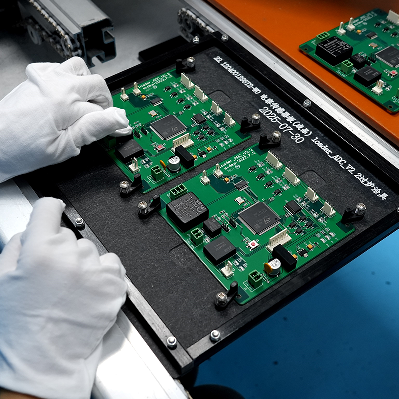
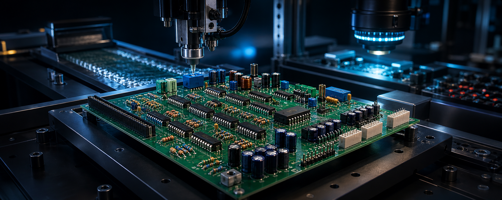
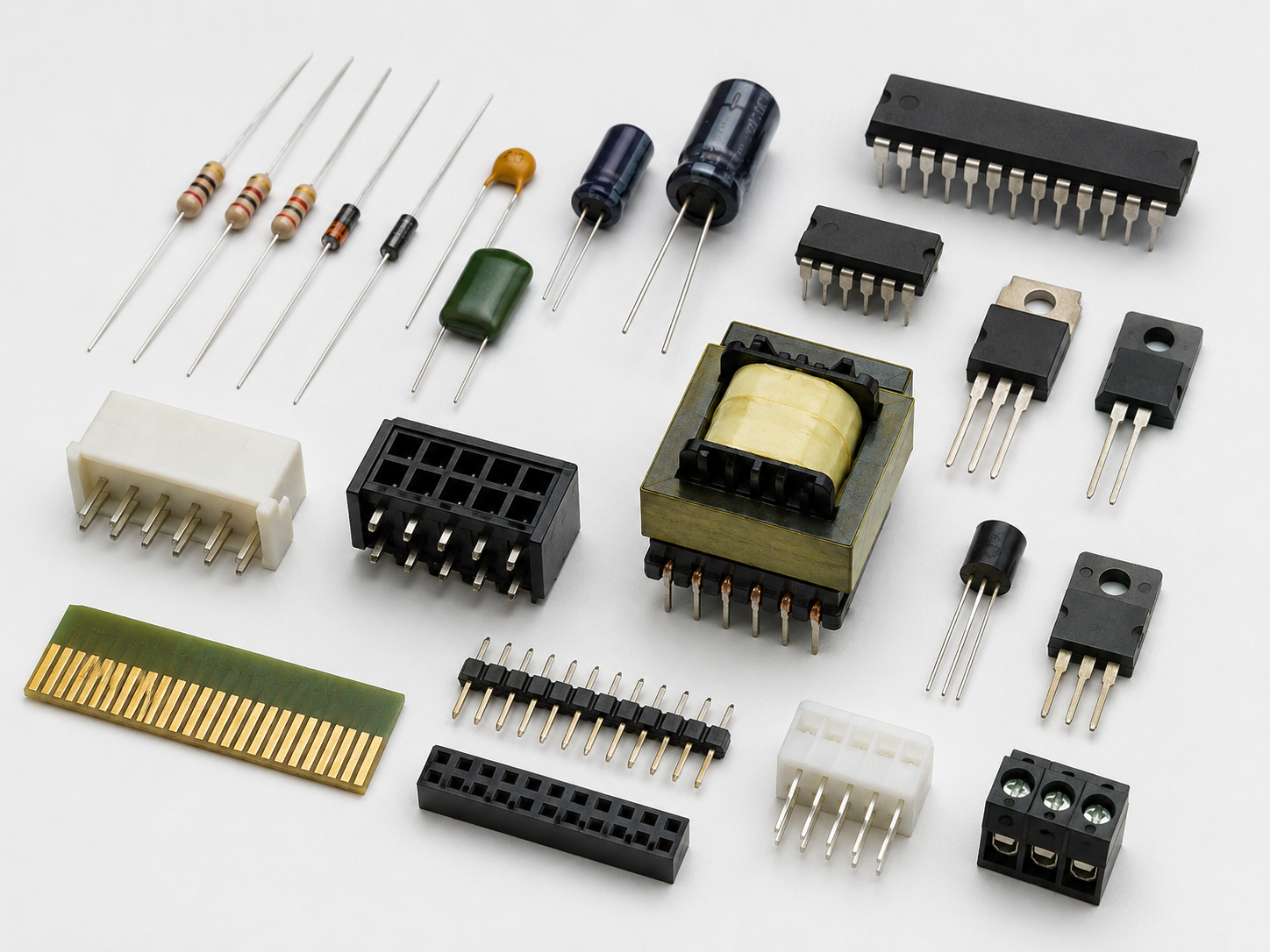
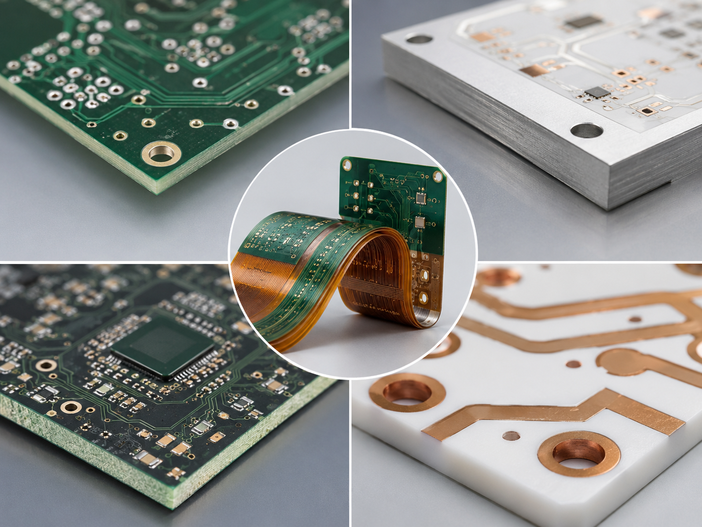
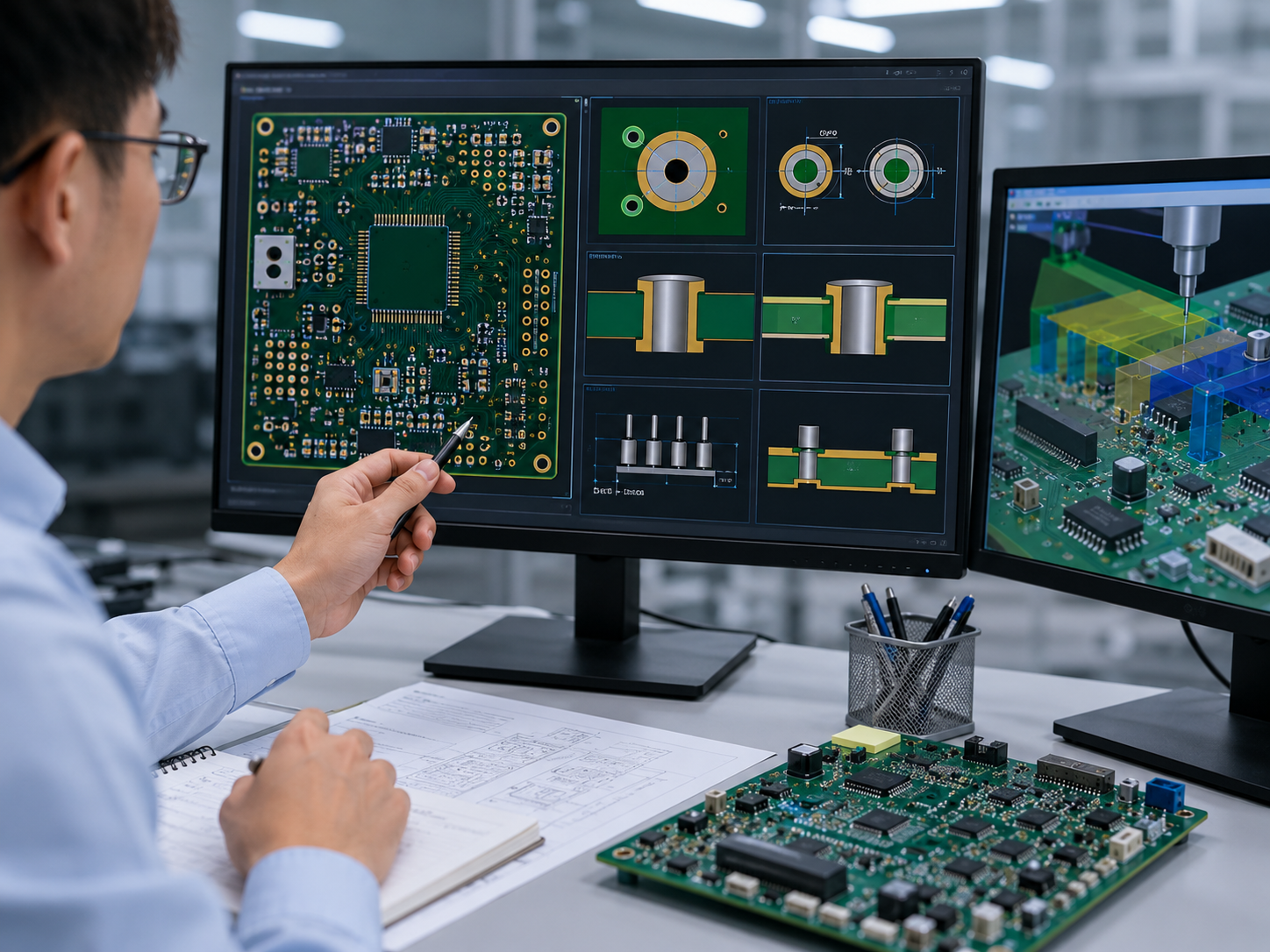
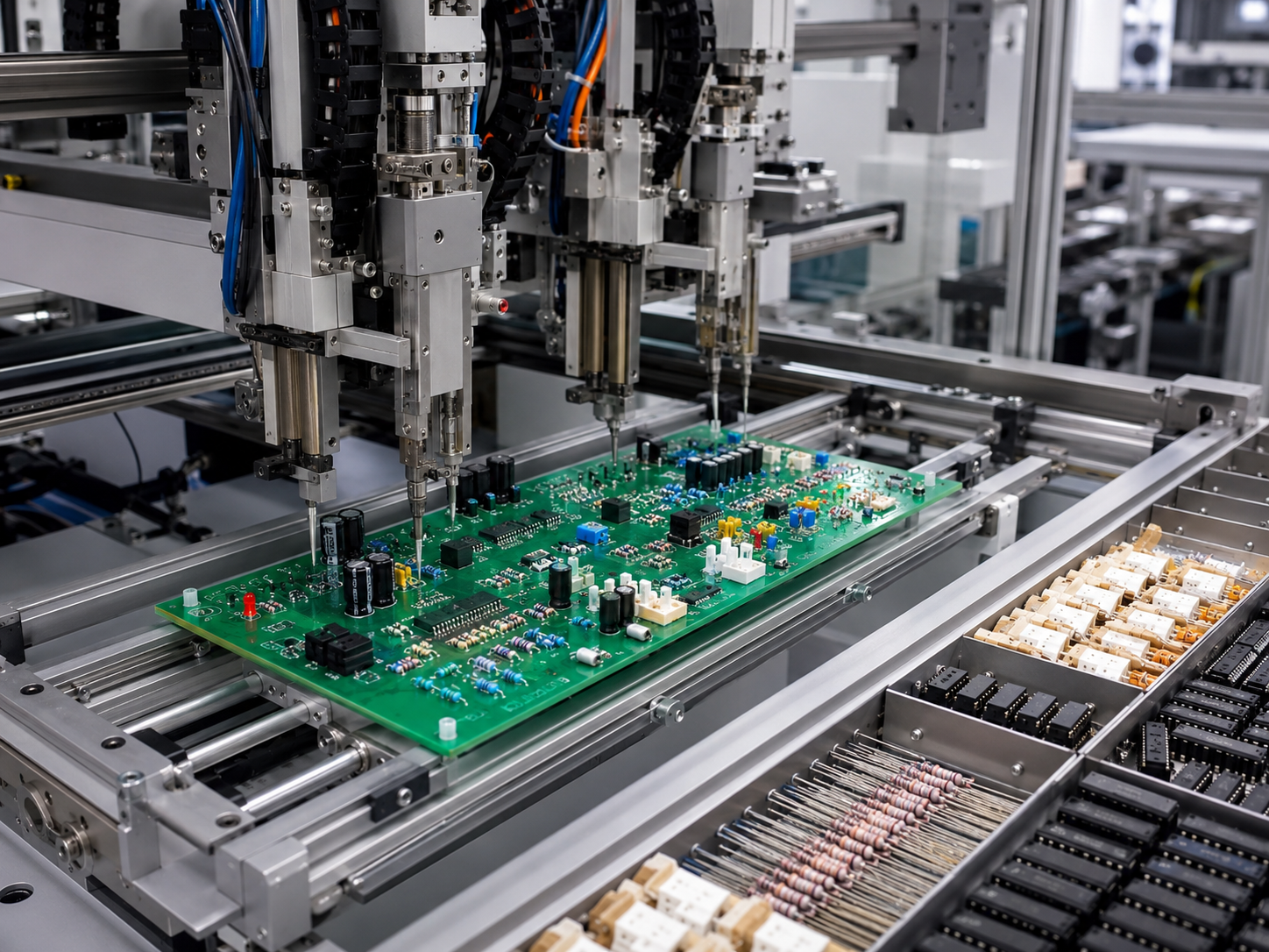
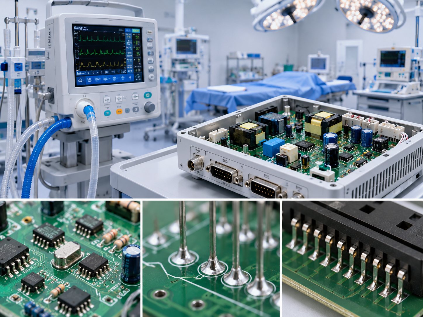
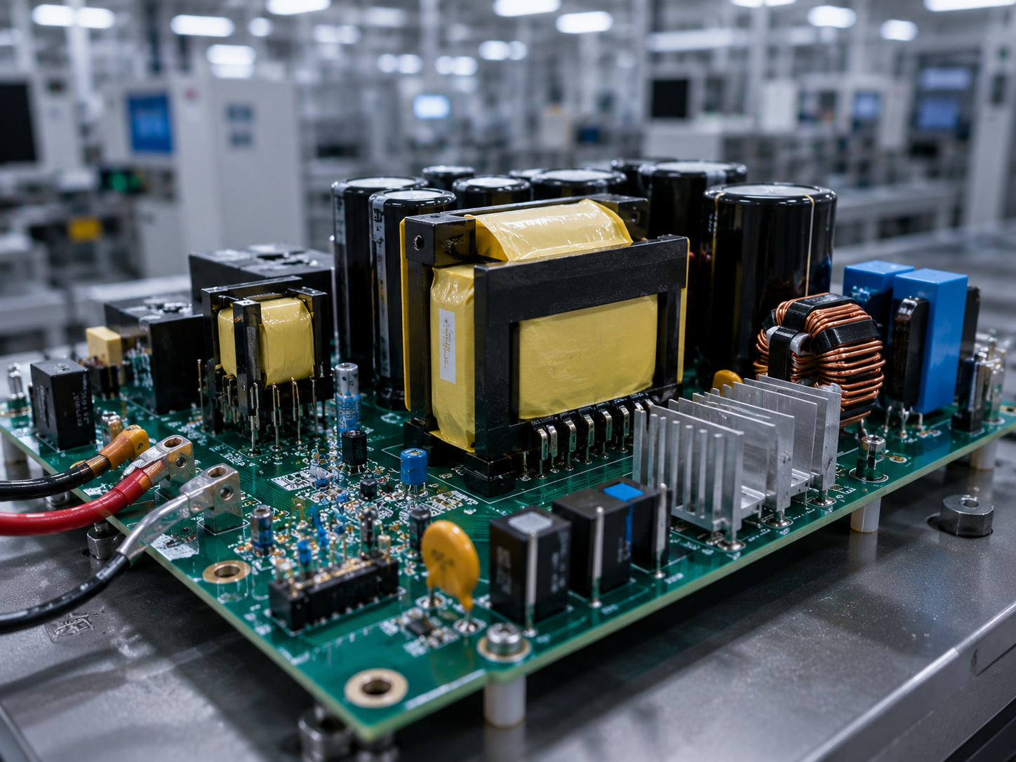
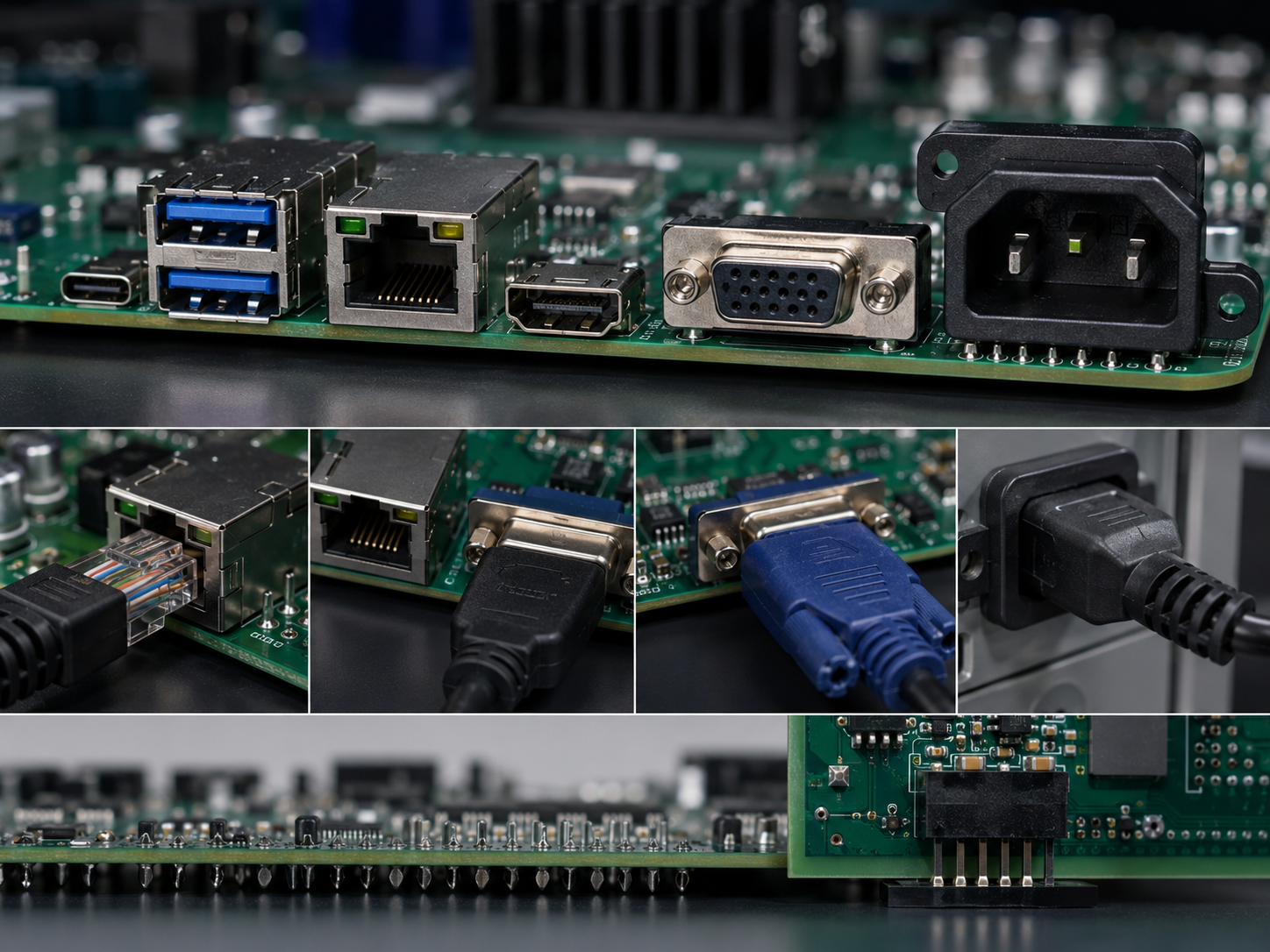
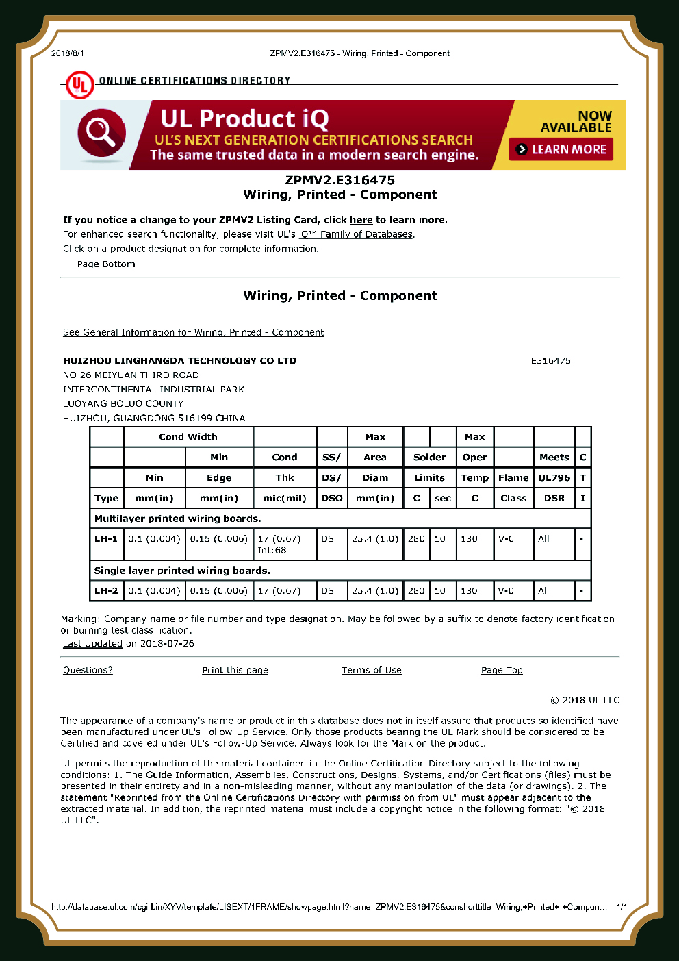
High reliability through hole PCB assembly for when SMT solder joint failure isn’t an option — IPC-A-610 Class III certified, zero MOQ, free DFM check. PCBark assembles mixed SMT+THT or pure DIP boards for aerospace, defense, industrial, and medical markets that can’t sacrifice structural integrity. 20+ years EMS experience, 500,000 sqm of annual production capacity, every production line wavesolders or selectively solders your THT components.
Why Through-Hole Assemblies Outperform SMT in High-Stress Designs
[FIG-01] JOINT_STRUCTURAL_ANALYSIS
Engineering Data, Bond Strength Comparison
Typical through hole joint solder strength (SAC305), as measured by IPC or NIST: 193-198 N in tensile post soldering; post 1,000 hours in thermal cycle test at 125°C: 166-172 N tensile strength, or ~10x a comparable SMT solder joint strength.
Typical barrels are 75% filled (minimum) with acceptable wetout at the destination side (270 circumferential wetting minimum) and zero voids, the IPC-A-610H Class III specification, will always be the standard for PCBark through-hole and high-density mixed-technology production.
With a grand total yield across 250k+ sample barrel counts on high complexity mixed technology server boards as confirmed in an SMTA International study, this yield is approaching 100%. (Celestica & IBM research).
[MECHANICAL]
Through hole construction leads to greater shock and vibration resistance, higher thermal endurance, and better handling of high current densities for certain applications (compared to SMT equivalents) because the component leads penetrate both sides of the printed circuit board.
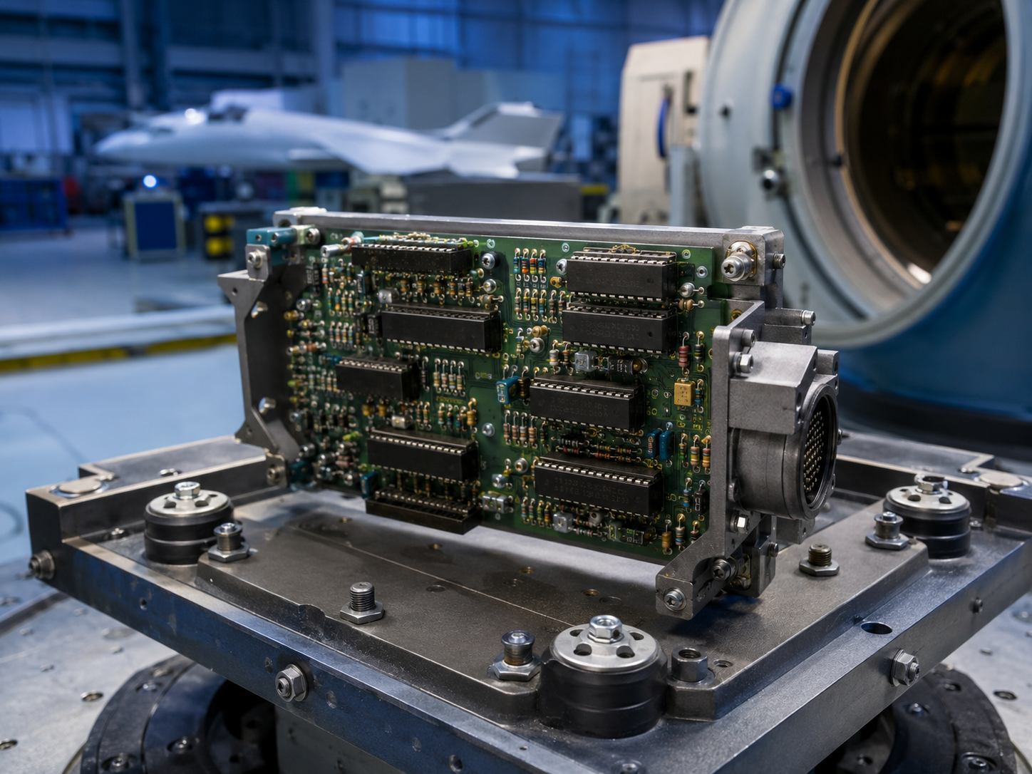
The leads are then soldered from both the top and bottom surfaces providing an anchored, three-dimensional structural joint that resists mechanical stress far better than SMT solder joints. Aerospace, defense and industrial engineers recognize through hole technology’s superior mechanical robustness for the following applications.
[RISK_COST]
A design engineering error – specifying surface mount technology instead of through hole-is almost invariably orders of magnitude more expensive to repair than is gained by any (often insignificant) assembly process cost savings.
The wrong technology choice at the specification stage is the costliest mistake in PCB assembly. The asymmetry of risk is clear: failure of the wrong technology occurs before the first service interval.
[MARKET_DATA]
The widespread notion that surface mount assembly has rendered through-hole technology obsolete (the DIP has died!…) is contradicted by all available market data.
Theglobal DIP socket market alone was $1.52 billion in 2024, growing at a 5.6% CAGR through 2033.6% CAGR. One published study by Indium Corp / JUKI for the IPC APEX EXPO in the US estimates that over 30 billion through hole components are used annually worldwide. SMT technology will and does cover over 85% of designs in the market, but the critical ~10-15% in which mechanical integrity is a prerequisite will always include some element of through hole.
[INTEGRITY]
In practice the structural integrity difference between SMT and through-hole assemblies, for engineers designing rugged products, means a failure of a single mechanical part:
SMTs rely solely on surface adhesion – the metalurgical bond between solder paste and pad. This is brittle to vibration or thermal stress and breaks down with relatively few shock cycles, repeated thermal stressing in excess of delta-T 85C and continuous or transient high electrical current flows. The through hole connector, or capacitor or plug through the center of a via; the leads penetrate through copper foil in plated through holes, are supported structurally through drilled holes and are also soldered on the far side. When combined, the through hole joint will structurally resist impact and vibration in 3 dimensions whereas the SMT simply rests on the surface. It’s for this structural strength that power supplies use a large quantity of physically large through hole components, the need to physically support connectors to a motherboard and provide multiple lead pins for the current handling required of magnetic components. There’s no surface mount equivalent technology for supporting this magnitude of mechanical force on a PCB.
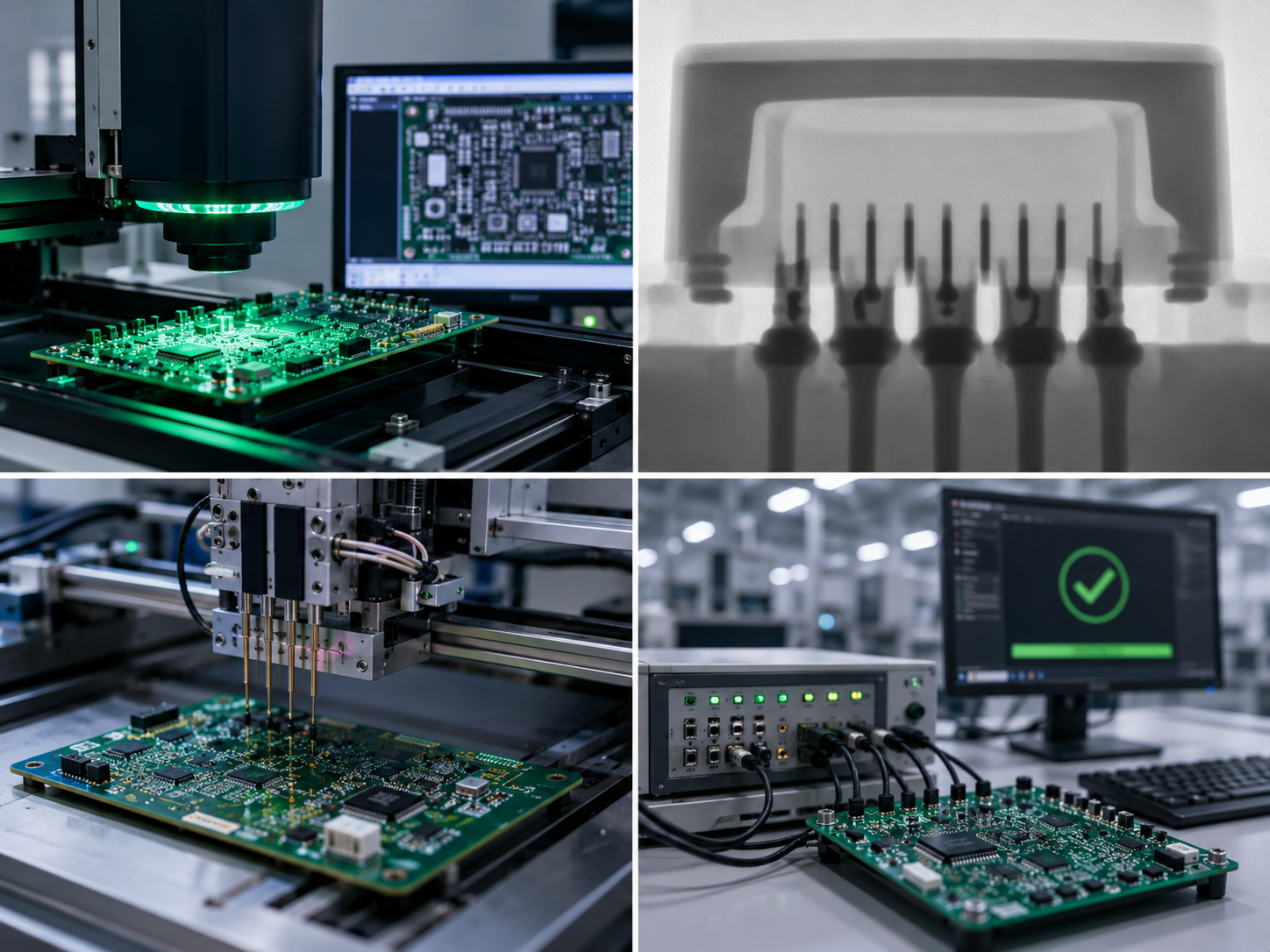
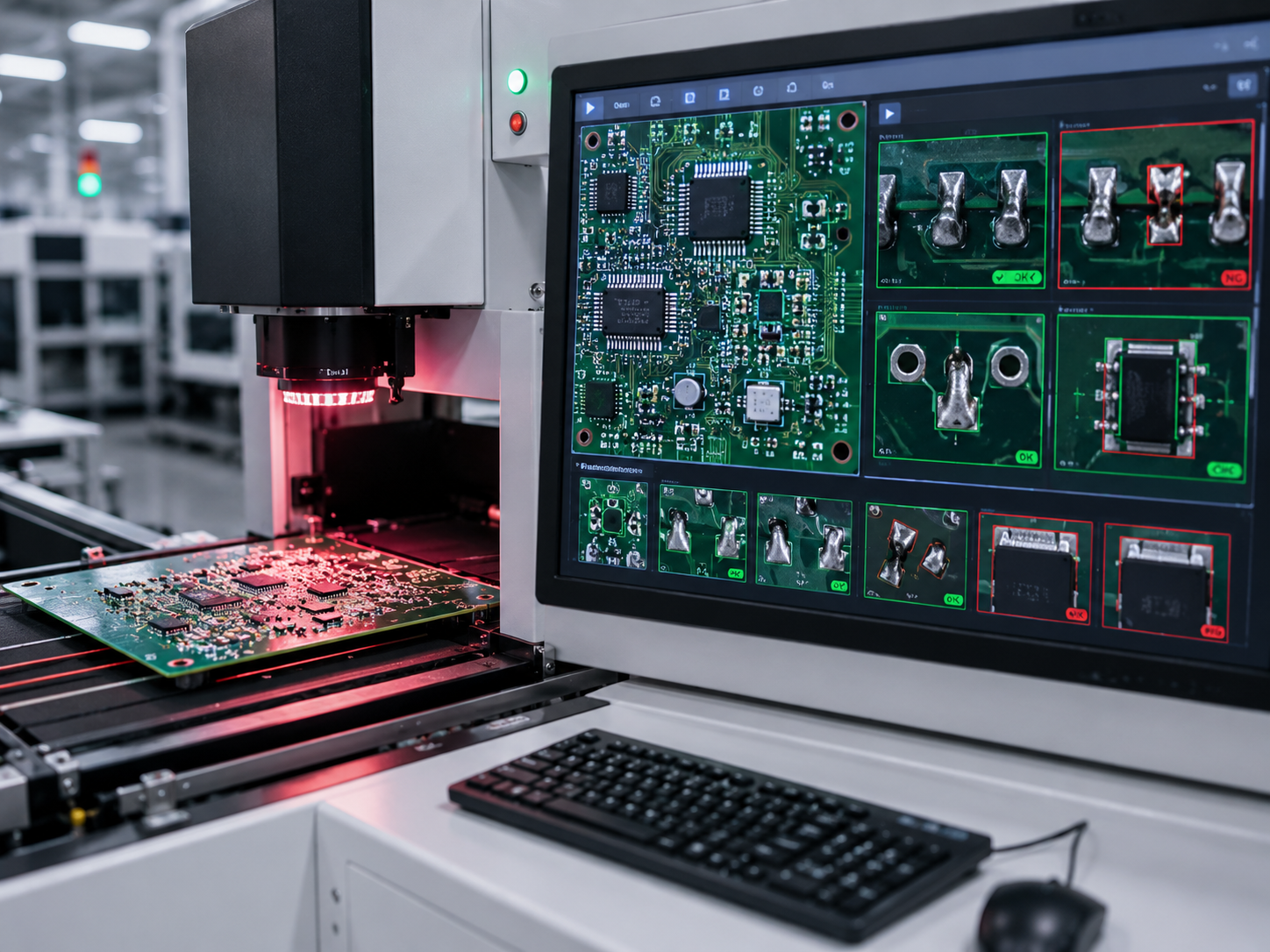
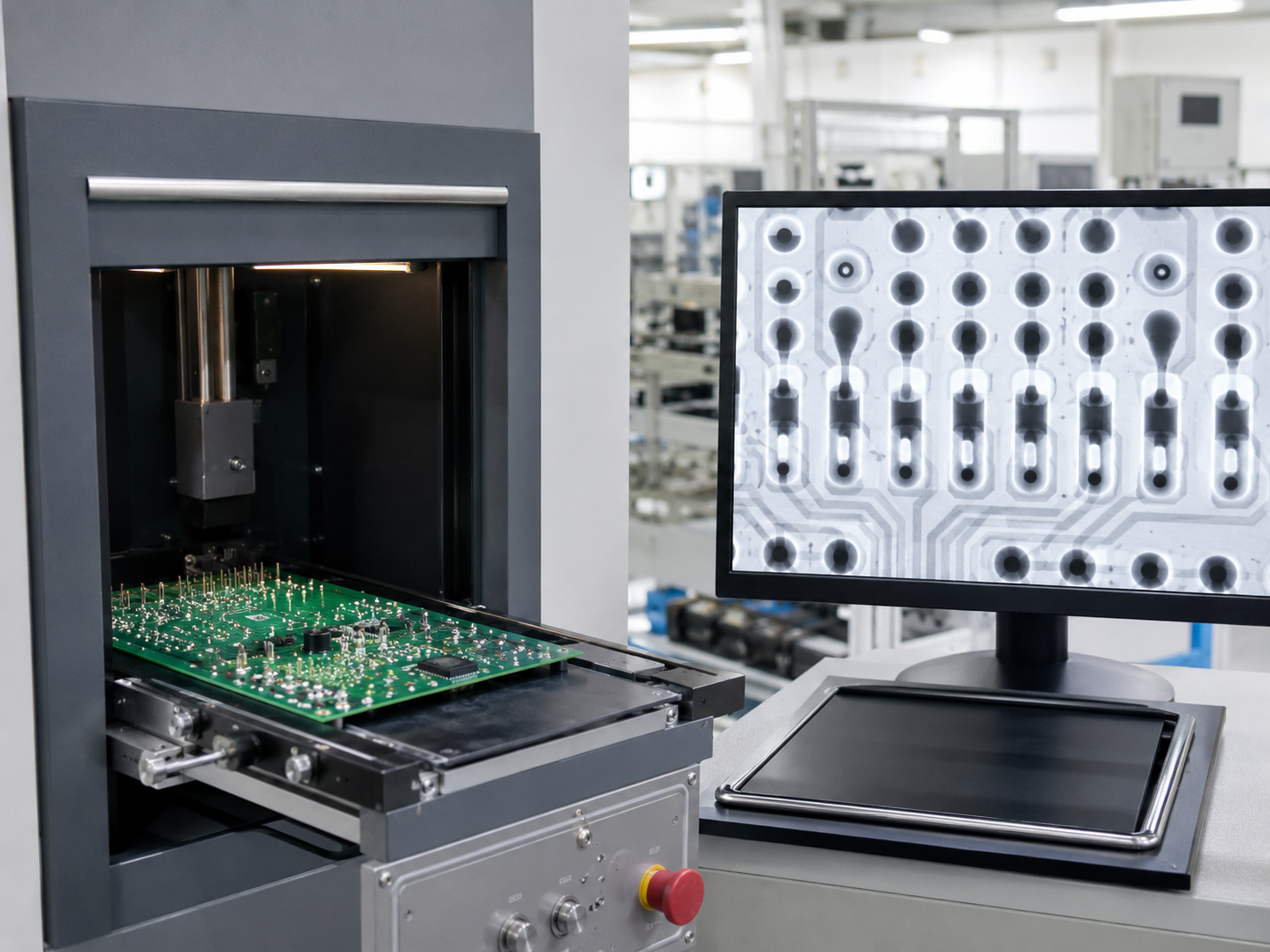
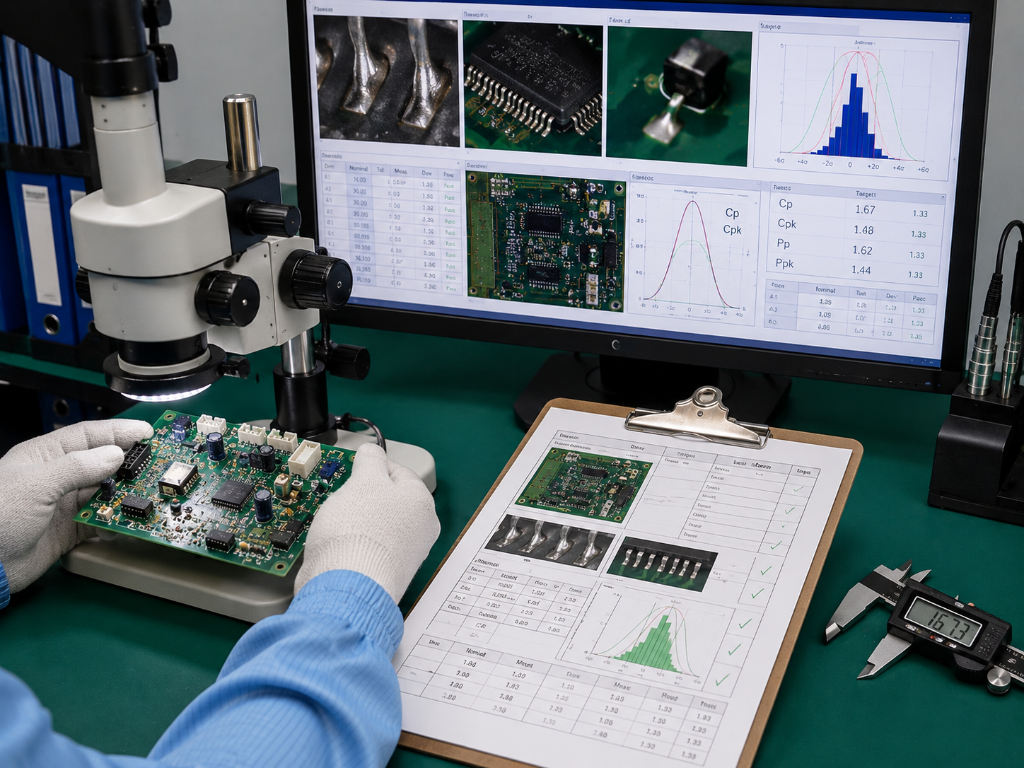
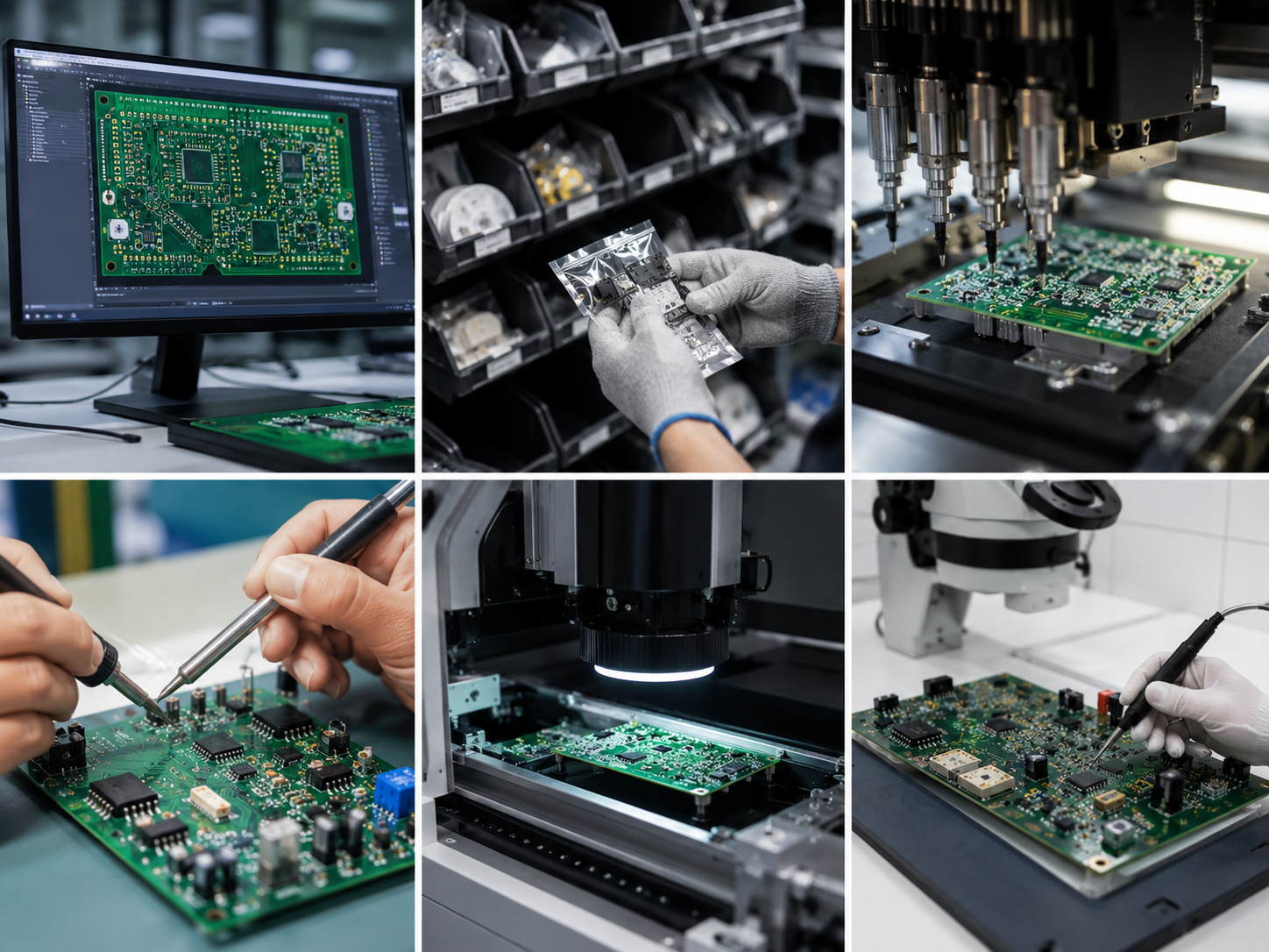
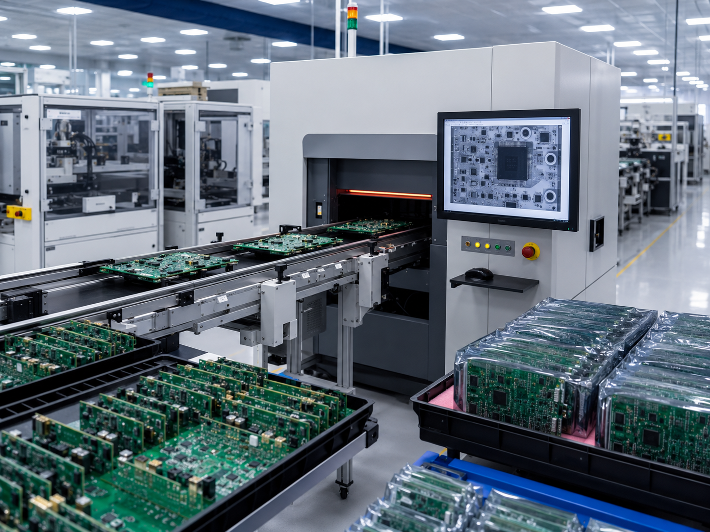
High-reliability through-hole PCB assemblies, backed up by the strict process control required: all board will receive AI-enhanced AOI inspections, and our standard production runs also provide X-ray examination to confirm correct via fill.
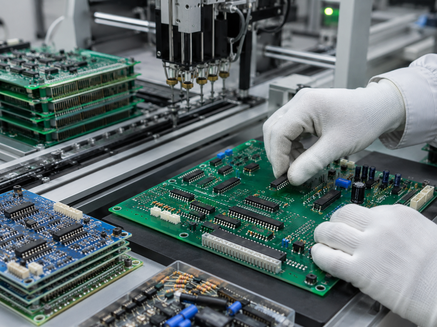
PCBark’s DIP assembly expertise spans every stage of through-hole and dual in-line package production – from the single piece DIP prototpe up to the massive multiple technology run. PCBs are assembled with components up to 40 pin package DIPs and the passives like axial and radial leaded through-hole connectors and big boy parts that SMT can’t take. If you’re trying to assemble a high technology complex mixed boards with a large quantity of DIPs on board PCBark’s specialty for selective solder is essential.
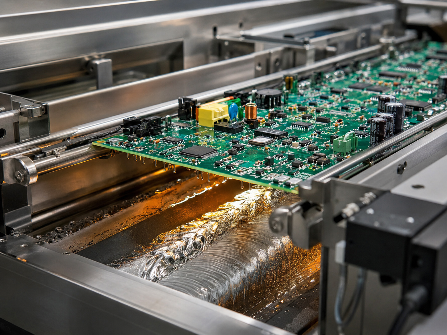
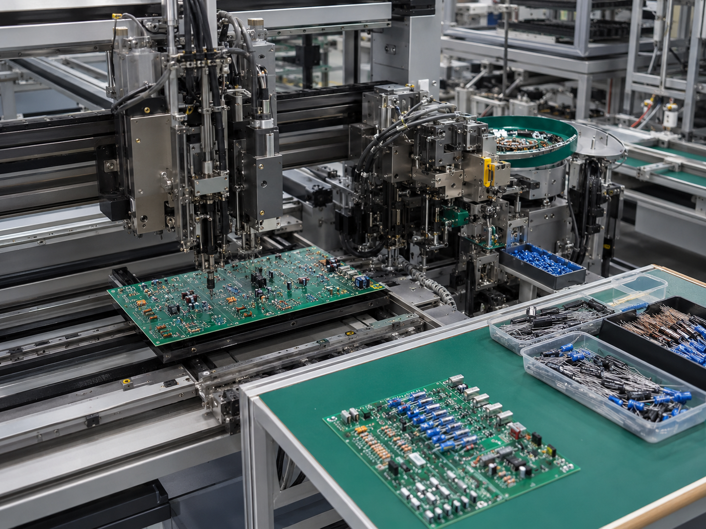
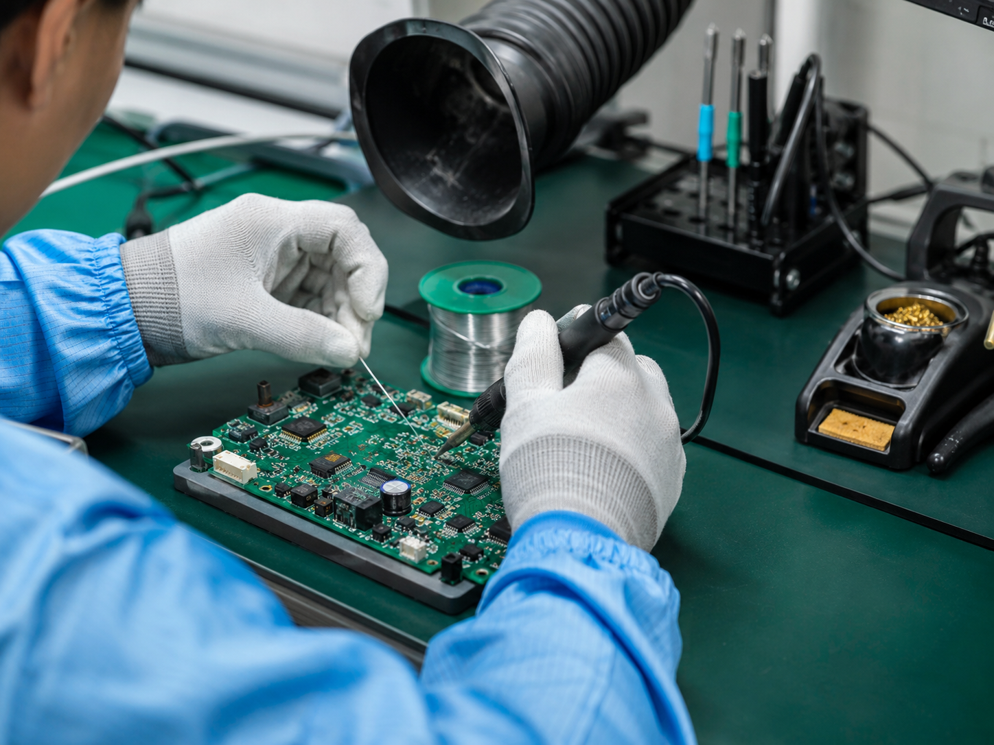
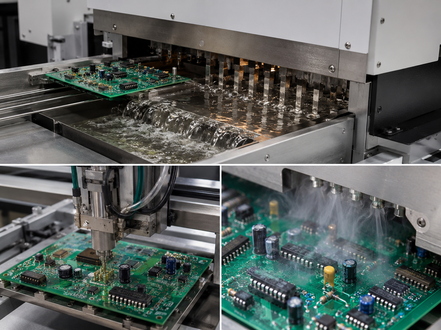
Our through-hole assembly services cover every circuit board assembly configuration: automated through hole assembly using high-speed installation of through-hole components at 33,000 CPH for axial component placement, wave soldering systems for standard THT runs, and manual soldering for large components requiring precision hand placement. PCBark’s soldering machine lineup handles automated wave soldering and nozzle selective systems to meet the quality standards required for high-quality through-hole PCB assemblies. All PCB manufacturing operations follow the highest quality standards per IPC-A-610, with electronics manufacturing services teams verifying component placement accuracy on every batch. Large components — including axial leaded components and through-hole mounting connectors — are processed with the same soldering and wave soldering process controls that govern all thru-hole PCB assembly work at PCBark.
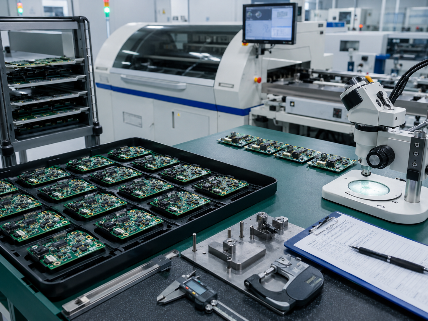
OPTICAL_INSPECTION_UNIT
01
DIP Assembly
Single-layer to 20-layer boards; DIP packages up to 40 pins; automated + manual insertion
02
Wave Soldering
Lead-free SAC305 and SnPb; bath temperature 250°C–270°C controlled; dual-wave capability for mixed SMT+THT boards
03
Selective Soldering
Nozzle-based selective soldering for mixed-technology PCB assemblies where SMT components on the solder side cannot be wave-exposed.
04
Axial & Radial Insertion
Automated axial insertion at 33,000 CPH; radial lead forming and insertion; manual through-hole for odd-form components
05
Hand Soldering
IPC J-STD-001 certified hand soldering stations; selective touch-up and repair; lead-free and tin-lead processes
06
PCB Inspection
AI-enhanced AOI on every board; X-ray barrel fill verification for Class III; in-circuit test (ICT); functional test
07
IPC Certification
IPC-A-610 Class II and Class III — both levels certified and available per order requirements
08
Component Types
Axial/radial passives; DIP ICs; TO-style transistors; large electrolytics; power transformers; edge connectors
The single most likely failure to occur in DIP assembly is the mixed-technology wave solder: if a mixed-tech board goes through the full solder wave covering the entire solder side of the board, the SMT components on that side of the PCB will be bathed in temperatures up to 250C +. In the challenging arena of DIP assembly, nothing poses a bigger challenge than the mixed-tech PCB – some SMT components are on one side of the board and others are mixed through-holes and DIP-components. Waving both sides leaves the SMT chips at risk from 250 C+ solder bath temperatures; that the PCBark program applies special nozzle programs designed specifically for each assembly to selectively place SMT components.
Through-Hole vs SMT vs Mixed Technology: The Selection Matrix
The ultimate PCBA design choice boils down to one single question – Which assembly technology works best for your mechanical and electrical objectives? We take the decision and model the trade-offs in the PCBark THT/DIP Technology Selection Matrix which is a 9-factor comparison for you to use as a DFM Gate review point before your next design release.
Every technology selection is a trade-off of mechanical capabilities, board density and the economics of the board, we help you quantify these trade-offs instead of using High /Med/ Low.
Poor through-hole assembly management is responsible for the bulk of through-hole field failures; cracked solder, unfilled barrels, cold solder joints caused by poor thermal profiles and skewed component leads that pass visual but are unstable in vibration. Every one of these failure paths is engineered out of the process during the initial DFM review your previous EMS partner likely missed, on the front end of PCBark’s complete turnkey DIP assembly solution.
01
DFM Review, 24hr Turnaround
Submit Gerber files + BOM. Engineers check hole-to-lead ratio (optimal: lead diameter + 0.4mm per IPC 2222), pad-to-hole relationship, component clearances for wave/selective nozzle path, and conformal coating requirements. Report delivered within 24 hours.
Turnaround 24 Hours
Standard IPC 2222
02
Component Sourcing & BOM Verification
Authorized distributor sourcing only. Counterfeit screening per component lot. RoHS and leaded process confirmed against BOM specifications. Every DIP package verified against land pattern before insertion.
Source Authorized Only
Verification 100% Pre-insertion
03
Automated Component Insertion
Axial and radial components: automated insertion at 33,000 CPH (Universal RAD 5 lines). DIP packages and connector headers: programmed semi-automatic and manual insertion per placement data. Lead cutting and clinching per IPC-A-610.
Speed 33,000 CPH
System Universal RAD 5
04
Wave Soldering / Selective Soldering
Standard THT assemblies: dual-wave lead-free SAC305 at 250°C–270°C bath. Mixed SMT+THT boards: selective soldering nozzle program protects SMT components while soldering through-hole pads. Nitrogen inerting for fine-pitch.
Bath Temp 250°C–270°C
Alloy SAC305 / SnPb
05
AI-Enhanced AOI Inspection
Every board scanned for solder bridge, insufficient solder, lead protrusion out of tolerance, and component misalignment. AI-enhanced pattern recognition flags anomalies below human visual threshold.
Coverage 100% Scanned
Engine AI Pattern Recognition
06
X-Ray Barrel Fill Verification
IPC-A-610 Class III assemblies: 100% X-ray on every batch to verify ≥75% barrel fill with no exceptions. Class II assemblies: first-article X-ray as standard. Results archived with FAI report package.
Class III 100% Batch Test
Target ≥75% Barrel Fill
07
Electrical Test & Functional Verification
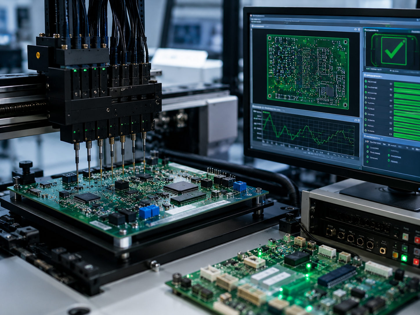
In-circuit test (ICT), flying probe, or functional test per board design. Test coverage mapped to your BOM. Results included in delivery package.
Methods ICT / Flying Probe
Mapping BOM Coverage
08
IPC-A-610 Sign-Off & FAI Report
First article inspection (FAI) report with dimensional measurements, solder joint records, and IPC-A-610 Class II or III certificate. Cpk/Ppk process capability data on request. This is the documentation your quality audit team needs.
Report Full FAI Package
Cert Class II / III
Applications: Where Through-Hole Is Non-Negotiable
Through-hole and DIP assembly isn’t a legacy holdover—it’s the specification requirement for product categories where SMT’s surface adhesion can’t meet working loads.
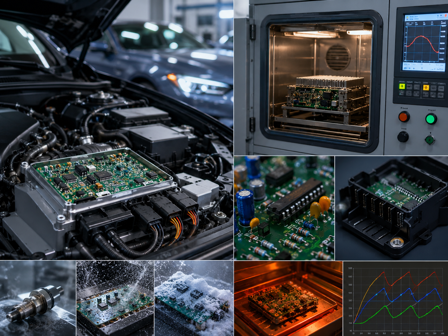
AEC-Q200 qualification; engine-bay thermal cycling; DIP components in power modules.
STDAEC-Q200, ISO 26262
Industrial Control
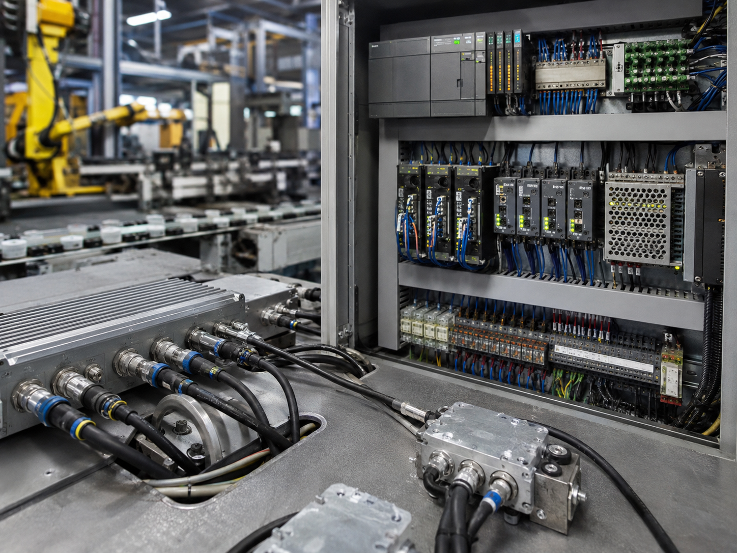
PLCs and servo interfaces operating 24/7 in high-vibration factory environments.
STDIEC 61508 SIL 2/3
Medical Devices
Life-critical hardware where mechanical security of through-hole is a prerequisite.
STDISO 13485, IEC 60601
Power & Energy
High-current transformers, large electrolytic capacitors, power transistors.
STDIPC-A-610 Class III, UL
I/O Interfaces
Connectors subject to repeated plug-in/removal needing extreme mechanical robustness.
STDIPC-A-610 Class II/III
[ENGINEERING_SUMMARY] If the design requires mechanical anchorage beyond what a surface-mounted pad can provide, or the component body is too large for reflow, the answer is through-hole.
IPC-A-610 Quality Certifications & Standards
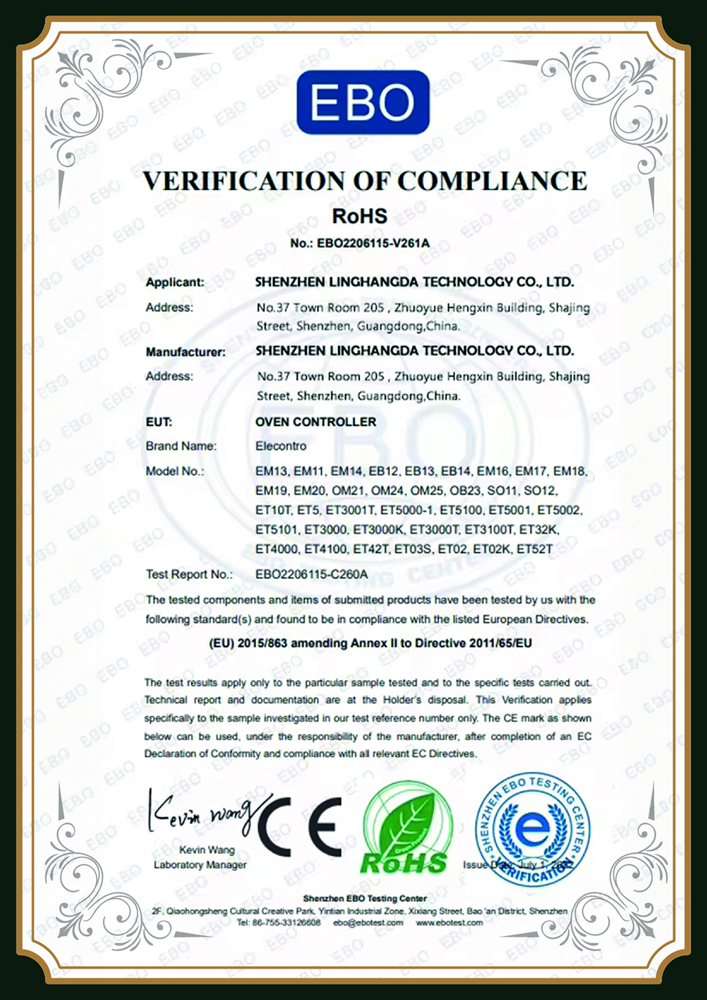
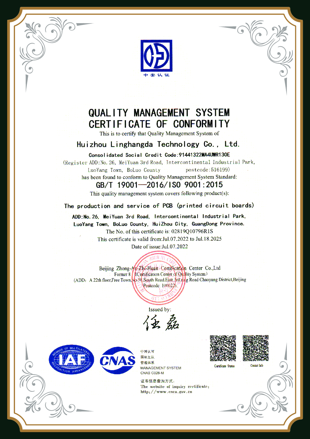
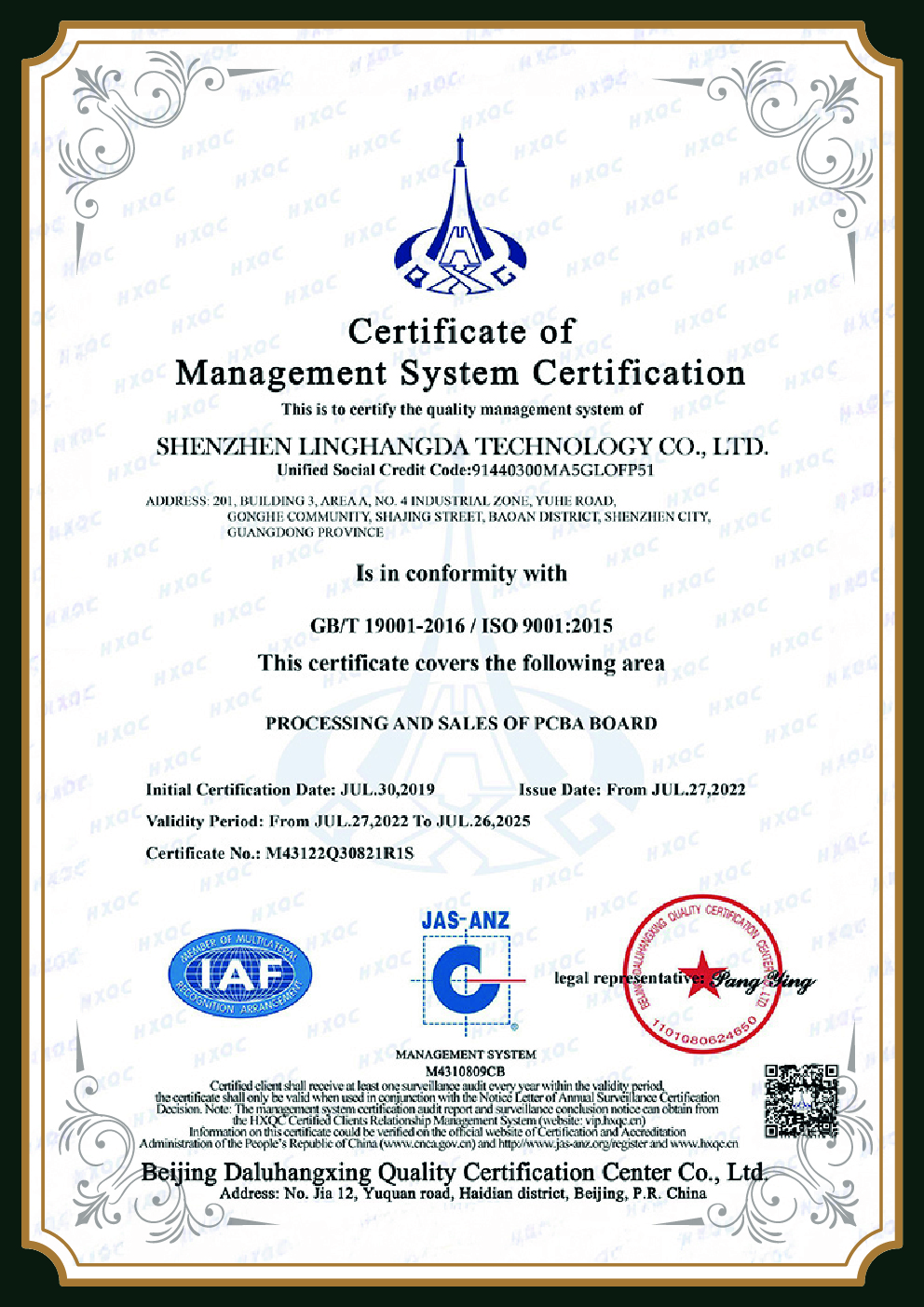
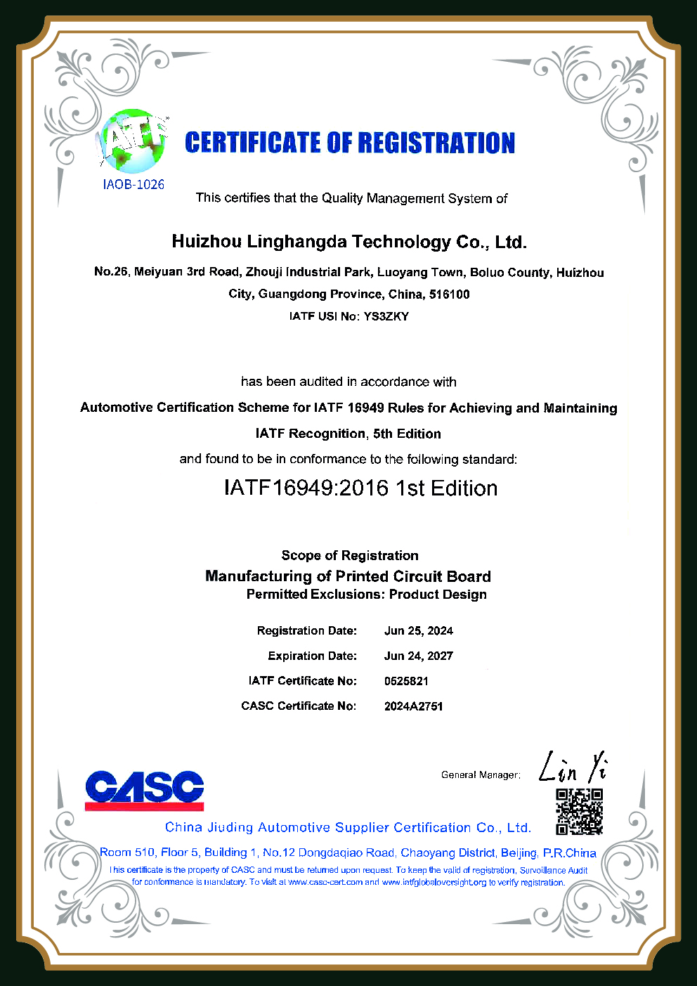
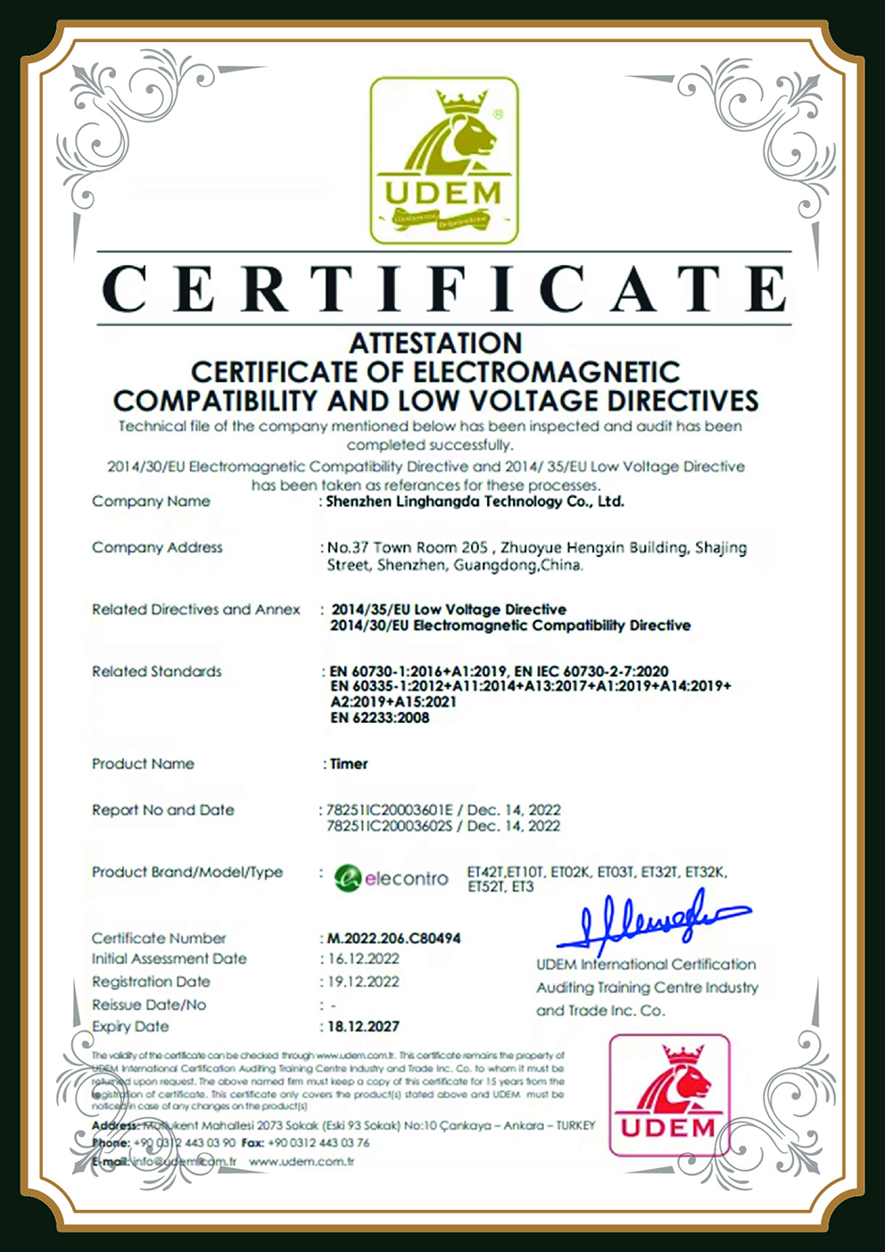
When a buyer audits a Chinese EMS supplier and the certification paperwork doesn’t materialize, that’s not a paperwork problem-it’s a quality system problem. PCBark holds IPC-A-610 Class II and Class III certification-both levels-and can produce the relevant inspection records for any order.
🔷
IPC-A-610 Class IIIHighest tier — zero-void specification
🔷
IPC-A-610 Class IIStandard commercial tier
📋
ISO 9001Quality management system
⚡
ULSafety standard
🌿
RoHSEU Directive compliant
🔬
J-STD-001Soldering requirements
The difference between Class II and Class III in through-hole assembly isn’t cosmetic. It translates directly into quantifiable production requirements that most EMS providers don’t meet for standard commercial orders:
IPC-A-610 Requirement
Class II (Standard)
Class III (PCBark Premium)
Barrel Fill (Standard)
≥75% minimum
≥75% — no exceptions on any supported hole
Barrel Fill (Exception — ≥14 leads)
50% minimum OR 1.2mm allowed
No exception — 75% on all
Circumferential Wetting
≥180° on destination side
≥270° on destination side
Voids in Barrel
1 void in up to 5% of holes allowed
Zero voids allowed
Plating Thickness
0.8 mil minimum
1.0 mil minimum
Ionic Contamination
Not specified at Class II
<0.78 μg NaCl/cm² maximum
X-Ray Verification
First article only
100% per batch at PCBark
PCB Assembly Service: From Prototype to Production Runs
A common failure mode in PCB assembly procurement: the EMS provider that handles your prototype work doesn’t have the process discipline for production, or the production house can’t match the prototype quality. The through-hole PCB assembly service covers the full lifecycle-prototype DFM validation through high-volume production runs-with the same IPC-A-610 certification and the same engineering team.
No MOQ
Prototype from 1 unit, no NRE fees
$2–6
Per board at 10,000+ unit production
24hr
DFM review before first Gerber release
No MOQ policy verified via PCBark specification. Per-board cost range: industry benchmark for production volume THT assembly.
For electronics teams that iterate on hardware designs, the absence of a minimum order quantity means DFM validation runs don’t require artificial order padding. For mixed-technology and high-density projects, see our low volume PCB assembly service. Submit 5 boards for first-article review, incorporate the DFM findings, and scale directly to production volume-with PCBark’s engineering team holding continuity across both phases. Process parameters from your prototype run (selective solder program, wave bath profile, insertion sequence) are archived and reused for production, eliminating the re-qualification overhead that switching suppliers always triggers.
Production process qualification • Cpk/Ppk capability data • process sign-off
STAGE 03
Production (100+ units)
Full automation where applicable • batch X-ray for Class III • delivery with certificate of conformance
CONTINUITY
All steps
Same engineering team, same process records, same IPC level certification
The honest deal in PCB assembly procurement is this: SMT wins on density and volume economies, but through-hole wins on mechanical strength and reliability at any order quantity. Economic production run figures explain exactly why hybrid or pure through-hole PCB assemblies stay economically feasible: at 10,000+ unit volumes, DIP assembly projects cost between $2-6 per board – similar to hybrid projects when relay and power device probabilities mandate THT design regardless. This cost comparison only stays relevant when comparing equal reliability specs: choosing a Class II SMT line when your assembly specs call for Class III THT makes no sense.
PCBark is among the reliable PCB assembly service providers for expert through-hole PCB assembly services, through-hole PCBs, PCB assemblies, and printed circuit board assemblies of all complexities. Our PCB assembly solutions address every assembly method — from automated insertion to hand soldering — covering PCB components selection, PCB through-hole routing, and DFM for complex designs. Through-hole technology remains essential for PCB assembly needs where through-hole components provide the mechanical durability that surface-mount components cannot match on their own: the benefits of through-hole include structural integrity on the PCB board, reliable through-hole circuit connections under vibration, and long-term durability under thermal cycling. Our PCB assembly process uses electronics assembly best practices from initial design through production: design consultation with our engineers covers assembly technology choices, assembly method trade-offs, and PCB through-hole vs SMT decisions. PCB services at PCBark deliver reliable PCB assembly and electronics assembly for any project size — our PCB assembly solutions support your assembly needs from prototype PCB board builds to high-volume through-hole technology remains essential production programs. For a full list of PCB services, including thru-hole PCB assembly, through-hole circuit board assembly, and complex PCB projects with large components, request a free engineering consultation.
Select DIP assembly only when your parts need something a surface adhesion can’t provide: high-current connectors, large electrolytic capacitors, power transformers, board-mounted inductors, edge connectors at risk of frequent mating. DIP assembly is also compulsory for aerospace, defense and medical projects subject to IPC-A-610 Class III, AEC-Q200, MIL-SPEC vibration. In these circumstances, SMT joint adhesion doesn’t meet spec.
Do you support mixed SMT and DIP assembly on the same PCB?
Yes. PCBark receives mixed-technology PCB design layouts that call for assembled SMT components on the top side, with through-hole or DIP parts on the back. We selectively program the solder bath wave to soak through-hole or DIP pads while protecting the assembly’s SMT area from over exposure. This is our standard process for mixed-technology PCB assemblies.
What types of through-hole components can you assemble?
We assemble all method types of through-hole: axial and radial passives (resistors, capacitors, inductors), dual in-line package (DIP) ICs up to 40 pins, TO-style power transistors, MIL-spec edge connectors, pin headers and receptacles, large electrolytic capacitors, power transformers, potentiometers, switches and odd-form parts that need to be hand-placed. Automated and manual insertion also available.
How do you ensure soldering quality in through-hole PCB assembly?
Through-hole quality control at PCBark adheres to IPC-A-610 Rev H standards: all supported holes – 75% barrel fill (no exceptions to Class III), all features – AI-enhanced AOI, production runs: X-ray verification of barrel fill (Class III). Cpk/Ppk manufacturing data and measurements are available on every order, FAI reports available on every order. Batch IPC-A-610 certificates available on demand.
What is the difference between wave soldering and selective soldering for DIP assembly?
Wave applications use the entire solder side of a PCB as a single wave of hot flux. Selective applications program the single wave of flux to hit only the specific through-holes PCBark needs soldered. For maximum efficiency, wave applications run over all through-hole portions, selective applications run to specific parts only.
Do you offer both leaded and RoHS-compliant through-hole soldering?
Yes. PCBark offers a SAC305 lead-free (RoHS compliant) as well as a SnPb (Sn63/Pb37) leaded wave and selective soldering process. Defense and aerospace customers with legacy leaded requirements specify the SnPb process; customers requiring RoHS compliance, including commercial and European-market applications, specify the SAC305 process. Both processes are compliant with IPC J-STD-001 soldering requirements and are available with either an IPC-A-610 Class II or Class III inspection level.
Can I start with prototypes and scale to full production without switching suppliers?
Yes. PCBark doesn’t have an order minimum; you may start with a 1-unit DFM validation prototype and then scale to full production with the same process parameters, engineering team, and IPC-A-610 certification. Data from your prototype run is saved and will be used for subsequent production runs, reducing the overhead associated with re-qualification. One supplier from first prototype to production.
What is PCBark’s IPC-A-610 certification class for through-hole assembly?
Both IPC-A-610 Class II and Class III certifications are current and active. Class III is the highest class under the IPC-A-610 specification for aerospace, defense, and medical electronics. The Class III specification mandates 75% fill, zero voids in through-holes, 270 circumference on through-holes, and a 1.0 mil minimum thickness on the through-holes. Customers specify the required class for each order, and PCBark provides supporting documentation and certification.