
Get in touch with PCBark Company

PCBark · PCB Reverse Engineering
PCB Reverse Engineering Services — Recover Schematic, BOM & Gerber Under a Strict NDA
Send us a working or obsolete board and we’ll reverse engineer it back into manufacturable design data – fully populated schematic, bill of materials, netlist, and Gerbers – with your intellectual property protected from the very first email, not the project start date.
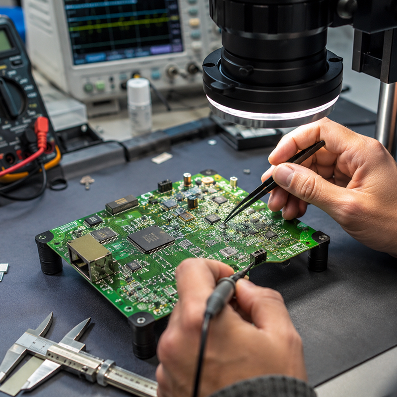
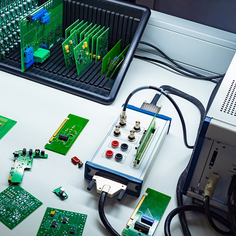
- 4 Outputs Schematic · BOM · Netlist · Gerber files
- Multi-layer 2 to 20+ layer boards, incl. buried/blind vias
- NDA-First Signed before any file or board is reviewed
- IPC-Class Re-fabricated to a declared IPC acceptance class
- Form-Fit-Function Verified against the original sample
16+ yrs
PCBark EMS heritage · 500,000 m²/yr capacity
Missing Your Original Design Data? Here’s How Reverse Engineering Gets It Back
For: Engineering · Procurement · Management
The situation
A line goes down. The board that runs it died, the original manufacturer is gone, and the design files left with them. You have one working sample and no schematic – and the part inside is obsolete, so there is nothing to simply re-order. This is the situation PCB reverse engineering exists to solve.
PCB reverse engineering is the process of taking a physical printed circuit board and reconstructing the design data needed to build it again – the schematic that shows how the circuit works, the bill of materials that lists every component, the netlist that captures each interconnection, and the Gerber files a fab house needs to make the board. When you reverse engineer a circuit board properly, you recover the ability to manufacture, repair, and improve a product whose documentation no longer exists – without redesigning it from a blank page.
PCBark treats this as a recovery service for boards you have the right to reproduce – your own legacy products, equipment you own and need to keep running, or designs you are authorized to recreate. That distinction is not a footnote; it is the first thing we settle, and it is covered in detail below.
Our Reverse Engineering Process & Deliverables — From Sample to Manufacturing Data
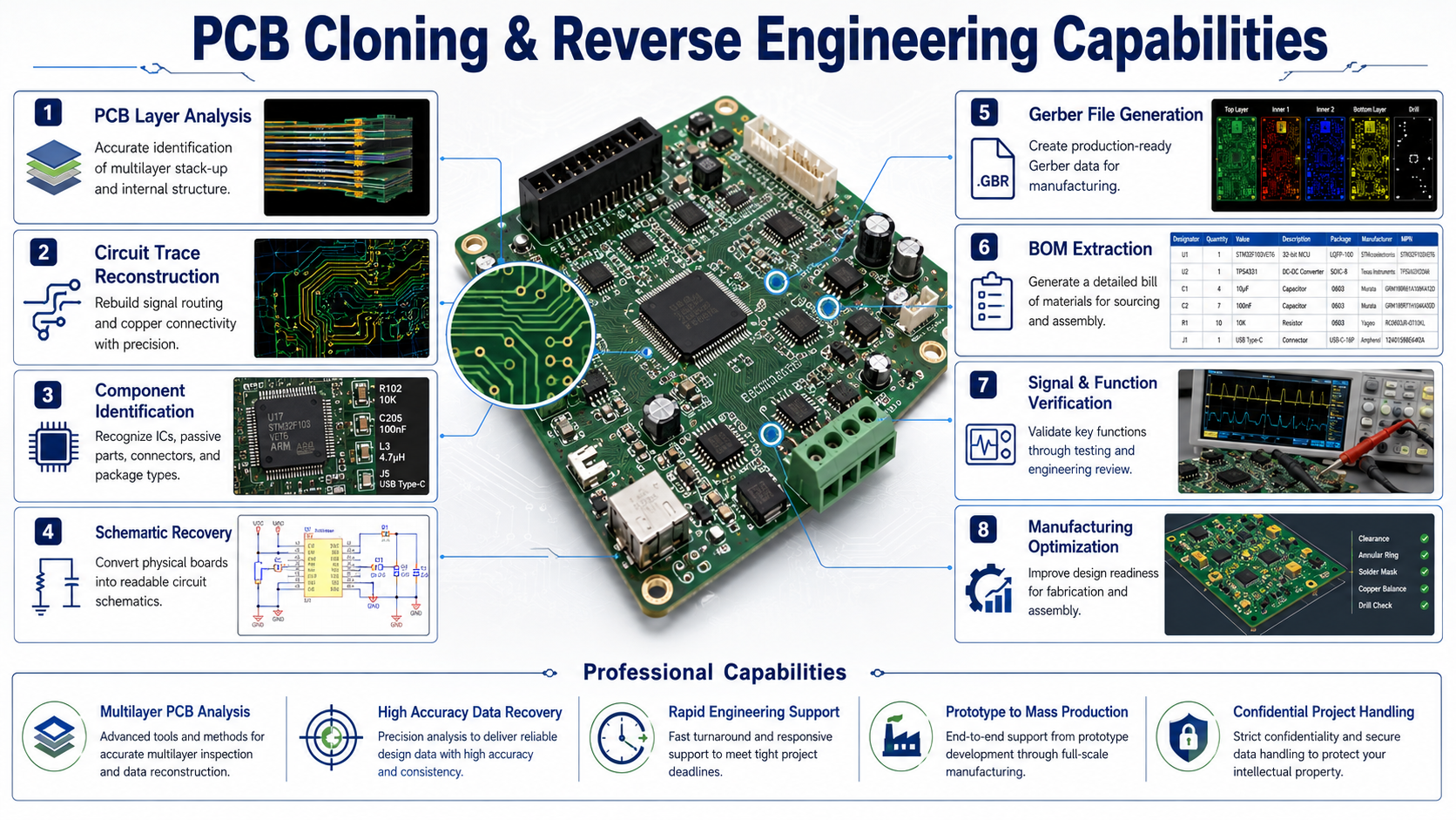
For: Engineering (Primary) · Procurement (Deliverable Match)Accuracy on a multi-layer board comes from method, not guesswork – no tracing by eye and hoping. We reverse engineer PCBs through a defined reverse engineering process where every layer, component, and connection is captured and then cross-checked against the physical sample. The reverse engineering techniques are matched to the board — from simple 2-layer cards to complex PCBs with buried vias and dense BGAs. Here is the path your board takes:
The Process
STEP 01
High-Resolution Scan
The bare and populated board are imaged at high resolution with a flatbed scanner and microscope to capture silkscreen, solder mask, pads, traces, and IC part numbers.
STEP 02
X-Ray / CT Imaging
X-ray and CT scanning reveal internal layers, vias, and connections under BGAs that no surface photo can show — essential for complex, multi-layer PCBs.
STEP 03
Netlist Extraction
Every interconnection is mapped into a netlist, layer by layer, including power and ground planes, so the electrical structure is captured exactly.
STEP 04
Schematic Capture
The netlist and component data are turned into a clean, readable schematic in CAD — the human-readable design that explains how the circuit works.
STEP 05
BOM Extraction
Every component is identified — value, footprint, and IC part number — and compiled into a bill of materials, with obsolete parts flagged for substitution.
STEP 06
Gerber & Layout
The PCB layout is rebuilt and exported as Gerber files and CAD design files, matching the original’s form, fit, and function.
STEP 07
Verification
A prototype is fabricated and checked with flying-probe and functional testing against your original sample before the data is released.
Deliverables
What You Receive
Schematic
Editable circuit diagram in standard EDA/CAD format showing the full design.
Bill of Materials (BOM)
Complete component list with values, footprints, and obsolescence notes.
Netlist
Full interconnection map for the printed circuit board, ready for re-layout.
Gerber Files + CAD
Fabrication-ready Gerber data and native design files for immediate manufacturing.
Engineering Note — Why X-Ray Matters on Multi-Layer Boards
On a 2-layer board, surface scans and careful tracing can recover most of the design. The difficulty scales with the number of PCB layers: an 8- or 12-layer board hides most of its interconnection on internal layers, and signals routed under a BGA are invisible to any optical method. Non-destructive X-ray and X-ray tomography — the same image-processing methods used in peer-reviewed PCB inspection research — let us read those buried vias, recover the layer stack-up, and map the inner layers of the PCB without destroying your only sample. IC part numbers are confirmed against manufacturer datasheets, and the recovered schematic and layout are cross-checked so the original design can be reused with confidence. Where a value genuinely cannot be read (for example, a laser-marked passive with no readable code), we tell you exactly which net it sits on rather than inventing a number. Honest boundaries are part of an accurate netlist.
Reverse Engineering, Done Legally — Strict NDA & IP-Ownership Verification
For: Procurement · Management (Legal & Risk)Most reverse engineering pages stay silent on the one question buyers actually lose sleep over: is this legal, and will my design leak? We put it first. Reverse engineering is a well-established, lawful practice when it is used for interoperability, repair, maintenance, and recovering data for products you own or are authorized to reproduce — a principle long recognized in intellectual property law. It crosses a line when it is used to copy someone else’s protected design, firmware, or branding. We work only on the right side of that line, and we verify it before we begin.
The risk competitors miss
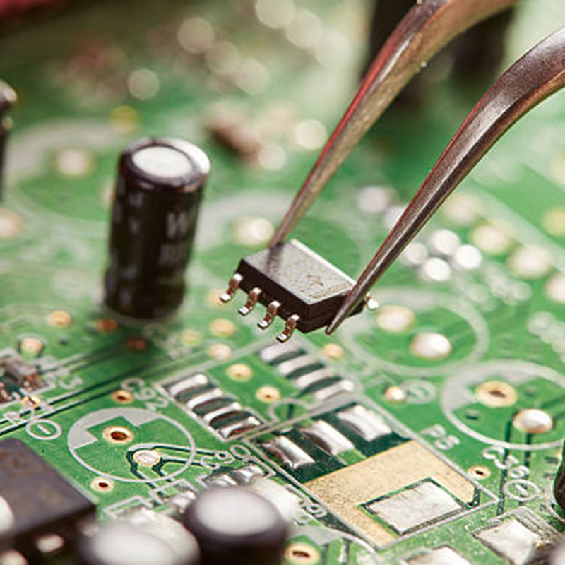
Here is the part competitors miss: the largest confidentiality risk in this whole process is not the workshop — it is the quoting stage. Buyers routinely email full Gerbers and BOMs to a dozen shops just to get a price, handing out their entire design before a single agreement exists. We close that gap:
How we close the gap
01
NDA Before Files
A mutual NDA is signed before you send a board or upload any design data — including for the quote.
02
Ownership / Authorization Check
PCBark confirms you own the board or are authorized to reproduce it. Requests to copy third-party protected IP are declined.
03
Controlled Handling
Your sample and data are access-restricted to the assigned engineers — not shared across an open quoting pool.
04
Return & Retention Terms
Boards and files are returned or securely retained under the terms you agree to — your call, in writing.
Before you request any quote — from anyone
Before you request any quote — from anyone
When inquiring, be sure to ask: has your NDA been signed? Who within your organization will be authorized to view my files? What’s your company’s verification process to prove I own the design? Any supplier that wants to peek at your Gerbers before any commitment is putting your sensitive intellectual property at risk; when you do business with PCBark, the NDA comes first.
Reverse Engineering vs. PCB Clone vs. PCB Copy — Which Service Do You Need?
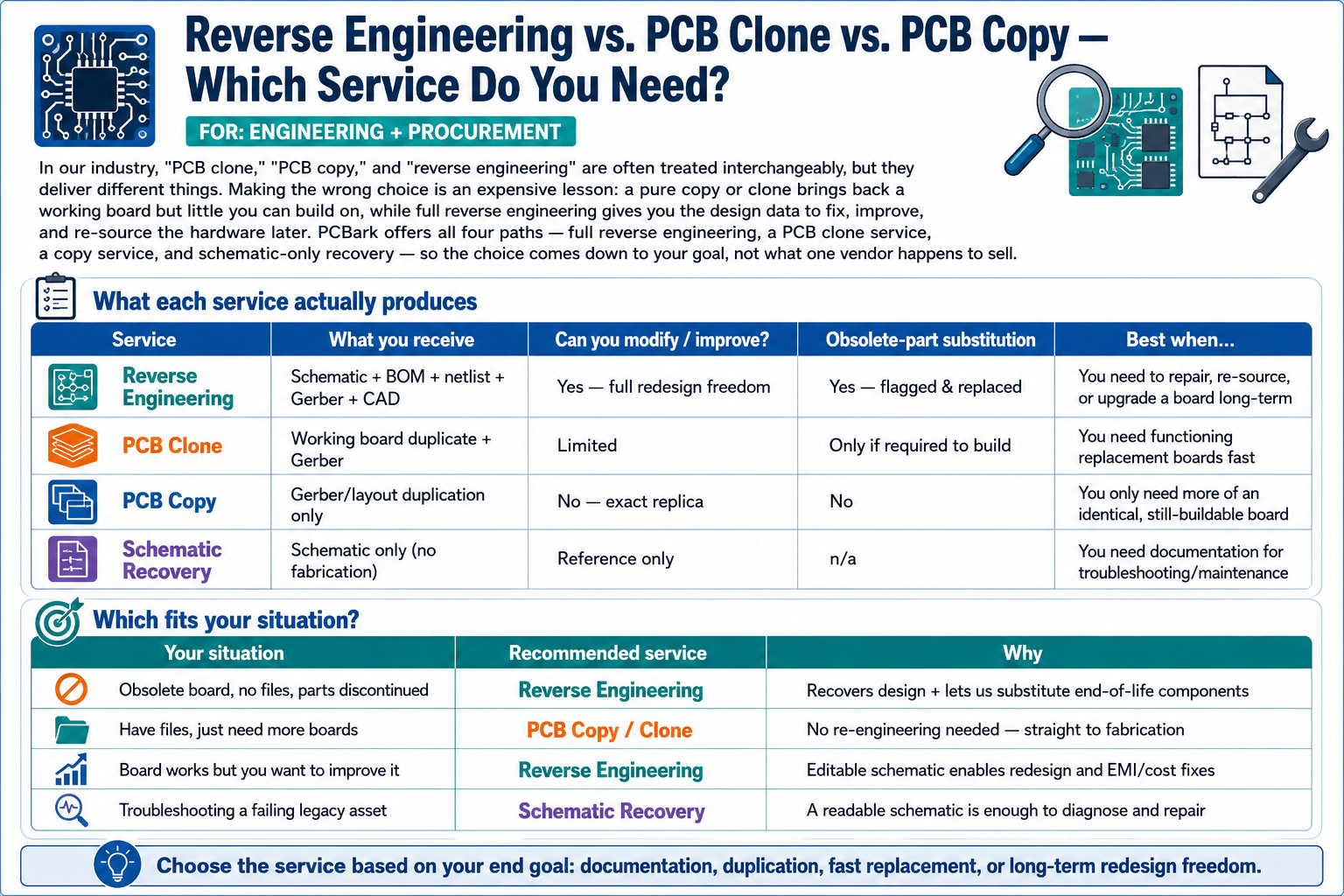
For: Engineering + ProcurementIn our industry, “PCB clone,” “PCB copy,” and “reverse engineering” are often treated interchangeably, but they deliver different things. Making the wrong choice is an expensive lesson: a pure copy or clone brings back a working board but little you can build on, while full reverse engineering gives you the design data to fix, improve, and re-source the hardware later. PCBark offers all four paths — full reverse engineering, a PCB clone service, a copy service, and schematic-only recovery — so the choice comes down to your goal, not what one vendor happens to sell. The table below maps what each service actually produces:
Service comparison
| Service | What you receive | Can you modify / improve? | Obsolete-part substitution | Best when… |
|---|---|---|---|---|
| Reverse Engineering | Schematic + BOM + netlist + Gerber + CAD | Yes — full redesign freedom | Yes — flagged & replaced | You need to repair, re-source, or upgrade a board long-term |
| PCB Clone | Working board duplicate + Gerber | Limited | Only if required to build | You need functioning replacement boards fast |
| PCB Copy | Gerber/layout duplication only | No — exact replica | No | You only need more of an identical, still-buildable board |
| Schematic Recovery | Schematic only (no fabrication) | Reference only | n/a | You need documentation for troubleshooting/maintenance |
Which fits your situation?
| Your situation | Recommended service | Why |
|---|---|---|
| Obsolete board, no files, parts discontinued | Reverse Engineering | Recovers design + lets us substitute end-of-life components |
| Have files, just need more boards | PCB Copy / Clone | No re-engineering needed — straight to fabrication |
| Board works but you want to improve it | Reverse Engineering | Editable schematic enables redesign and EMI/cost fixes |
| Troubleshooting a failing legacy asset | Schematic Recovery | A readable schematic is enough to diagnose and repair |
Not sure which path?
Get a free scoping call
Not sure which path fits your board? Get a free scoping call
Where Reverse Engineering Pays Off — Obsolescence, Repair & Legacy System Support
For: Management (ROI) · Engineering (Validation)The strongest argument for reverse engineering is the one most cost objections miss: when a board is obsolete, there is no “just buy a new one.” The original is discontinued and no drop-in substitute exists. So the real comparison is not reverse engineering versus a new board — it is reverse engineering versus a production line that stays down or a product you can no longer ship.
Component obsolescence is not rare. Independent lifecycle data indicates a large share of electronic components reach end-of-life without formal notice, while component lifecycles have compressed from decades toward only a few years — squeezing any product built to run for ten or twenty. In aerospace, medical, and industrial equipment especially, one unsupported board can strand an entire asset indefinitely.
$10K–$500K+
Typical cost of one hour of unplanned downtime when a legacy control board fails and no spare or design data exists — the loss reverse engineering is meant to prevent.
Industry estimates from manufacturing operations data, 2024 (Aberdeen / ABB / Siemens-ISM). Figures vary widely by industry and are provided as context, not a PCBark measurement.
Reverse engineering also recovers value well beyond the immediate repair. Once the schematic and BOM exist, you can re-source obsolete parts, improve the original PCB design to fix its weak points (thermal, EMI, or poor layout), and qualify a second source for fabrication and PCB assembly — turning a one-off rescue into a durable, cost-effective supply position for a legacy product.
Decision comparison
Reverse Engineering vs. Full Redesign From Scratch
| Dimension | Reverse Engineering | Redesign From Scratch |
|---|---|---|
| Source data needed | Physical sample only | Full requirements + new design |
| Form / fit / function | 1:1 match to proven original | Must be re-validated |
| Engineering effort | Days to a few weeks (typical, industry) | Weeks to many months |
| Risk | Built on a field-proven design | New design + new bugs |
These ranges reflect general industry experience for professional multi-layer work and depend on layer and component count; they are not PCBark-specific commitments.
Obsolescence risk
Request an obsolescence-risk review
Worried a critical board is about to go end-of-life? Request an obsolescence-risk review
Turnaround, Pricing Factors & Your Quote — A Procurement Guide
For: Procurement · Management (Budget)
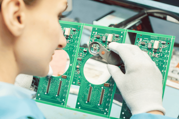
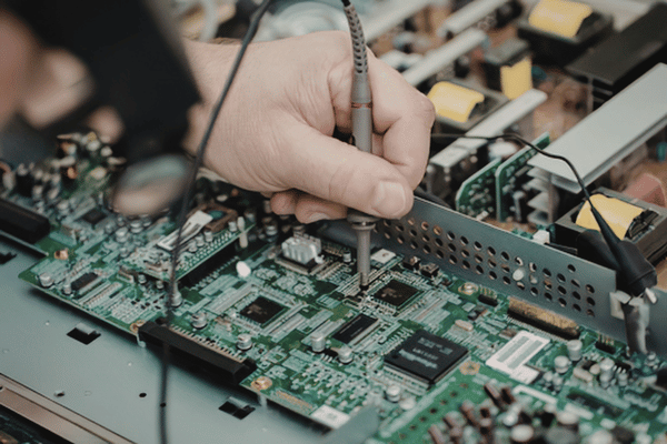
There is no single price for reverse engineering, and any provider quoting a flat number before seeing your board is guessing. What you pay and how long it takes are driven by a handful of measurable factors about the board itself. Knowing them lets you scope your project — and your budget — realistically before you ask for a quote.
Cost & lead-time factors
What actually drives your quote
Your reverse engineering cost and turnaround scale with these measurable factors about the board itself:
01
Board layers
A 2-layer design is far simpler to restore than a 16-layer one.
02
Component density
The number and density of components, including fine-pitch BGAs that require X-ray.
03
Board condition
A clean working sample versus a damaged one.
04
Deliverable depth
Schematic only versus full schematic + BOM + Gerber + verified prototype.
05
IPC acceptance class
The IPC acceptance class you need the rebuilt board fabricated to.
Share these and we can scope realistically.
Since every board is unique, we quote each project individually after receiving your sample for evaluation under non-disclosure agreement (NDA)-no blanket rate cards here. Just give us the layers, approximate number of components and the type of documents required, and we will issue a clear scope with a timeline estimate.
Scope your project
Request a Custom Quote & Lead Time
Ready to scope your board?
Accuracy, Verification & Standards — How We Prove the Board Is Right
For: Procurement (Certs) · Engineering (Standards Fit)Restored designs are only useful if they are accurate. Here’s how PCBark delivers something much more valuable than an estimate: We thoroughly test the newly fabricated board to confirm that it exactly matches the original prior to turning over the files. Each restored design is electrically verified and undergoes full functional testing while the physical board is fabricated to the stated IPC acceptability standard.
Verification Spine
The extracted netlist is checked against the physical board with flying-probe testing — the same PCB inspection discipline we apply in volume production — confirming every interconnection node-for-node. A prototype is then built and put through functional testing against your original sample — the same form, fit, and function. Fabrication follows recognized IPC acceptability and qualification standards, such as IPC-A-600 for board acceptance and IPC-6012 for rigid board performance, so “we verified it” means a defined, inspectable standard — not a sales adjective.
Standards & methods applied
ISO 9001
Quality management system*
IPC-A-600
Board acceptability
IPC-6012
Rigid PCB performance
Flying-Probe
Netlist verification
Functional Test
Against original sample
*Specific certificates and acceptance classes are indicative of the expertise and general practices employed by PCBark. The specific content, scope and number of applicable certificates would be confirmed in your signed agreement.
Compliance posture
Request our NDA & sample compliance documentation
Need to see our compliance posture first? Request our NDA & sample compliance documentation
Reverse Engineering Toolset
Scope Your Project Before You Request a Quote
Four interactive tools to identify the right service, estimate complexity, gauge obsolescence risk, and confirm you’re ready to proceed — all before you send a single file.
01
PCB RE Service Selector
Answer four questions and get pointed to the right service — reverse engineering, clone, copy, or schematic recovery.
Launch Tool
02
RE Project Scoping Estimator
Gauge how involved your reverse-engineering project is and build a clean quote request in the process.
Launch Tool
03
PCB Obsolescence Risk Calculator
Score how urgently a legacy board should be reverse engineered as a continuity safeguard.
Launch Tool
04
NDA & IP Readiness Checklist
Confirm you can proceed cleanly before sending files — PCBark signs a mutual NDA first, every time.
Launch Tool
Frequently Asked Questions
PCB Reverse Engineering FAQ
Is PCB reverse engineering legal?
Yes, when it is used for legitimate purposes — interoperability, repair, maintenance, and reproducing boards you own or are authorized to recreate. Reverse engineering for these reasons is a long-recognized and lawful practice in IP law, and it is the entire reason this service exists: keeping equipment you already own running after the original supplier and its files are gone. What is not legal is copying a third party’s protected design, firmware, or branding to compete with them. That is the line, and ownership or authorization is verified before any project starts.
Can you reverse engineer a PCB without the original schematic or design files?
That is exactly what this service is for. We work from the physical board alone — scanning, X-ray/CT imaging the internal layers, extracting the netlist, and rebuilding the schematic, BOM, and Gerber files from scratch. No original files are required.
How do you protect my IP and confidentiality?
A mutual NDA is signed before you send a board or any file — including for the quote, which is where most leaks happen. Your data is access-restricted to the assigned engineers, and boards and files are returned or securely retained under terms you set in writing.
Can you reverse engineer multi-layer or complex boards?
Yes. Multi-layer boards (commonly 4 to 20+ layers) are handled with X-ray and CT imaging to read internal layers, buried and blind vias, and connections under BGAs that surface scans cannot see. Where a specific value is physically unreadable, we identify the net it belongs to rather than guess a number.
What deliverables do I receive?
A complete schematic, a bill of materials (BOM) with obsolete parts flagged, a netlist, and fabrication-ready Gerber files plus native CAD design files. Optionally, a verified prototype fabricated to a declared IPC class.
What’s the difference between reverse engineering, PCB clone, and PCB copy?
Reverse engineering recovers the full editable design (schematic + BOM + netlist + Gerber) so you can repair, re-source, and improve. A PCB clone produces working duplicate boards. A PCB copy duplicates the layout only. See the comparison table above to match the service to your goal.
How long does PCB reverse engineering take and what does it cost?
Both depend on layer count, component count and density, board condition, and which deliverables you need. We scope each project after reviewing your sample under NDA and return a clear lead-time and price estimate — we don’t quote a flat rate sight-unseen.
Do I need to send you the physical board?
Yes. The physical sample makes accurate multi-layer netlist extraction and verification possible; secure, NDA-covered handling is arranged first.
Start Your Recovery
Recover Your Board’s Design — Confidentially
Just send us the board, and we will return an all-inclusive package of documents: schematic, BOM, Netlist, and Gerber. All files remain under NDA until it is signed and you transmit your board samples to us.
Request a Quote
NDA-first · Files protected
![16-24 Layer PCB: Stackup, Lamination & Design Guide [2026]](https://pcbark.com/wp-content/uploads/2026/07/16-24-layer-pcb-guide-featured-2-150x150.png)


