
Get in touch with PCBark Company

ANY-LAYER HDI · SEQUENTIAL LAMINATION
Any-Layer HDI PCB Manufacturing — Sequential Lamination & Copper-Filled Microvias
If your fine-pitch BGA just quit fanning out on 1+N+1 HDI, then the issue is with your routing, not layout. PCBark provides any-layer HDI – where every layer is an interconnect-so we pack it all to meet the footprint that actually fits into your to-be-shipped product.
Request an Any-Layer HDI Quote
Specifications
Any-Layer / ELIC
Every layer interconnect, plus 1+N+1 to 3+N+3
~100 µm
Copper-filled microvia, 0.75:1 aspect ratio
75 µm
Line / space reach on advanced builds
Class 3
Built & inspected to IPC-6012 Class 3
30–40%
Typical board-area reduction vs conventional
16+ yrs
EMS experience, 500,000 m²/yr capacity
Technical Advantage
When Standard 1+N+1 HDI Runs Out of Routing Space
You know the story. Placement is ok, schematic is ok, but the thickest BGA won’t escape. The via passages in between balls have disappeared, and we are facing the only way to increase the number of layers; we’ll thicken and enlarge the board. Here HDI stops.
For an ELIC, however, there’s no wall. On a conventional multilayer PCB, connectivity goes to microvias on top and to buried vias within the core of the stack, but the rest of the routing must use the plated through-holes within the board’s body. A printed circuit board built on an any-layer stack-up does away with that limitation – rather than confining blind via connectivity to the build-up over a through-hole core, each dielectric layer has its own set of copper-filled, laser-drilled microvias.
Read moreShow less
Thus, any of those layers may connect to any adjacent layer. If stacked microvias are incorporated into an ELIC stack-up the connectivity may then be extended as high as the highest layer on the board stack. That is how we were able to route a 0.4mm-pitch chip into the test boards that an equivalent build-up including 2+N+2 could not close.
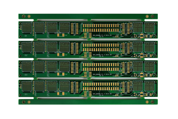
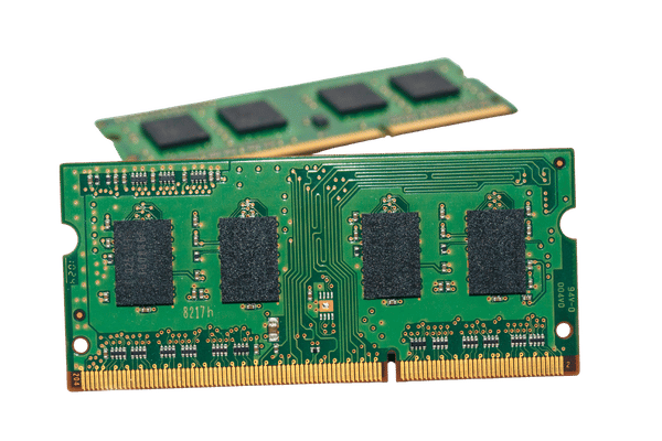
What the end user gets is reduced size and increased density. Since no particular layer is “off-limits,” traces can pass through the same layer 2 of 10 layers used by any-layer as they did on a 14 layer conventional design; designers can take a step down on overall layer count to reach that same number of connections; and can reduce the overall outline size by up to 40% over conventional board construction.
Read moreShow less
That space saving carries an admission price: processing. Any layer technology uses sequential laminations, and, according to one source close to the technology, any layer HDI is still considered an advanced, nonstandard technology that isn’t readily available by most PCB fabricators. PCBark does offer the capability.
01 / Capabilities
PCBark Any-Layer HDI Capabilities — Stackups & Structures
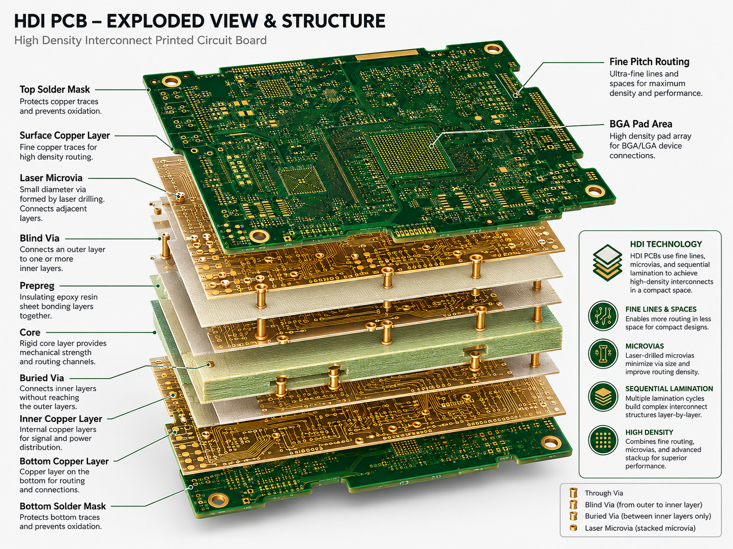
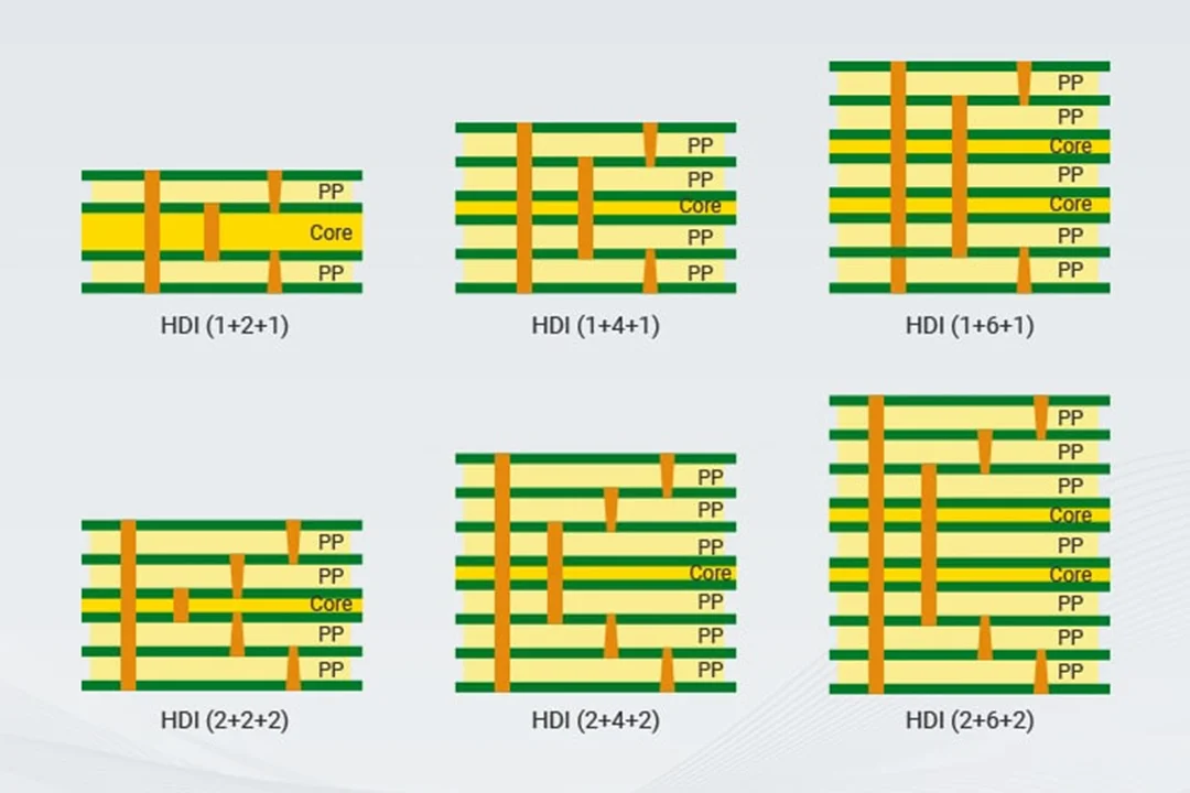
Most HDI does not use any-layer, and an honest capabilities page must show you the right HDI for the application; usually, we are searching for the cheapest board which is possible to rout out of it. Here it shows how to map a typical structure to the appropriate place of its application; basically the ladder can be climbed only until the next level does not supply enough routing channels any more.
| Structure | Microvia build-up | Routes well for | When to step up |
|---|---|---|---|
| 1+N+1 | 1 microvia layer each side over a core | Single dense BGA, >0.5 mm pitch, moderate I/O | Escape channels tight on one package |
| 2+N+2 | 2 microvia layers each side | 0.4–0.5 mm pitch BGA, higher I/O | Stacked packages, multiple dense parts |
| 3+N+3 | 3 microvia layers each side | Very high I/O, multi-BGA boards | Via channels still exhausted, area constrained |
| Any-layer (ELIC) | Every layer is an interconnect layer | Sub-0.4 mm pitch, max density, smallest outline | This is the ceiling — full routing freedom |
02 / Capability Window
Engineering Capability Window
Any-layer boards are built around near 100 micron copper filled microvias at 0.75:1 aspect ratios-the one aspect ratio our plating window allows and IPC-2226’s reference for its “reliable target” rather than its more generous 1:1 max — plus fine-line geometries down to 75 µm line width/spacing in our advanced constructions, and 75–150 µm actual completed microvia diameters on standard boards and even smaller for specialty builds.
Read moreShow less
Microvias themselves are produced by laser drilling across layers, then plated and via-filled with copper so the next layer’s capture pad lands flush. Layer-to-layer registration is the biggest contributor to any-layer cost — or rather the biggest risk. Each lamination cycle has its risk of the stack migrating, hence our work with customers to control prepreg flow alongside lamination cycles. Shorter trace lengths in tighter feature geometry also improve signal integrity alongside the density gain, which is the other half of the miniaturization story. This is how our team approaches building any-layer circuits; your specific performance capabilities are subject to copper weight, dielectric, and layer counts, all determined with our DFM engineers prior to production tooling.
| Parameter | Capability | Reference |
|---|---|---|
| Interconnect structures | 1+N+1, 2+N+2, 3+N+3, any-layer / ELIC | IPC-2226 design tiers |
| Microvia | Copper-filled, ~100 µm, aspect ratio 0.75:1 | IPC-2226 / IPC-6016 |
| Line / space | Down to ~75 µm on advanced builds | Confirmed at DFM |
| Via protection / fill | Copper-filled stacked & staggered microvia, via-in-pad | IPC-4761 |
| Reliability class | Built & inspected to IPC-6012 Class 3 | IPC-6012 |
| Assembly | Turnkey SMT, component sourcing, functional test | PCBark in-house |
Set against a through-hole circuit board, the any-layer board holds a finer line width and spacing because it relies on laser drilling its microvias rather than the mechanically drilled blind via and buried via spans a conventional board depends on. A mechanically drilled circuit board cannot place holes that small or that close, which is why the line width and spacing keep shrinking as the board area comes down.
Read more — notes for the shopShow less
Two side notes for the shop. We try to keep the sequential laminations and cycle count to a minimum and dictated by your build complexity – more lamination cycles mean more press ops, drills, plating, images, etc., so oversourcing an unnecessary any-layer board is a costly error on our part. In addition to managing those complexities, when routing under your BGA, microvias in pads are planarly flattened after fill so your soldermask and paste sit evenly; if you’re looking for routed density that’ll cause placement and assembly headache, feel free to do just that. Any-layer technology also pairs well with a rigid-flex design when the product has to fold, and managing the thermal management of Z-axis expansion matters once the stack gets tall — our design for manufacturing (DFM) team looks at these options early to avoid cost jumps later.
Any-Layer HDI vs Sequential 1+N+1 vs Through-Hole — The Data
High, Medium, and Low belong on a brochure, not on a board you have to sign off on. What follows is a rendering of a sample circuit design laid out in the context of three common construction types based on the considerations that truly drive your cost and time to market, not on a category level that oversimplifies the problem: the number of routing opportunities the board presents, the eventual size it needs to be, and the required cost to get there.
| Parameter | Through-hole multilayer | 1+N+1 HDI | Any-layer HDI |
|---|---|---|---|
| Min BGA pitch routable | ~0.8 mm | ~0.5 mm | ≤0.4 mm |
| Via type | Plated through-hole | Microvia outer + PTH core | Copper-filled microvia, every layer |
| Relative board area | Baseline (100%) | ~75–85% | ~60–70% |
| Layers for same fan-out | Highest | Lower | Lowest |
| Signal path length | Longest | Shorter | Shortest |
| Lamination cycles | 1 | 1–2 | 3+ (sequential) |
| Relative fab cost | Lowest | Moderate | Highest, offset by size & layer savings |
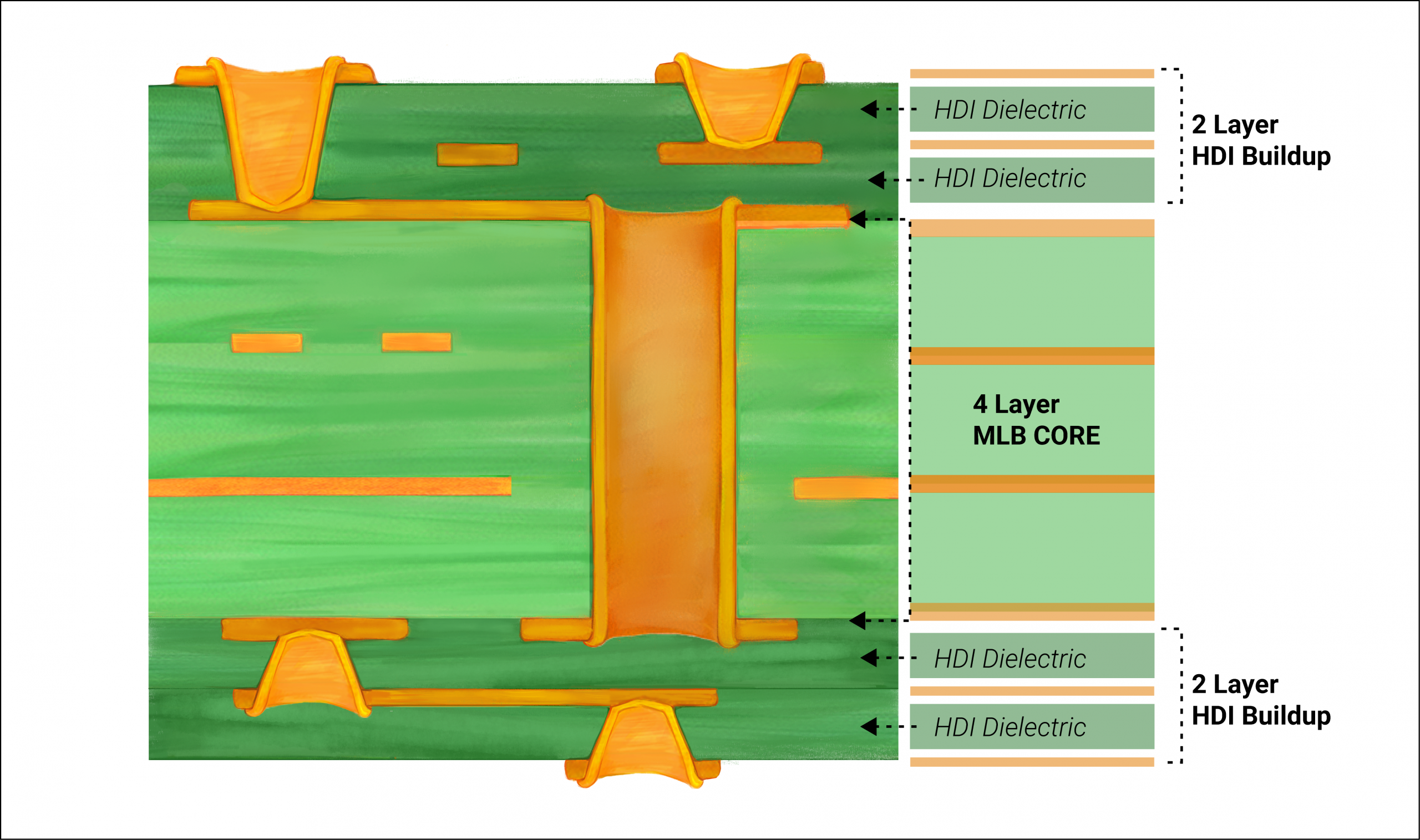
/// RENDER DATA
The cost truth in numbers: any-layer is the most expensive to fabricate due to repeating the sequential lamination sequence on each of the six sequential lamination stages, and figures show 6-layer HDI coming in around 30-50% above 4-layer simply for this reason.
Read moreShow less
This metric, however, misses the system trade. You save not just money but space by employing smaller form factors, reducing the required number of layers, and increasing assembly yield by laying vias in the pads of the intended component versus in direct opposition of those pads. For any product built within strict space requirements, a through-hole may appear cheaper initially than any-layer. However once you consider enclosure, required layers, and rework, through-hole may cost you more in the long run.
Customer Results: Footprint, I/O Density & Microvia Reliability
Any-layer makes sense when trying to address size, routing density and reliability:
Case Scenario 01
Fitting a sub-0.4 mm BGA into a wearable outline
In one instance a team developing a consumer product featuring a smartphone-class processor had to lay out 0.35-millimeter (mm) pitch components but were unable to successfully escape the routing through all of their 2+N+2 layers. By implementing an any-layer build, they were able to escape the routes across the entirety of the board, successfully bringing the design within physical parameters and not requiring additional layers.
≤0.4 mm
BGA pitch routed
~35%
Board-area reduction
0 added
Layer pairs vs prior stack

Case Scenario 02
Surviving thermal cycling without microvia separation
When faced with building an aerospace module, which, much like the implant required for a medical device, adheres to a similar high bar for reliability, the concern of the team was whether they would be able to prevent stacked microvias from failing under deep, severe thermal cycle testing. Many engineers struggle with ensuring controlled Z-axis thermal expansion as this is a real engineering challenge. This particular board build relied on copper-filled holes, a carefully controlled cycle count, the use of staggered through-holes where permitted, and via isolation per IPC-4761; it was also inspected according to IPC-6012 class 3.
Class 3
IPC-6012 build & inspection
Cu-filled
Microvia structure
IPC-4761
Via protection applied
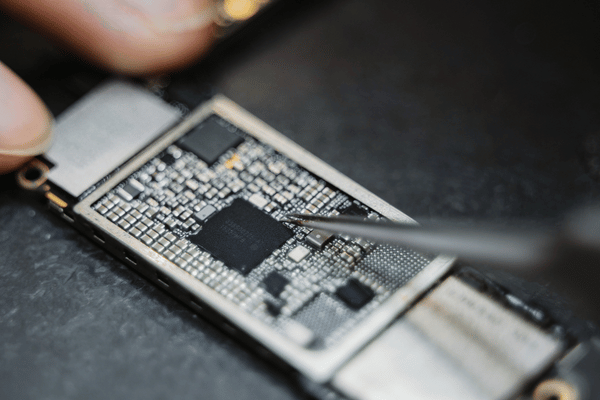
Case Scenario 03
Breaking out a high-pin-count FPGA
High I/O FPGA designs, long after the required layout is completed, continue to have insufficient via options on conventional layouts. Any-layer boards allot each level for fan-out design, thereby ensuring that the break-out routes remain intact and impedance controlled pairs continue on their intended path without being obstructed by via locations.
Any-layer
Full-stack fan-out
Z-axis
Stacked microvia routing
Controlled
Impedance pairs preserved

Quality Assurance
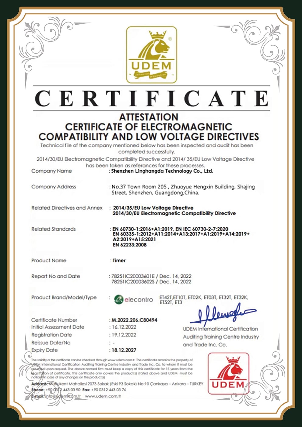
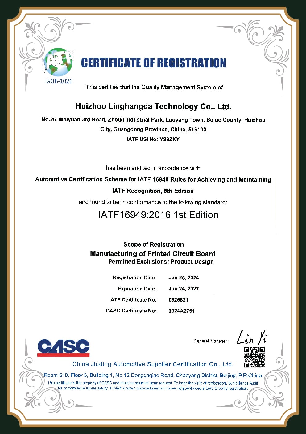
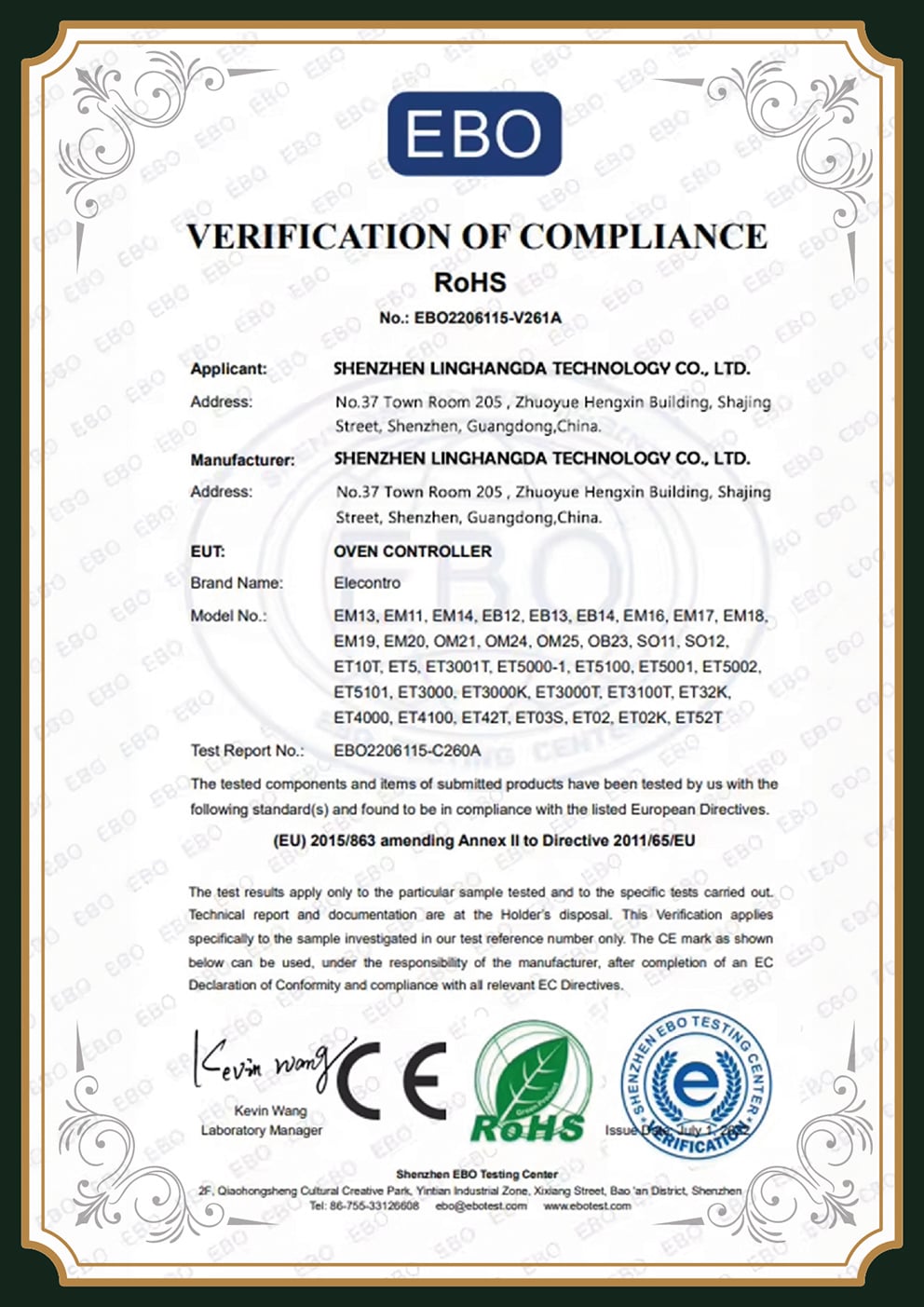
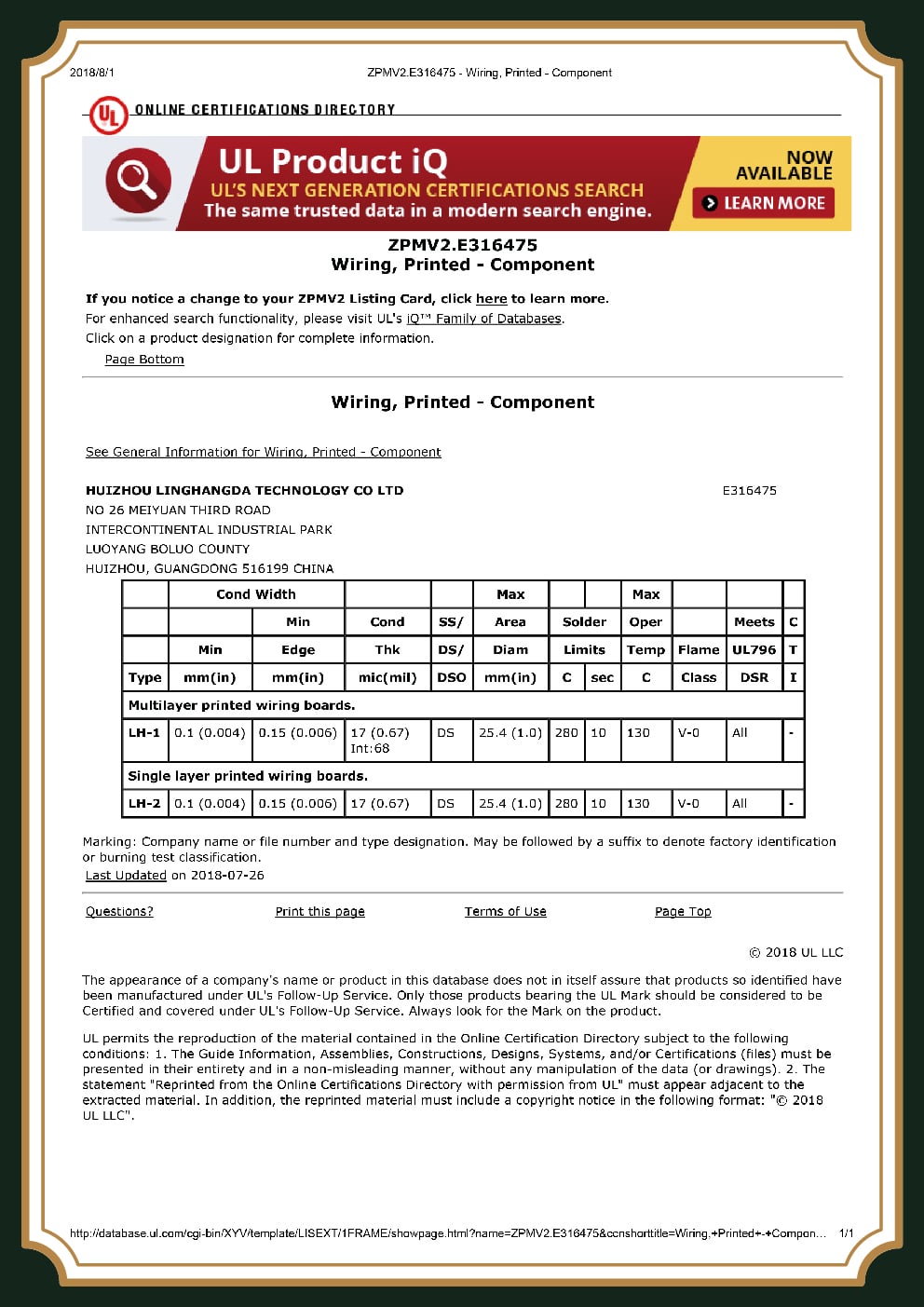
Certifications & Reliability Standards




Collaborative Partnerships
Client Engagements




Ordering Any-Layer HDI: Stackup Selection, Lead Time & DFM
No single price exists for an any-layer board: this price depends on your unique choices about your stack-up configuration. In order to provide the information relevant for you to begin accurately cost estimations, please view below the factors influencing the cost of any-layer.
Lamination cycles
The biggest single driver. Each sequential cycle repeats press, drill, plate, and image. Fewer cycles, lower cost — we size this to your routing, not to a catalog.
Layer count & structure
Any-layer vs 2+N+2 vs 3+N+3 changes both material and process. Whichever lowest structure still routes your board is the cheapest one to build.
Microvia geometry & fill
Copper fill, via-in-pad planarization, and tighter aspect ratios add process steps that affect price and yield.
Material & copper weight
Low-loss or high-Tg laminates and heavier copper shift both cost and the achievable line/space.
Reliability class & compliance
IPC-6012 Class 3, added testing, and IATF 16949 traceability raise inspection effort — and are non-negotiable where they apply.
Volume & schedule
Prototype and quick-turn builds carry different economics than production volume. Tell us the run and the date.
INTERACTIVE ENGINEERING TOOLKIT
Any-Layer HDI Tool Suite
Access our proprietary calculators to configure stack-ups, verify IPC-2226 compliance, estimate cost indexing, and build precise RFQ specifications for manufacturing.
TOOL // 01
HDI Structure Selector
Evaluate BGA pitch, I/O density, and board area constraints to determine the lowest-cost routing architecture.
TOOL // 02
Microvia Aspect Ratio Checker
Verify your microvia dimensions and dielectric depth against the IPC-2226 reliable plating window.
TOOL // 03
Cost & Size Estimator
Compare the footprint miniaturization percentage against the fabrication cost premium for various HDI tiers.
TOOL // 04
HDI RFQ Spec Builder
Generate a standardized, DFM-ready quotation block to ensure rapid and accurate manufacturing pricing.
Technical Resources
Any-Layer HDI PCB FAQ
What is an any-layer HDI PCB, and how is it different from standard 1+N+1 HDI?
An any-layer HDI PCB makes every layer an interconnect layer using copper-filled stacked microvias, so a trace on any layer can reach any other layer. Standard 1+N+1 HDI only adds microvia build-up on the two outer layers over a through-hole core. Any-layer removes that routing ceiling, which is why it is used when a dense BGA cannot fan out on 1+N+1 or 2+N+2.
Why does any-layer HDI cost more than conventional HDI?
Cost tracks the number of sequential lamination cycles. Each added cycle means another press, drill, plate, and image pass, so an any-layer stack costs more than a single-build board. Industry data puts a 6-layer HDI roughly 30-50% above a 4-layer board. The trade is real: a smaller board, fewer layers for the same routing, and higher assembly yield often offset part of the premium. We size the cycle count to your design so you are not paying for build-up you do not need.
Are stacked microvias reliable under thermal cycling?
Stacked microvias can fail by Z-axis separation at the target pad during reflow and thermal cycling, a risk IPC has flagged for high-reliability products. We manage it with copper-filled vias, controlled cycle counts, staggered transitions where the stack-up allows, and via protection per IPC-4761. Boards for aerospace and medical are built and inspected to IPC-6012 Class 3.
Can a China-based manufacturer build reliable high-end any-layer HDI?
Yes. Advanced any-layer stacks such as 3+N+3 are produced and field-proven by capable fabricators, and buyers report meeting both quality and reliability targets. The thing to qualify is not the country but the capability: ask for the achievable structures, the microvia fill and aspect-ratio limits, the IPC class, and a sample traceability report. In practice the real risk is not geography but an unproven process — a fabricator that cannot show its microvia fill data or its inspection records is the one to walk away from, wherever it happens to sit. Ask to see a coupon and a cross-section before you commit to volume, and qualify the line the same way you would qualify any high-reliability supplier. PCBark builds to IPC-6012 Class 3 and IPC-6016 and supports full DFM review before tooling.
How many layers can an any-layer HDI board have?
Any-layer construction scales with layer count because every dielectric layer carries its own microvia. Mobile and high-I/O designs commonly run 8 to 16 layers, and higher counts are produced for specialized applications. The practical limit on your design is set by stack-up symmetry, impedance targets, and the lamination cycle budget, which we confirm during DFM.
Do I actually need any-layer, or will 2+N+2 work?
When your most dense BGA fan out passes 1+N+1 or 2+N+2 within the layer limits that build type is cheaper, and we will inform you.Any-layer structure only provides a price advantage over multi-layer structures as via capacity is exhausted, or a pile-up of close-spacing devices would restrict a tighter structure, or layout area is the limiting factor. Send us the stack-up and smallest pitch components, and we’ll tell you the best price on the structure needed torouteyour design.
What microvia and trace geometries does PCBark support for any-layer HDI?
Copper filled 100 micron microvias have a 0.75 to 1 ratio for the line spacing to via opening, following the IPC-2226 standard for space and trace down to about 75 micron on an advanced build, all depending upon material used, number of layers and copper foil thickness. We use an “All in One Design”(ADI) DFM review to establish achievable dimensions based on your particular stack-up and design constraints.
What do you need from me to quote an any-layer HDI board?
Send us gerber data or ODB++ files along with your layer stack-up which define any target impedences, the complete build of materials, your IPC compliance level (ex. Class 3), the quantities you need, and the dates you would like to have your finished parts. Then, using our integrated DFM tools, we will review the structure you designed for a cycle count estimate, build material assessment and then provide a quotation and lead time for your application.
Start Your Build
Get an Any-Layer HDI PCB Quote from PCBark
Submit your structure and we will respond with the least costly structure designed to accommodate your HDI routing, the result of an all-encompassing DFM, and a quotation reflecting your specified IPC class. Over 16 years of EMS experience to support your project.
Request a Quote
Secure DFM Submission

![16-24 Layer PCB: Stackup, Lamination & Design Guide [2026]](https://pcbark.com/wp-content/uploads/2026/07/16-24-layer-pcb-guide-featured-2-150x150.png)


