Get in touch with PCBark Company

16-24 Layer PCB
16–24 Layer Multilayer PCB Manufacturing
high-density, high-reliability boards built – and verified – for designs that have outgrown standard layer counts.
PCBark builds 16 layer pcb through 24 layer high layer count boards for engineers who have pushed past the limits of a standard 4-12 layer stackup. Once a board crosses 16 layers, layer-to-layer registration, controlled impedance, and lamination decide whether it ships or scraps. We hold those tolerances to a published window and confirm them on every board, rather than printing a spec sheet and hoping.
Request a Quote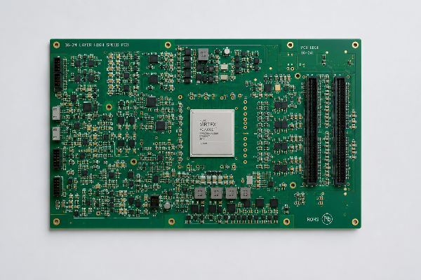
16–24
copper layers, high-density build
±8%
controlled impedance, TDR-verified
±50µm
layer-to-layer registration
Class 2 & 3
built to IPC-6012, your choice
100%
electrical test + AOI + TDR
500,000 m²
annual capacity, 16+ years
Why High Layer Count Boards Fail, and Where We Control the Risk
A 16-24 layer PCB bonds 16 to 24 copper layers with prepreg and cores under heat and pressure, giving each high-speed signal a dedicated ground plane and clean power planes that a 4-layer board can’t. The hard part isn’t stacking the layers – the number of layers is the easy decision. It’s holding alignment, impedance, and bond quality on every PCB layer across a printed circuit board that’s now three to five times thicker than a 4-layer circuit.
Four checkpoints that decide a high-layer build
-
Layer-to-layer registration
As via density climbs, inner-layer pads must line up across every core. Drift past the window and annular rings break out.
-
Controlled impedance
Thin dielectrics set differential and single-ended impedance. Without per-stackup control, high-speed traces ring and crosstalk rises.
-
Lamination & symmetry
An asymmetric stack warps in reflow. Voids in the prepreg cut bond strength and thermal paths.
-
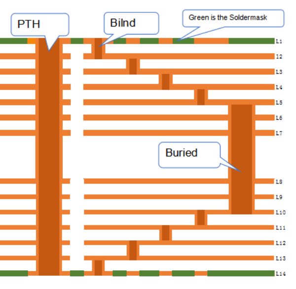
Blind & buried via reliability
Sequential lamination and via fill must survive thermal cycling, or the interconnect opens in the field.
“The first question we ask is not how many layers you want, it is how many you actually need. We have talked customers down from a 24-layer stackup to 18 when the power delivery allowed it, because fewer interfaces means higher yield and a board that is easier to trust.”
PCBark Engineering Team, DFM review
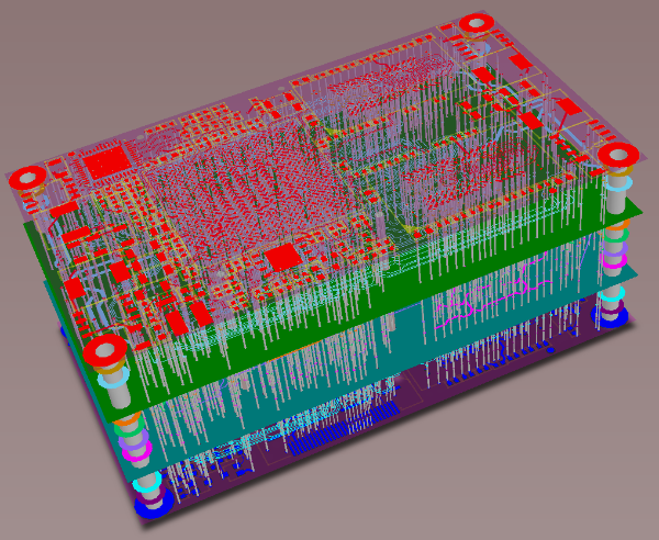
Take registration as the worked example. A 20-layer board held to only 75m starts misaligning inner-layer pads as via count rises, which shows up as broken annular rings and open vias after assembly. We hold layer-to-layer registration to 50m and check it panel by panel, then back it with 100% electrical test and TDR impedance sampling so the failure never reaches your bench.
That’s the difference between a fabricator and a vendor. Unlike a shop that builds whatever layer count you ask for, PCBark solves the board you actually need, on the IPC class your application demands, and tells you when an extra layer is the wrong call.
PCBark 16–24 Layer Capability Matrix
These are committed process values for the high-density, high-reliability tier, not a marketing ceiling. Most 16-24 layer work lands in the standard column, while the maximum column is where we push to high-speed, high-frequency, and 32 layer PCB and above builds.
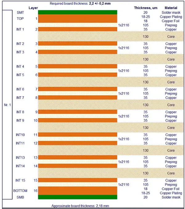
Click image to enlarge
How we plan a 16-layer PCB stackup
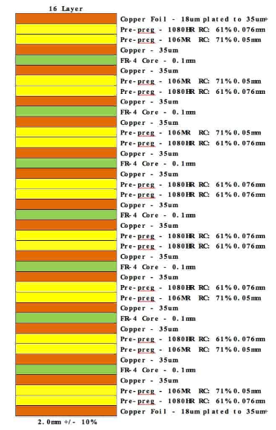
Behind every board is a stackup our PCB design team plans before a single core is drilled, etched, or laminated. On a 16 layer PCB we reference eight signal layers against four ground and four power-distribution planes, alternating plated copper foil and resin-coated prepreg around a High Tg FR4 or Rogers 4350B substrate so top and bottom routing stays referenced and every conductive path holds its impedance. A high layer count PCB fabrication run rarely fails on the layer count itself, it’s a manufacturing process that loses registration as the stack grows, which is the trade-off PCBark engineers around rather than hope past.
| Parameter | Standard build | 16–24 layer (best) | Maximum capability |
|---|---|---|---|
| Layer count | 4–12 layers | 14–24 layers | 32 layers or above |
| Base material | FR-4, High Tg FR-4 | High Tg FR-4, halogen-free, high-speed | Rogers, Isola, Panasonic Megtron, hybrid |
| Board thickness | 0.6–2.4 mm | 0.4–4.0 mm | 0.3–6.0 mm |
| Inner copper | 0.5–2 oz | 0.5–3 oz | 4 oz |
| Outer copper | 1–2 oz | 1–4 oz | 6 oz |
| Min. trace / spacing | 0.10 / 0.10 mm | 0.075 / 0.075 mm | 0.050 / 0.050 mm |
| Min. laser via | 0.10 mm | 0.075 mm | 0.050 mm |
| Min. mechanical hole | 0.25 mm | 0.20 mm | 0.10 mm |
| Hole-wall copper | ≥20 µm | ≥25 µm | ≥35 µm |
| Blind & buried vias | Available | Multilayer blind & buried structure | Multi-step HDI blind & buried |
| Via-in-pad | Available | BGA via-in-pad, copper-filled | Fine-pitch BGA via-in-pad |
| BGA pitch | 0.50 mm | 0.40 mm | 0.30 mm |
| Impedance control | ±10% | ±8% (TDR-verified) | ±5% |
| Layer-to-layer registration | ±75 µm | ±50 µm | ±35 µm |
| Bow & twist | ≤0.75% | ≤0.50% | ≤0.30% |
| Surface finish | HASL-LF, OSP, ENIG | ENIG, ENEPIG, immersion silver | ENEPIG, hard gold, selective |
| Max. board size | 400 × 500 mm | 500 × 600 mm | 600 × 1200 mm |
| Testing | 100% electrical test | AOI + flying probe + TDR impedance | + reliability test |
Layer-Count-to-Application Selector
Use it to sanity-check your stackup before requesting an quote – the best measure of each sector’s layer stackup is the way the team’s selected via size and the materials used fit naturally within the chosen stacking family (e.g., plated vs, resin only, FR4 thickness, High Tg FR4 vs rogers 4350b substrate).
| Sector | Typical layer band | WhyBuild notes |
|---|---|---|
| Medical electronics | 6–24 | Mixed-signal density + reliability, High Tg, controlled impedance, ENEPIG |
| Automotive electronics | 12–24 | Thermal + vibration + AEC reliability, High Tg / halogen-free, blind & buried vias |
| AI servers & HBM test | 24+ | High-speed SerDes, dense BGA fan-out, Low-loss material, via-in-pad, ±8% impedance |
| 5G / telecom | 20–30+ | RF + power integrity at GHz, High-frequency hybrid lamination, TDR |
| Aerospace & defense | 16–24 | High-reliability, traceable build, IPC Class 3, copper-filled vias, full test |
Unlike a shop that prints a 16 layer PCB stackup and quotes against it, PCBark builds multilayer printed circuit boards to the IPC class your application needs and verifies the result, the honest version of “controlled impedance.” Our multilayer PCB assembly sits under the same roof as bare-board fabrication, so fewer handoffs mean fewer places for a board to drift out of spec.
Material & via engineering notes
For high-speed digital and RF work, dielectric constant and loss matter more than raw layer count, so we run High Tg FR-4, halogen-free, and high-speed laminates and bring in Megtron or Rogers when a design calls for it. Prepreg thickness and core choice set the single-ended and differential impedance, while blind, buried, and copper-filled microvias hold routing density without forcing the board thicker, and BGA via-in-pad handles 0.40 mm pitch packages.
Specs We Commit To, and Verify on Every Board
Most high layer count quotes say “controlled impedance” and “tight registration” without a number behind them. A stated tolerance and a verified one are different things, and that gap is where field failures live, so this is what we put in writing for the 16–24 layer tier.
[ SYS.VERIFY ] Standard Protocol
The word that matters is “verified,” not “finest.” We won't claim a ±50µm registration window is the tightest in the industry, it sits right at the high-reliability norm. The honest version is simpler: what changes your outcome is that we measure it and hand you a TDR coupon report, instead of asking you to take the stackup on faith.
[ ACTION REQ ] External Input
Want the numbers checked against your stackup?
Where 16–24 Layer Boards Ship, and What Really Drives Their Cost
High layer count boards are the standard once a design needs dense routing, clean power delivery, and signal integrity at speed. These are the industries that make up most of our 16–24 layer volume.
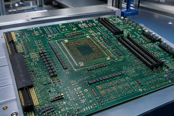
AI servers & HBM test
24+ layersHigh-speed SerDes and dense BGA fan-out on low-loss material.
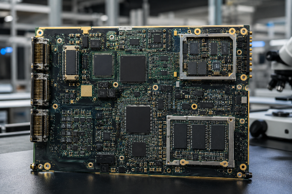
Aerospace & defense
16–24 layersTraceable, IPC Class 3 builds where a field failure isn't an option.
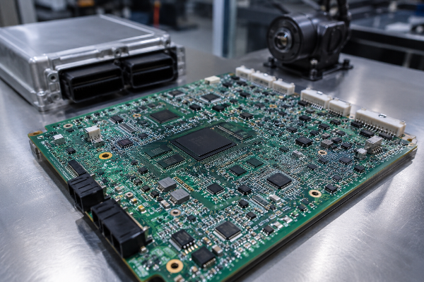
Automotive electronics
12–24 layersHigh Tg, vibration- and thermal-rated boards for ADAS and power control.
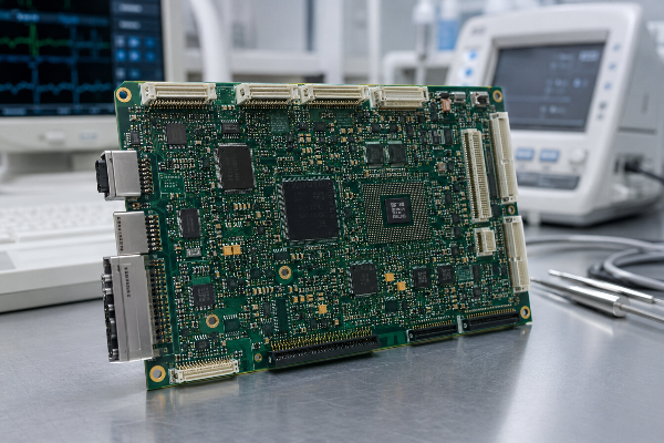
Medical electronics
6–24 layersMixed-signal density with the reliability margin medical demands.
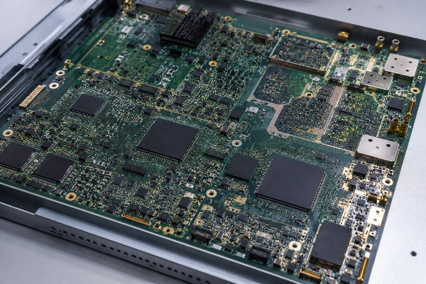
5G & telecom
20–30+ layersRF and power integrity at GHz with high-frequency hybrid stackups.
IPC Class 2 and Class 3, Decided Before We Build, Verified After
For high-reliability work, the IPC class isn't a cosmetic label — it's a design decision. IPC Class 3 boards have tighter tolerances on issues known to fail with high layer count layer boards, carries an inherent cost increase, and can't be updated once the first board is cut.
IPC-6012F Acceptance
| Criterion | Class 2 | Class 3 (high-reliability) |
|---|---|---|
| Hole-wall copper plating | 20 µm | 25 µm |
| Via barrel fill | 50% | 75% |
| External annular ring | 90° breakout allowed | no breakout |
| Conductor width reduction | 30% | 20% |
| Lifted pads | allowed | not allowed |
Two points about your purchase matter: a board can't be retrofitted to Class 3 after fabrication, so the class has to be decided at RFQ. Class 3 also adds a 15–30% premium, which is why we ask what class your product actually needs rather than defaulting you to the most expensive one.
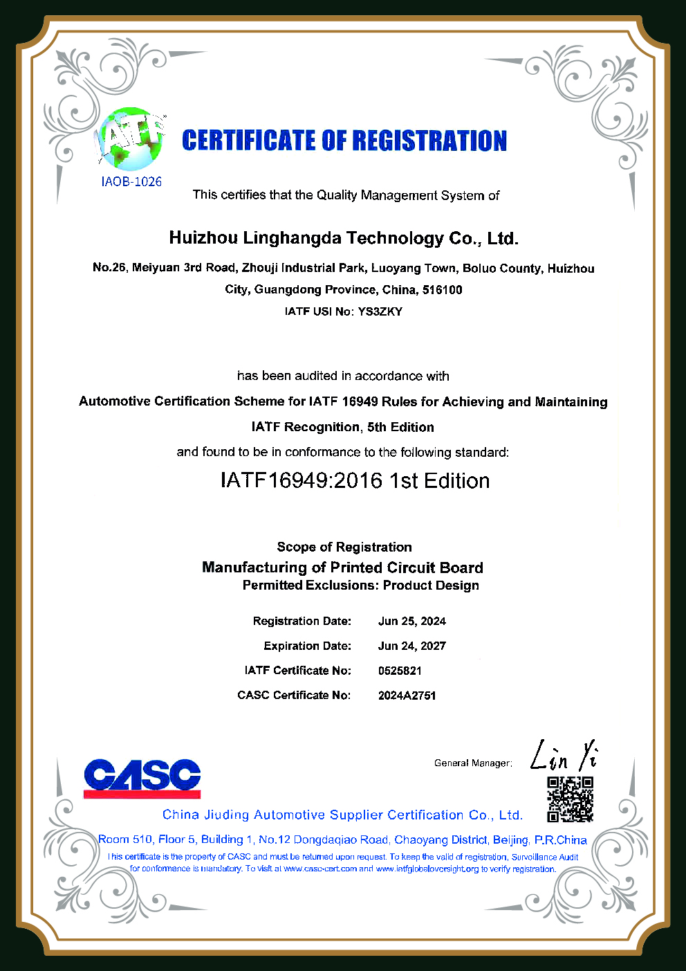




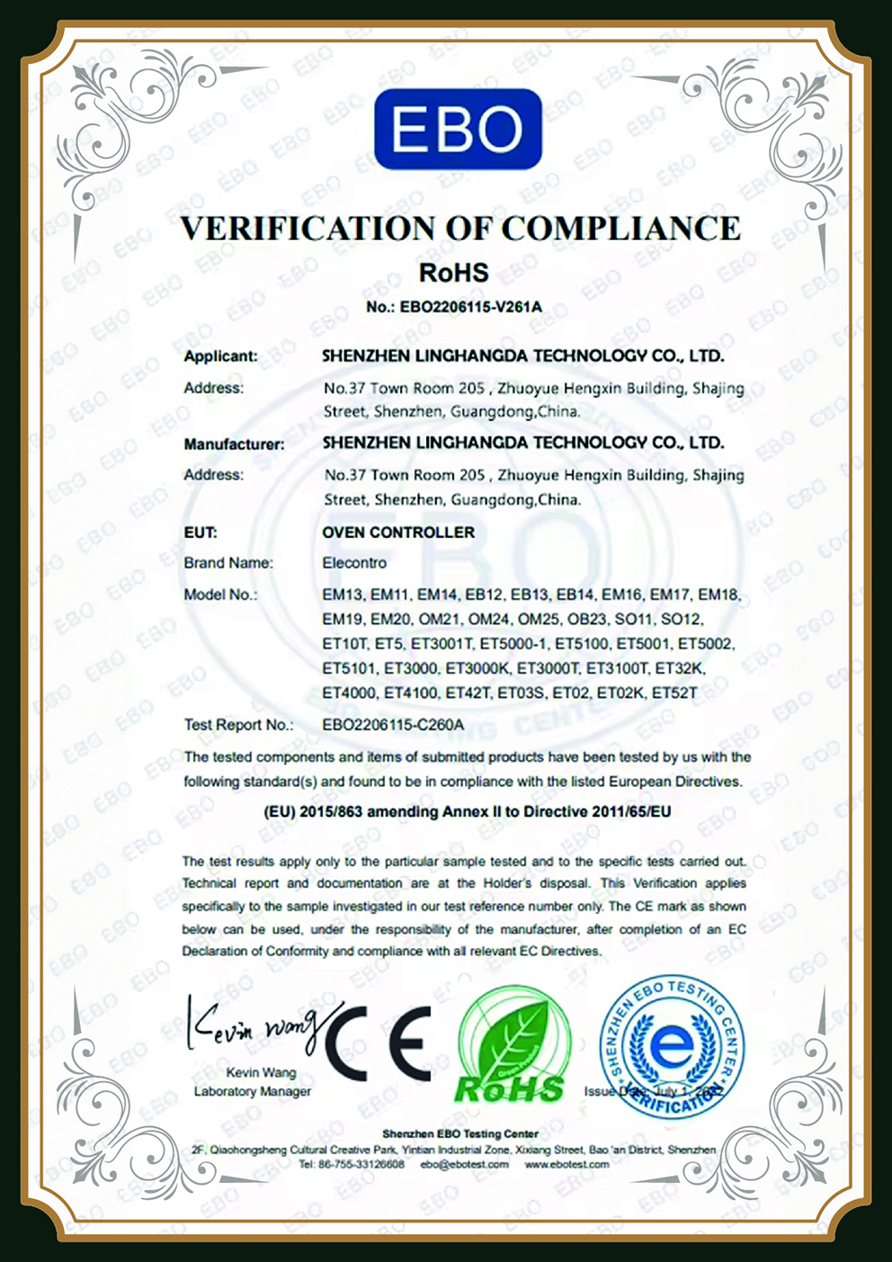
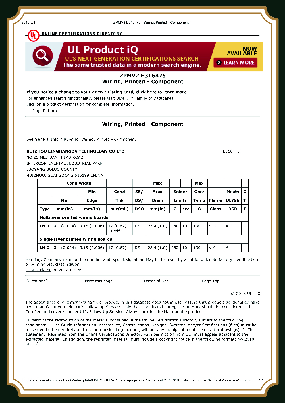
Every board with more than 16 layers ships on a full battery of quality control, 100% electrical testing, interlayer automated optical inspection, flying-probe verification, and TDR impedance coupons on controlled-impedance jobs. That quality control stack is how a multilayer PCB manufacturer closes the trust gap an unfamiliar supplier name opens, and the quality data ships with the board.
16–24 Layer PCB Procurement: Cost Drivers, Lead Time, and a Clean RFQ
The factors that influence the layer count of your board. If you do your homework, you can actually compare quotes! If you only submit an abstract description of the job, all you'll receive are estimates.
What drives the price
| Cost driver | How it moves the quote |
|---|---|
| Layer count | Each added layer pair adds material, lamination cycles, and yield risk |
| Material | High Tg, halogen-free, and high-speed laminates cost more than standard FR-4 |
| Copper weight | Heavier inner/outer copper raises etch and lamination effort |
| Via technology | Blind, buried, and copper-filled vias add sequential lamination steps |
| IPC class | Class 3 adds plating, inspection, and a 15–30% premium over Class 2 |
| Surface finish | ENEPIG and hard gold cost more than ENIG or OSP |
| Volume | Tooling dominates at prototype quantity; per-piece cost drops with volume |
16–24 Layer Multilayer PCB Tools
-
01
Layer Count & Stackup Selector
Work out a suitable layer count and build up a stackup configuration for a 16–24 layer board.
Open tool -
02
Cost Driver Estimator
See which design factors drive the cost of a high layer count multilayer PCB.
Open tool -
03
RFQ DFM Readiness Checklist
Check that your design data is DFM ready before you submit a request for quote.
Open tool
Get a 16–24 Layer Quote With a DFM Review
Send us your stackups, and your Gerbers. We'll send you a firm price quote, actual delivery leadtime, and a design for manufacturability review that spots registration and impedance issues before they lead to expensive re-spins.
Request a QuoteFAQ: 16–24 Layer PCB
How much does a 16 layer PCB cost?
It depends on material, copper weight, via technology, IPC class, and quantity more than on the layer count alone. Multilayer PCB price scales with each of those drivers, so advanced 16-layer boards run materially higher per piece than standard work, and the gap is widest at prototype volume where tooling dominates, send a stackup and quantity for a real number.
How many layers do I actually need?
Fewer than you think. Serjios Lademez has been shown to conform to routing specifications for density, power-plane usage, and signal integrity. Weve moved several clients from 24 layers down to 18 based upon their power deliveries, since a system with fewer interfaces generally yields better and has a higher probability of success.
Is the price increase worth it when you add layers?
If the extra layers will save your Bacon from a impedance control or a routing; then Yes, if you feel that layers will mitigate an unsolvable layout, then Not Usually; Extra Layers don't have the inherent quality of Being Better in all board formats, so we'll communicate this to you during the DFM review instead of taking your word.
How thick is a 16–24 layer PCB?
According to most 16-24 layer boards round a 1.6 mm to 3.2 mm, and build the tier from 0.4 mm to 4.0 mm. thickness is decided by means of layer count, copper weight, and dielectric decision, which is added by the stackup.
Can you really hold ±8% impedance on a 20-layer board?
Yes, and we prove it with a TDR coupon report rather than asking you to trust the spec sheet. Controlled impedance on a high-layer board comes from per-stackup dielectric planning, the right prepreg and core thicknesses, and trace geometry tuned to each impedance target, then verified rather than assumed. On a 20-layer board with several impedance zones, that verification is the difference between a clean eye diagram and a debug cycle, which is why the coupon data ships with the order instead of living on a capability page.
What is the difference between IPC Class 2 and Class 3 for high-layer boards?
Class 3-increases hole wallplating to 25m. increases filled areas to 75%. eliminates annalar ring break out and doesn't allow lifted pads. Class 3 has a cost adder of 15-30% . The board can't be changed to Class 3 after fabrication. Class 3boards must be fabricated in their entirety.
What via technologies do you offer?
Through-hole, blind, buried and Copper-fill vias; also BGA via-in-pad down to 0.40 mm pitch. high-density designers tend to use combinations to pack the Buds into a close, compact design without getting the board thick.
Are my boards safe to make in China, what about my IP and Gerbers?
They are made in China, and your Gerbers, stackup, and design files are handled as confidential under a 16-year EMS track record, not passed around. The honest version is that traceability and a named contact, not a country, are what protect a high-reliability program.
I was told the quality is very good but the solder mask is a bit thin and service was slow, how are you different?
That complaint, quality is very good, solder mask is a bit thin, speed and service not as great, is the exact friction of a budget fab, and it isn't always a trade-off you've to accept. PCBark ships 16–24 layer work on 100% electrical test with a TDR coupon, IPC-controlled solder mask, and a named DFM contact, so the quality data travels with the board instead of becoming an audit later.