Get in touch with PCBark Company

6-Layer PCB
6-Layer PCB Fabrication & Assembly, Stackup, Specs & Manufacturing
Production-grade 6-layer boards with published impedance tolerance, full inner-layer traceability, and turnkey assembly under one roof, built to IPC-6012 Class 2 and Class 3.
- 6-Layer PCB
- IATF 16949
- IPC Class 2 & 3
- 16+ Years
- 500,000 m²/yr Capacity
- No MOQ
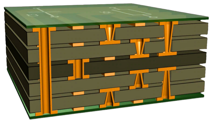
Specifications
- 1–40+ Layer count (6L core config)
- 0.20–6.0 mm Board thickness (1.6 mm std)
- 3 mil Min trace / space
- 0.15 mm Min mechanical via (6 mil)
- ±10% / ±5% Impedance tolerance
- ENIG·HASL·OSP Surface finishes
- 48–72 h Prototype lead time
- None Minimum order quantity
From 4-Layer Bottlenecks to a Production-Ready 6-Layer Board
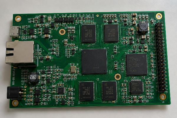
A 6 layer PCB stacks four signal layers around two dedicated power and ground planes, giving high-speed traces an uninterrupted reference plane that a 4-layer board can’t. That single change cut electromagnetic interference (EMI), tightens controlled impedance, and frees routing channels for dense BGA and FPGA fanout.
You reach for six layers when a 4-layer design runs out of room: split planes, crosstalk between adjacent signal layers, or no clean return path under a 100 MHz+ bus. The cause is physical, two layers can’t carry both solid references and the signal density a modern processor need.
More layers aren’t automatically better, though. A widely repeated engineering caution puts it plainly: adding layers “isn’t always the case” for a better board, and the right count is the one that give every critical net a reference plane at the lowest stable cost. PCBark treats 6-layer as a fit-for-purpose step, validated against build standards such as NASA-STD-8739.3 workmanship for electronic hardware.
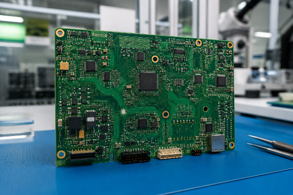
4 → 6 → 8 Layer Graduation Map
| Trigger in your design | 4-layer | 6-layer | 8-layer |
|---|---|---|---|
| Single split-free power rail | Adequate | Headroom | Over-built |
| 2–3 voltage rails + 1 high-speed bus | Plane conflict | Right fit | Headroom |
| Controlled impedance + EMI margin | Marginal | Solid (2 GND refs) | Solid |
| Dense BGA (≥0.5 mm pitch) escape | Microvia-limited | HDI-capable | Best routing |
| RF front-end + analog/digital isolation | Hard | Achievable | Achievable |
6-Layer PCB Stackup Configurations & Controlled Impedance
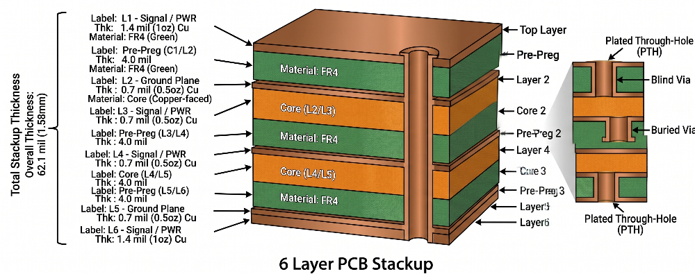
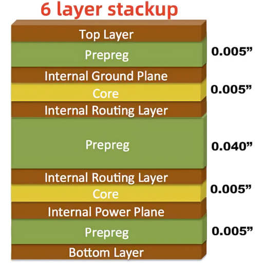
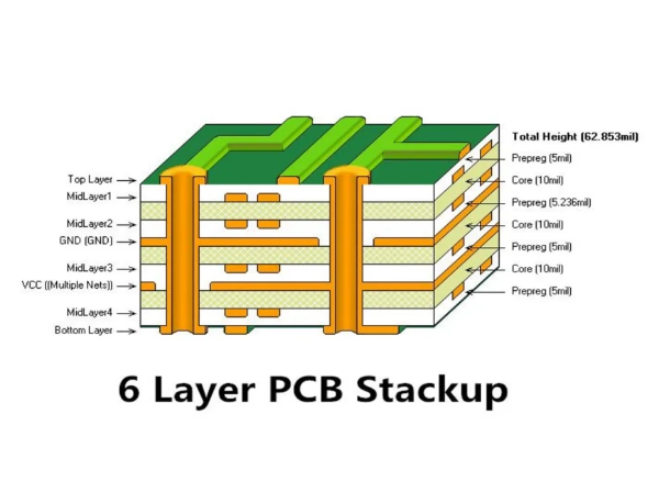
Two configurations cover most 6-layer work. The standard SIG / GND / SIG / PWR / GND / SIG arrangement sandwiches routing between solid planes for the best EMI control; a routing-dense SIG / GND / SIG / SIG / GND / SIG variant trades one reference for two adjacent inner signal layers.
Stackup is where a 6-layer board earns its cost. Signal pain here is real, route a 90 Ω differential pair over a split plane and you get reflections, timing skew, and failed compliance. Its cause is an interrupted return path, so the fix is a symmetric stackup that keeps every high-speed trace tightly coupled to a solid copper reference.
| PRIORITY | RECOMMENDED 6-LAYER STACKUP | REFERENCE / IMPEDANCE | TYPICAL USE |
|---|---|---|---|
| Best signal integrity / EMI | SIG / GND / SIG / PWR / GND / SIG | L1&L6 microstrip, L3 stripline — 50 Ω / 100 Ω | High-speed digital, ADAS, BMS |
| Max routing density | SIG / GND / SIG / SIG / GND / SIG | 2 inner routing layers, thick core split | Dense BGA breakout |
| RF / mixed-signal isolation | SIG / GND / PWR / GND / SIG / GND | Dedicated GND moat under RF | 5G front-end, sensors |
| Tight Z-axis (wearable) | Symmetric 1.0 mm build | Thin prepreg, ±5% impedance | Medical wearable HDI |
Engineering Note, Impedance you can verify
Engineering Note, Impedance you can verify
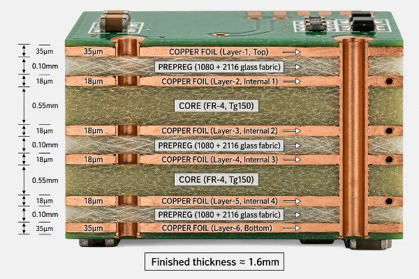
PCBark builds to a published ±10% impedance tolerance as standard and ±5% on request, and ships a TDR (time-domain reflectometry) report against your target on controlled-impedance orders. Symmetry matters: a center core flanked by matched prepreg and copper foils prevents the warp that asymmetric 6-layer stacks suffer during lamination.
Standard finished thickness is 1.6 mm (62 mil), with 0.8, 1.0, 1.2 and 2.0 mm builds for space-constrained or backplane work, the same 6-layer pcb thickness range engineers expect, held to ±10%. Differential de-embedding follows methods in IEEE 370, and dual-polarized mm-wave structures on HTML six layers are now documented in published filings such as WO 2023/165634 A1.
Engineering Note, 6-Layer Stackup Design Rules
Engineering Note, 6-Layer Stackup Design Rules
On a six-layer pcb stack-up, the dielectric thickness between each signal layer and its reference plane set the trace width you need for a target impedance. Keep the prepreg between L1 and the L2 ground plane thin so a controlled-impedance high-speed signal stays tightly coupled, and run Layer 3 as stripline between the inner ground plane and the power layer.
Capacitance between that power plane and ground layer adds natural decoupling, which lowers EMI and helps EMC compliance. Follow the symmetry design rule around the center core to hold impedance and prevent warp, and make sure every high-speed signal is routed without crossing a plane split. A standard 6 layer pcb stackup example builds to 1.6 mm, and we accept stackup and design-rule files exported from common PCB design tools, so your advanced PCB design imports cleanly into our 6-layer pcb design flow. Run design rule checks on the signal and power nets in your PCB layout before release: pairing the power plane with the ground plane keeps every signal return path continuous, holding signal integrity without compromising EMI margin.
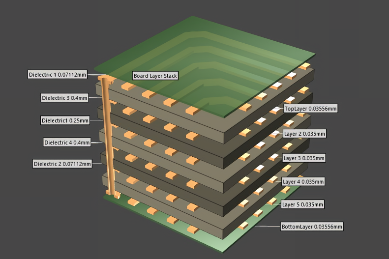
• HOVER COMPONENT TO ALIGN •
Production-Grade vs Commodity Prototype Fabs, Where the Difference Shows
Honest framing: this isn’t “we’re cheaper.” A $2, 48-hour proto and a traceable production supply are two different jobs, and that headline price applies only to boards under 50 × 50 mm. Pain shows up later: an unverified inner layer or an impedance figure no one will commit to in writing.
Lifecycle math follows the field consensus that the cheapest board upfront is rarely the lowest-cost decision. A six-layer redesign forced by a bricked inner layer, or an 8-layer respin caused by poor impedance control, costs far more than the per-board delta, a trade-off explored in signal-integrity literature indexed by IEEE Xplore.
+30–40%
Typical board-cost step from 4-layer to 6-layer — the point at which design correctness and impedance proof, not unit price, drive total cost.
Source: Sierra Circuits PCB price composition.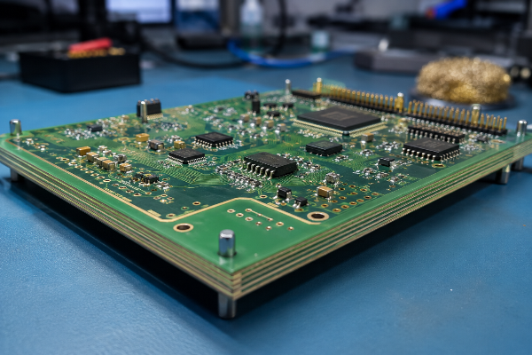
Decision Factors Specification Matrix
| [Decision Factor] | Commodity Prototype Fab | PCBark Production EMS |
|---|---|---|
| Impedance commitment | “Yes” with no published ± | ±10% / ±5% + TDR report |
| Inner-layer proof | Pass/fail e-test only | 100% e-test + micro-section + X-ray |
| Automotive credential | Not shown | IATF 16949 + IPC-6012FA |
| Assembly | Bare board, or separate | Turnkey SMT/BGA/THT + sourcing |
| Traceability | Lot-level | Serialized + ≥5-year data archive |
| Volume model | Proto pricing tiers | No MOQ + tiered mass-production |
Certifications & Inner-Layer Quality Assurance
Trust on a six-layer board is earned at the layers you can’t see. Here, a supplier who claims a cert but can’t produce evidence on audit is met with named standards and recorded test data, not adjectives.
- IATF 16949 Automotive QMS
- ISO 9001:2015 Quality system
- ISO 14001 Environmental
- UL Listed
- IPC Class 2/3 Workmanship
- RoHS / REACH Compliance
CONTINUOUS VERIFICATION FEED: AOI SCAN MODE
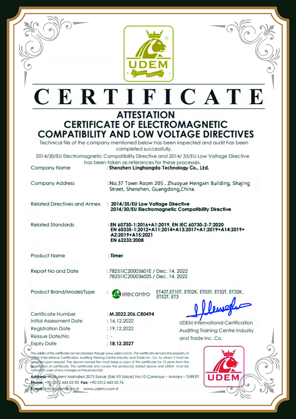
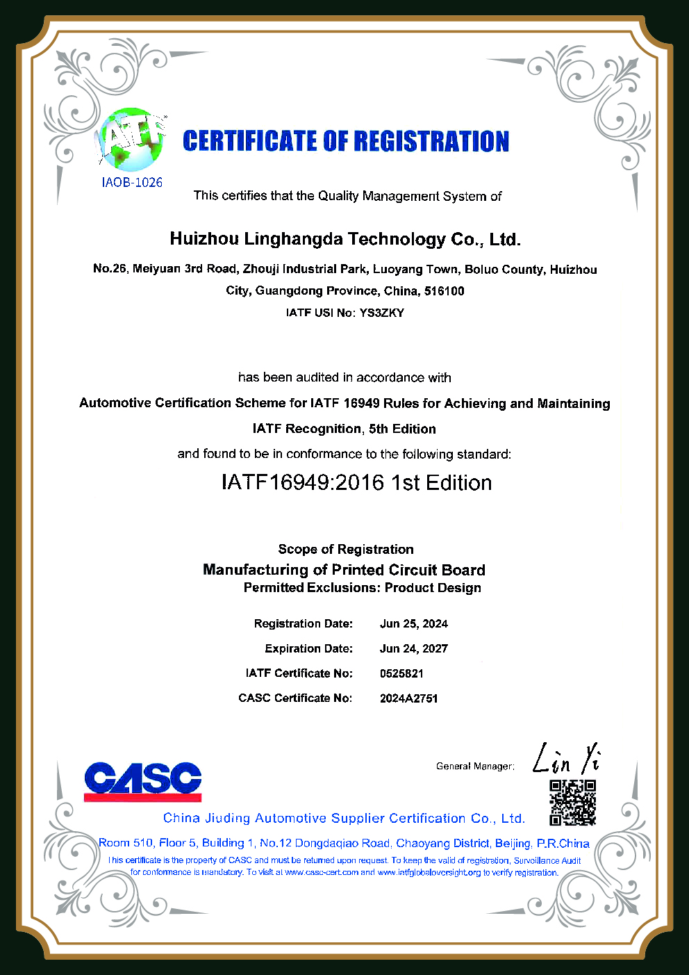




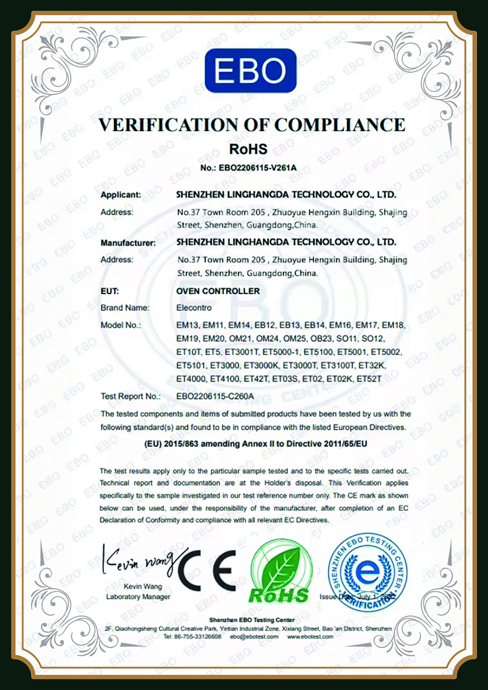
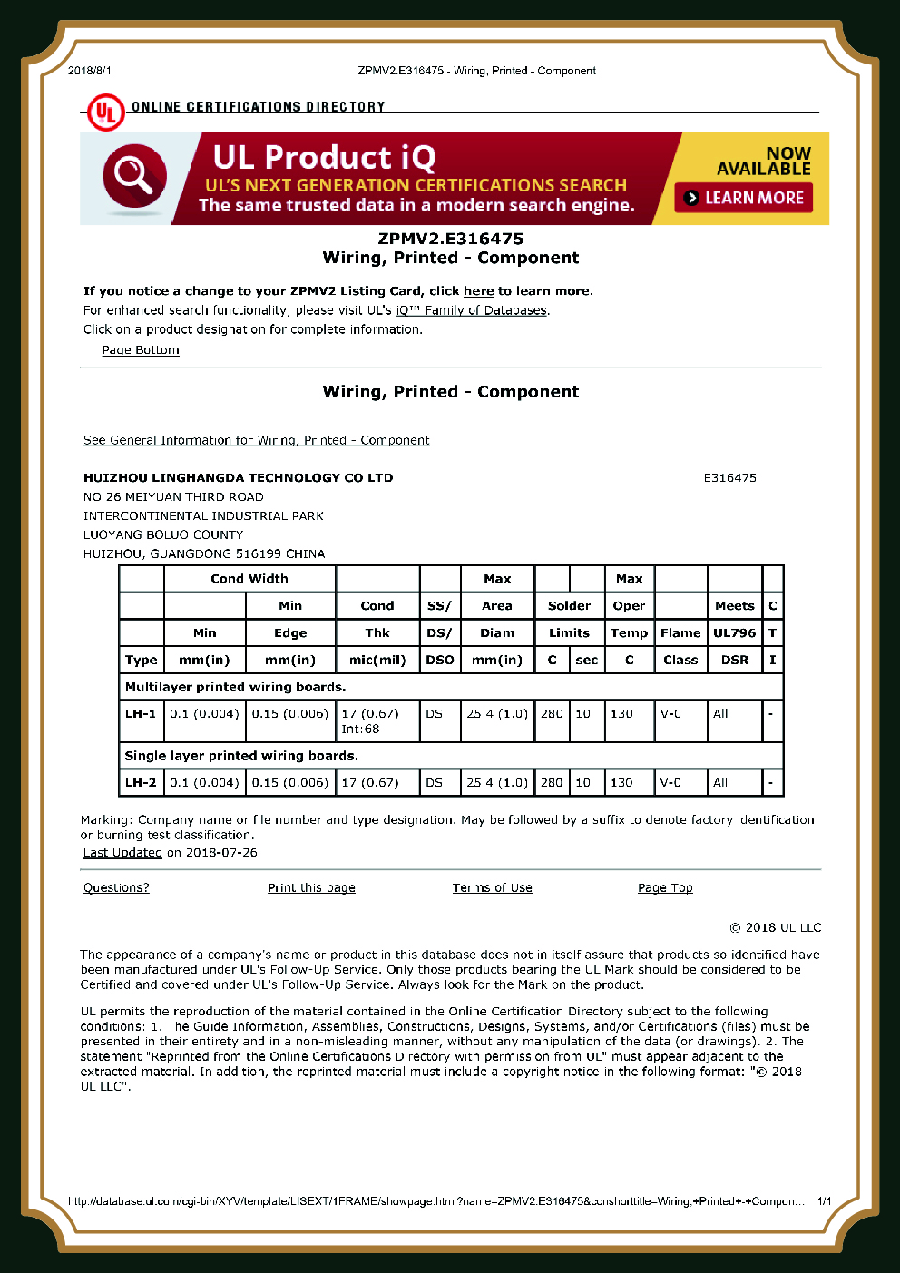
Every 6-layer order passes 100% electrical test, automated optical inspection on each inner core, X-ray on BGA joints, and cross-section analysis of copper thickness and plating. Acceptance follows ISO 14001-backed process control and IPC-A-600 visual criteria, with results archived per lot.
What you get instead is evidence you can hold: a cross-section image of your inner copper, the flying-probe net-list result, and the impedance TDR trace, archived against your lot number for at least five years. A commodity fab that ships only a pass/fail line can’t show you the inner layers; we record them, which is what turns “trust us” into proof.
Procurement Guide: 6-Layer Cost Drivers, Lead Time & Ordering
Buyer pain here is the bait quote — a low headline that changes once a “custom” stackup or a real size enters the picture. Instead of a single number, we publish the cost drivers, so you can predict where your 6 layer pcb cost moves before you order.
Behind a quote is real capacity, and that’s what protects your lead time. As a 6 layer pcb manufacturer running fabrication and turnkey assembly across 500,000 m²/yr with LDI imaging, in-line AOI, X-ray and flying-probe test, we keep a production order from stalling behind the prototype queue, the hidden cost commodity shops rarely mention. Our honest answer on cost is to name the trade-off up front, not bury it in a revised invoice.
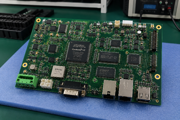
[CAM.1] 3:2 MACRO
6-Layer Cost-Driver Breakdown
Layer step: 4→6 layers adds roughly 30–40% board cost (Sierra Circuits)
Board size & panel utilization, the real driver behind “cheap” proto limits
Copper weight & controlled impedance (TDR adds test, not guesswork)
Base material, FR-4 vs high-Tg vs Rogers/PTFE for RF
Surface finish, ENIG and ENEPIG cost more than HASL/OSP
Volume, No MOQ for prototypes, tiered pricing into mass production
Prototype-to-Production Readiness Ladder
| Stage | Lead time | What you send |
|---|---|---|
| Prototype | 48–72 h | Gerber + stackup + impedance target |
| Small batch / bring-up | ~1 week | Gerber + BOM (for assembly) |
| Mass production | Tiered schedule | Forecast + approved first article |
Ordering in four steps
Upload your Gerber for a quote, receive a free DFM review, approve the first article, then move to production, all with one engineering contact. Need a number for your exact size and class?
Request a quoteand we’ll price your specific 6-layer build. Design-for-manufacturing guidance follows public references such as the NASA-STD-8739.4 workmanship set.
6-Layer PCB Engineering Tools
Stackup Selector
Configure optimal dielectric thickness, prepreg types, and impedance profiles for 6-layer manufacturing.
EXECUTE
Layer Recommender
Analyze signal routing density to determine ideal ground, power, and signal plane distributions.
EXECUTE
Cost Estimator
Calculate real-time production costs based on base materials, surface finishes, and volume requirements.
EXECUTE
DFM Checklist
Verify gerber files against 6-layer manufacturing constraints (trace/space, drill sizes) to prevent delays.
EXECUTE
01
How much more does a 6-layer PCB cost than a 4-layer board?
Stepping from four to six layers adds roughly 30–40% to board cost, according to Sierra Circuits’ price composition data. Those extra layers buy two solid reference planes and routing room, usually cheaper than the 8-layer respin a cramped 4-layer design forces later.
02
Is the $2 / 48-hour 6-layer price real?
That headline applies only to small prototypes under about 50 × 50 mm, a point experienced buyers raise often on forums. For a real size, controlled impedance, or assembly, request a quote on your actual Gerber so the price reflects your board, not a teaser.
03
Do you guarantee controlled impedance on 6-layer boards?
Yes, we build to ±10% impedance tolerance as standard and ±5% on request, and ship a TDR report against your target. Engineers on EEVblog note that some low-cost fabs say “impedance controlled” without publishing a tolerance; we publish ours.
04
Is there a minimum order quantity for 6-layer PCBs?
No — none at all. We run 6-layer prototypes with no MOQ, then tier pricing as you scale.
05
What is the standard 6-layer PCB stackup and thickness?
A common configuration is SIG/GND/SIG/PWR/GND/SIG at a 1.6 mm finished thickness. We also build 0.8, 1.0, 1.2 and 2.0 mm symmetric stacks for space-constrained or backplane designs.
06
When should I move from a 4-layer to a 6-layer board?
Move up when a 4-layer design can no longer give every high-speed net a solid reference plane, when you need two or more clean voltage rails, or when dense BGA escape and EMI margin run out of room.
07
Is an 8-layer PCB better than a 6-layer? (6 layer pcb vs 8)
Not by default, more layers aren’t always better. Stay at six layers when every high-speed net already has a solid reference plane and your rails fit two power/ground planes; step to eight only when routing density or added plane pairs demand it. We quote both so the layer count follows your design, not a habit.
08
How fast can I get a 6-layer prototype?
Our 6 layer pcb prototype lead time is 48–72 hours with no minimum order quantity. Send a Gerber and stackup with your impedance target, and a 6 layer pcb fabrication quote with a free DFM review comes back the same day.
09
What materials and finishes do you offer for 6-layer PCBs?
FR-4 Tg150/170, Rogers, PTFE, polyimide, ceramic and metal-core bases, with ENIG, HASL, OSP, immersion silver/tin, ENEPIG and gold fingers. We match the material to your impedance, thermal and frequency targets.