4-Layer PCB

4-Layer PCB Manufacturing, Custom Boards with Controlled Impedance

Manufacturer-direct 4-layer PCB fabrication built to IPC-6012 Class 2 and Class 3, with impedance verified by on-site TDR, not catalog math. Upload your Gerber and get an all-in quote in 24 hours.

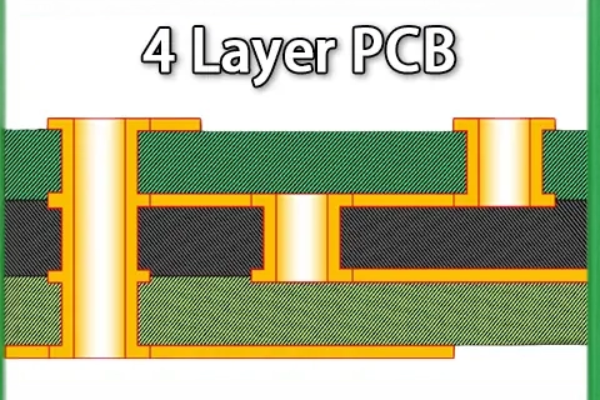
A 4-layer PCB is a printed circuit board with four copper layers, two outer signal layers and two inner planes for ground and power, laminated around an FR-4 core. Those inner reference planes are what give a 4 layer pcb its controlled impedance, lower EMI, and tighter routing density versus a 2-layer board. PCBark builds them in a single lamination cycle, in-house, from prototype to volume.

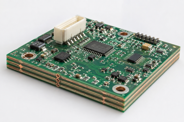
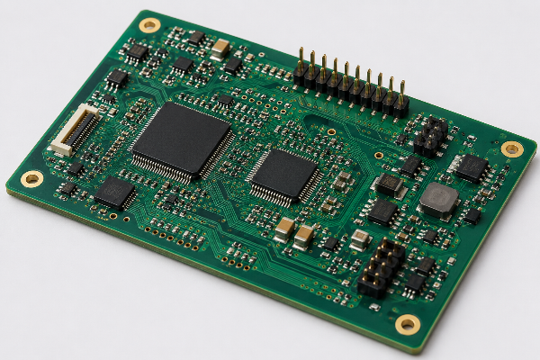
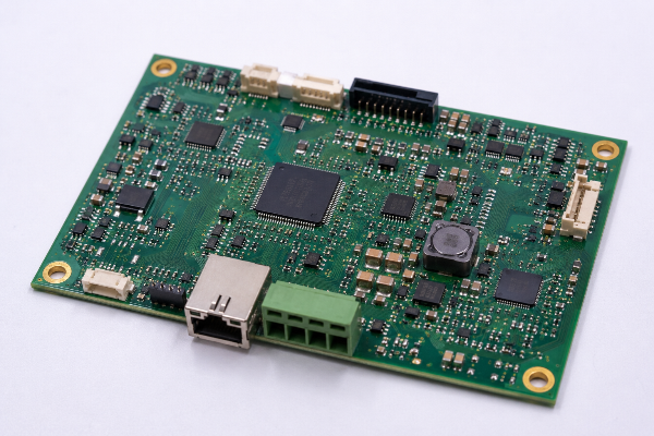
Green 4-layer PCB with connector and surface-mount components, board edge showing four laminated copper layers around an FR-4 core

4-Layer PCB Specifications

4Copper layers (IPC Type 3/4)
±10%Impedance tolerance (±5% on request)
0.3–6.0mmFinished thickness (std 1.6mm)
3 milMin trace / space (0.075mm)
Class 2/3IPC-6012F build capability
7Certifications (IATF16949/UL/ISO…)

Why Move to a 4-Layer PCB: Signal Integrity, EMI, and Routing Density

Move to a 4-layer board when you need controlled impedance, a quiet return path, dense fine-pitch routing, or lower EMI, the two inner planes solve problems a 2-layer board physically cannot.

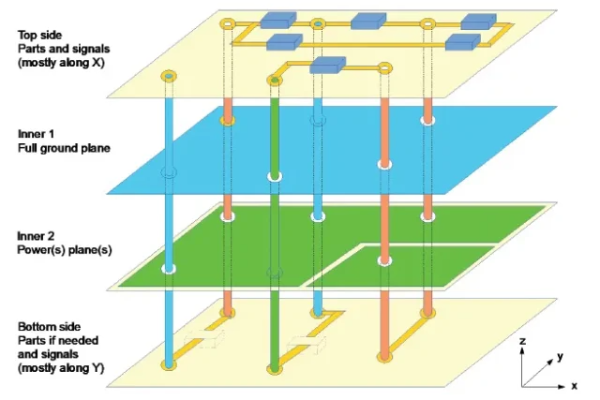
Unlike a 2-layer board, where high-speed return current wanders and raises the risk of crosstalk and radiated-emission problems above 100 MHz, a 4 layer pcb places a solid ground plane on layer 2. That continuous reference give every top-layer trace a low-inductance return path, the structural reason electromagnetic interference (EMI) and signal-integrity problems fall, with improved signal integrity, better thermal performance, and higher routing density than a 2-layer pcb. For any design with a controlled-impedance net or dense fine-pitch routing, moving to four layers is the right call.

4-Layer PCB Signal Integrity Layout
VIEW // FIG.01-LAYER-STACK

2-Layer vs 4-Layer vs 6-Layer, Comparison Matrix

Attribute
2-Layer
4-Layer
6-Layer
Dedicated reference planes
0
1–2 (GND + PWR)
2–3
Controlled impedance
Not practical
Yes, ±10%
Yes, ±10%
EMI / return-path quality
Weak
Strong
Strongest
Lamination cycles
1 (single)
1–2
Relative fabrication cost
2–5× (proto), ~2–3× (volume)
3–7×
Typical fab lead time
3–5 days
Quick-turn–10 days
10–15 days
Best for
Simple, low-density
High-speed, EMI, density
Dense diff-pairs, HDI
Request a custom 2-layer-vs-4-layer comparison for your board, we map the trade-off to your impedance and EMI targets. More layers are not automatically better. For most connected products, a 4-layer board already balances performance, EMC, and cost, engineers jump to 6 layers mainly when dense differential pairs need two reference planes [PROOF, contradicts “more layers = better”].

Where 4-Layer Boards Earn Their Keep

Automotive

ECUs and motor controllers facing thermal cycling and vibration (IPC-6012EA addendum).

Medical & IoT

Diagnostics, sensors, and connected devices where EMI control and reliability decide field life.

Industrial Control

Motor drives in noisy three-phase switching environments that must run for years.

High-Speed Digital

USB, HDMI, and PCIe interfaces that demand a defined impedance reference, where IEEE signal-integrity practice applies.

4-Layer PCB Stackup and Controlled-Impedance Reference

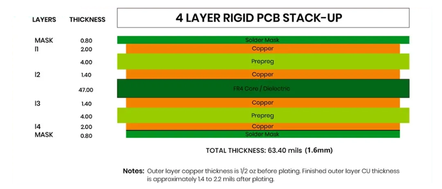
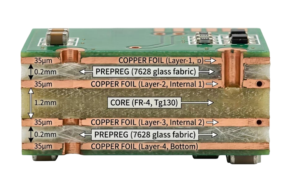
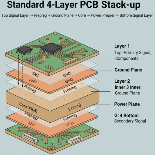
The standard 4 layer pcb stackup is Signal / Ground / Power / Signal on a 1.6mm FR-4 build, a ~1.2mm core between layers 2 and 3, bonded to the outer foils by two ~0.2mm prepreg layers.

That arrangement keep a continuous ground under the top signal layer, which is where return paths stay tight and impedance stays predictable. Another common stackup, Signal / Ground / Ground / Signal, uses two ground planes for the cleanest high-speed performance and routes power as copper pours on the outer layers.

4-layer PCB stackup cross-section: signal, ground, power and signal layers on a 1.6mm FR-4 build with prepreg and core dielectrics

The 4-Layer Stackup-to-Impedance Reference

LayerFunctionMaterialThicknessCopper
L1 (Top)Top layer — signal + componentsCopper foil35 µm1 oz
DielectricFR-4 prepreg~0.2 mm (7 mil)
L2Ground plane (gnd layer)Core (top)35 µm1 oz
CoreDielectric (Dk 4.0–4.8)FR-4 core~1.2 mm (42 mil)
L3 / Layer 4 pairPower plane (pwr layer / power rail)Core (bottom)35 µm0.5–1 oz
DielectricFR-4 prepreg~0.2 mm (7 mil)
L4 (Bottom)Bottom layer — signalCopper foil35 µm1 oz
Impedance Control

Impedance is governed by six variables: trace width, spacing, dielectric thickness, dielectric constant, copper thickness, and soldermask thickness, as detailed in a published multilayer lamination and impedance optimization patent. On a 4 layer pcb stackup 1.6 mm thick, a 50 Ω single-ended microstrip lands near 13 mil wide, with the copper pour held about two trace-widths (≈26 mil) away. A typical 4 layer pcb stackup follows standard 4 layer pcb design guidelines, while the best 4 layer pcb stackup for high-speed work swaps the power plane for a second ground.

50 Ω
Single-ended microstrip
13 mil
Trace width / 1.6 mm build
≈26 mil
Copper pour / ~2 trace-widths

Stackup Decision Matrix

StackupArrangementBest forTrade-off
SIG / GND / PWR / SIGGround L2, Power L3General mixed-signalWatch returns over power-plane splits
SIG / GND / GND / SIGTwo ground planesHigh-speed (DDR, USB, PCIe)Route power as outer copper pours
SIG / PWR / GND / SIGPower L2, Ground L3Power-dense, thicker current pathsHarder return-path management

Inside the 4-Layer Stackup

  1. The two internal layers (a continuous ground plane and a dedicated power layer or second gnd plane) give a 2-layer pcb no equivalent, that is the jump in routing density and component density.
  2. Route a 50 Ω microstrip on an outer layer or a stripline between planes; keep signal vias short and add ground stitching at layer transitions.
  3. For power electronics and high current, widen the pwr layer copper or pour power-and-ground planes on the outer layers (the stackup-with-ground option).
  4. A 4-layer board does not always need a dedicated power plane, designs with two ground planes and power routed on signal layers can outperform the textbook stackup for high-speed work.

4-Layer Design Rules We Check (DRC)

  1. Keep the ground and power plane pair continuous, no splits under high-speed traces, so the stack-up holds its reference.
  2. Place decoupling capacitors close to IC power pins, and plan component placement and the power distribution network early in your electronic design.
  3. Confirm trace width and spacing against our stack-up, export from KiCad, Altium, or any EDA tool and we run the design rules check.
  4. Let the inner planes shield RF and high-speed nets; the prepreg layers insulate each copper layer from the next.

PCBark 4-Layer PCB Capabilities: Specs, Materials, and Tolerances

PCBark is a manufacturer-direct fab, not a broker, so the capability matrix below is what our Huizhou line actually holds, with every value confirmable against your Gerber at quote time, under an ISO 9001 quality system.

Buyers get caught when a fab quotes a capability it cannot hold, the risk is a spec gap that surfaces only at production. Every value below is confirmable against your files, including the 4 layer pcb thickness in mm you need (standard 1.6 mm, range 0.3–6.0 mm).

PCBark 4-Layer PCB Fabrication Capabilities and Precision Standards

Confirmed Capability Matrix // Huizhou Line

  • Layer count
    4 (IPC-6012F Type 3 / Type 4 with blind-buried vias)
  • Base material
    FR-4, high-Tg FR-4, thermal aluminum substrate
  • Finished thickness
    0.3–6.0 mm (standard 1.6 mm)
  • Copper weight
    0.5–6 oz (standard 1 oz outer)
  • Min trace / space
    3 mil / 3 mil (0.075 mm)
  • Surface finish
    ENIG, lead-free HASL, HASL, OSP, immersion gold
  • Controlled impedance
    50 Ω single-ended, 90/100 Ω differential, ±10% (±5% on request)
  • Build class
    IPC-6012F Class 2 and Class 3
  • Solder mask / legend
    LPI mask (green/white/red/black), inkjet legend
  • Volume
    Quick-turn prototype to high-volume production

Authorized Statement

"We publish the stackup we actually build, not a catalog page. When a customer needs 50 ohm on a 1.6mm board, we hand them the prepreg and core values from the panel we'll run, then prove it with a coupon."

Authorized Sign-off By PCBark Engineering Team

Controlled Impedance and In-House Verification

Controlled impedance means the fab tunes trace geometry and dielectric to hit a target, typically 50 Ω single-ended or 90–100 Ω differential, and then tests it. PCBark verifies impedance with a TDR-driven coupon on every controlled-impedance order.

Engineers regularly see a big difference between a fab's generic controlled impedance calculator and their EDA tool. Resin content and glass-weave skew shift the dielectric constant away from catalog values, so that gap is real. We compute your target against our panel's actual dielectric, then confirm it on a TDR test coupon, so the delivered board matches the math, the same controlled-impedance via engineering documented in USPTO filings.

The honest version

Realistic impedance tolerance on a 4-layer board is ±10%, and ±5% is achievable on request with tighter process control. We will not claim a tighter number without coupons or our own dielectric data.
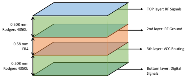
Engineering render of 4-layer PCB core stack with controlled impedance lines TDR VERIFIED

The PCBark Impedance Verification Stack

  • 01

    Impedance tester (TDR)

    Every controlled-impedance lot ship with a measured coupon, not a calculated estimate.

  • 02

    X-Ray inspection

    Registration and via integrity through all four layers.

  • 03

    Metallurgical microscope

    Micro-section confirms layer-to-layer alignment and plated copper.

  • 04

    Copper metrology

    Hole-copper (UK Oxford) and surface-copper thickness (German Fischer) gauges.

4-Layer PCB Manufacturing Process: In-House, IPC Class 2/3

A standard 4 layer pcb is built in a single lamination cycle: the two inner layers are imaged on a core, then bonded to the outer foils in one press, sequential lamination is only needed for blind or buried vias.

This is the cost reality buyers miss: layer count is not the main cost driver, lamination cycles are. A single-cycle 4-layer board stays close to 2-layer economics, while any sequential-lamination build (extra vias) is what truly raises cost, that is the trade-off worth understanding.

4-Layer PCB Cross-Section Lamination Build Path
FIG 01. CROSS-SECTION

The PCBark Single-Lamination Build Path

  • STEP.01
    Inner-layer imaging & etch LDI laser direct imaging defines L2/L3 circuitry.
  • STEP.02
    Oxide treatment Roughens inner copper for lamination adhesion.
  • STEP.03
    Lamination (single cycle) Prepreg + core + foils pressed under heat and pressure (resin-control lamination patent).
  • STEP.04
    Drilling German Schmoll and CNC drills bore through-holes, vias, and component holes from your Gerber file data.
  • STEP.05
    PTH copper deposition + plating Through-hole walls plated to IPC-6012 minimums.
  • STEP.06
    Outer-layer imaging & etch Defines L1/L4 traces and pads.
  • STEP.07
    Solder mask Silkscreen legend + ENIG/HASL finish, protection, marking, and a solderable surface.
  • STEP.08
    CNC profiling + AOI X-Ray, flying-probe, impedance-coupon test.

IPC-6012F Class 2 vs Class 3, What Changes

Acceptance criterion Class 2 (industrial) Class 3 (high-rel)
Plated through-hole wall copper (avg) 20 µm 25 µm
Min external annular ring 50 µm 50 µm (no 90° breakout)
Through-hole barrel solder fill ≥50% ≥75%
Max conductor-width reduction 30% 20%
Thermal stress / solder float 288 °C / 10 s (IPC-6012 §3.6.1)
Your build class is locked before fabrication and cannot be upgraded after the fact, so we confirm Class 2 or Class 3 at quote, automotive and medical work routes to Class 3 and the matching IPC-6012EA / EM addenda.

From Bare Board to Turnkey: Assembly, Sourcing, and DFM

Clean prototypes do not prove production readiness, yield and process variation only show up at scale. PCBark closes that gap with front-end DFM and a single-source path from 4-layer fabrication into SMT assembly.

Incomplete data is the most common sourcing failure: when stackup, copper weight, impedance targets, or drill data are missing, the supplier guesses or stalls. Our proactive DFM review catches clearance and trace-width issues before the panel run, so the job does not pause mid-stream.

4-Layer DFM & RFQ Checklist

  • NODE 01

    Stackup with target impedances (single-ended and differential).

  • NODE 02

    Copper weight per layer and finished board thickness.

  • NODE 03

    Surface finish (ENIG / HASL / OSP) and IPC build class.

  • NODE 04

    Drill table, minimum trace/space, and controlled-impedance net list.

Yamaha SMT placement and 3D solder-paste inspection traceability

> Specification_Extension

For turnkey orders we extend the same traceability into assembly: Yamaha SMT placement, 3D solder-paste inspection, AOI, and X-Ray for BGA, with components pulled through authorized distributors (Arrow, Avnet, DigiKey) and assembled to IPC-A-610 Class 2/3. One partner owns the chain from fabrication to a tested board, with trace-defect controls of the kind described in recent PCB fabrication patents. From a quick-turn PCB prototype to high-volume PCB production, the same line runs your PCB assembly, and every finished PCB board is electrically tested before it ships, the insulating layers (prepreg and core) stay intact through every step, and design-for-manufacturability checks confirm the board carries its electronic components reliably.

Quality, Certifications, and Reliability

Trust on an offshore order comes from auditable systems, not slogans, so every PCBark board ships against documented certifications and a full inspection chain.

PCBark has manufactured printed circuit boards since 2010 and serves more than 2,000 global end-users, with over 95% of output exported. Over 16 years, that record neutralizes the risk of an anonymous quote and the hidden cost of a failed audit. A verifiable certificate set is what separates a manufacturer-direct fab from a broker.

IATF 16949

Automotive QMS

UL

Listed (since 2014)

ISO 9001

Quality (since 2011)

ISO 14001

Environmental

CE

Conformity

RoHS / REACH

Materials compliance

PROCESS & INSPECTION

Inspection is layered, not assumed: AOI scans trace width and spacing, X-Ray checks registration and BGA joints, and flying-probe or fixture testing verifies every net, all under ISO 9001 and ISO 14001 systems. Our zero-defect target backs every shipment.

CONTINUOUS VERIFICATION FEED: AOI SCAN MODE

LIVE SYNC
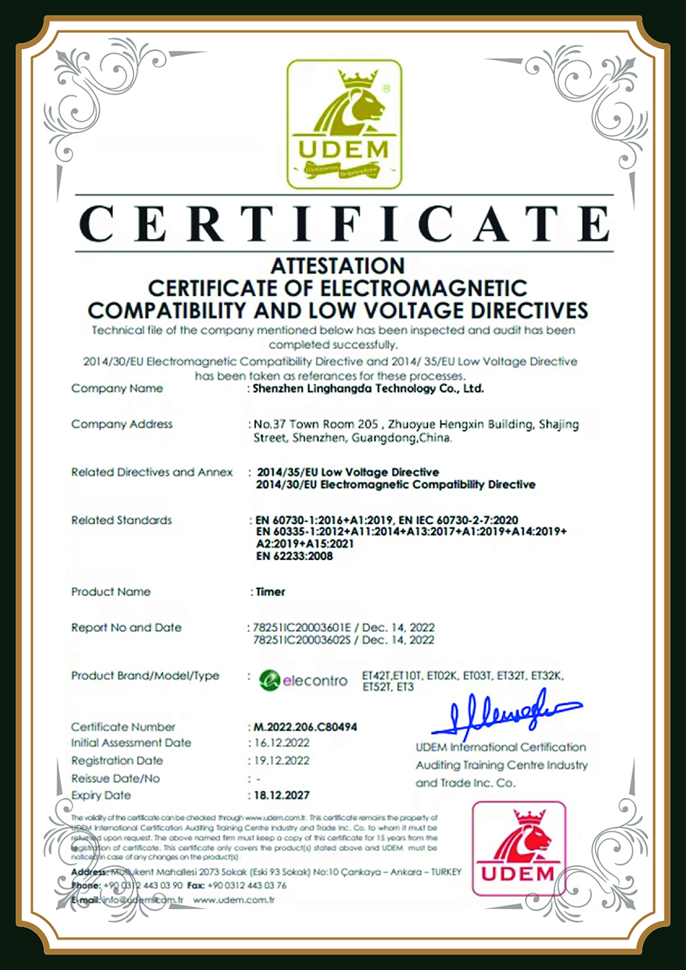
CE Mark Certification
IATF 16949 Certification
ISO 9001 Assembly Certification
ISO 14001 Assembly Certification
ISO 14001 PCB Certification
ISO 9001 PCB Certification
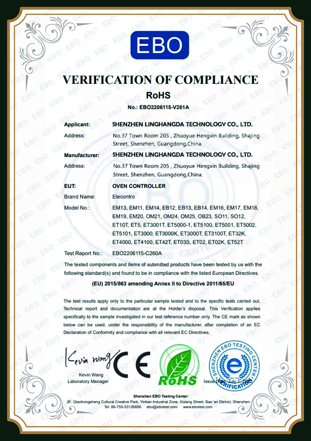
RoHS Compliance
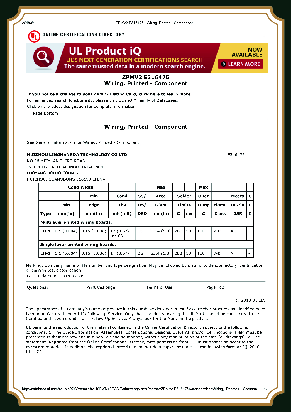
UL 94V-0 Certification

Cost, Lead Time, and Total Cost of Ownership

Headline board price is the smallest line on a 4-layer order, shipping and customs usually dwarf it. The cost that matter is the landed, all-in total, and how predictable it is.

Real buyer orders show the trap clearly: a recent US order billed roughly $9 for the board but $38 in shipping and $16 in customs duties, and another saw a $200 broker fee held against a $500 order. Buyers vent that the US PCB market can mean arbitrarily high domestic prices, which pushes them offshore into exactly these hidden fees, duties set by the US Harmonized Tariff Schedule. Quoted quick-turn also stretches to three weeks door-to-door once customs clears.

Precision 4-Layer PCB cross-section trace layout
Precision 4-Layer PCB internal routing and components

What Actually Drives 4-Layer PCB Cost

  • Lamination cycles (blind/buried vias) Largest driver — sequential lamination, not layer count
  • Copper weight 2–3 oz adds ~30–50% material cost vs 1 oz
  • Base material High-Tg / specialty laminate above standard FR-4
  • Surface finish ENIG / immersion gold above HASL / OSP
  • Order quantity Per-unit cost drops sharply from prototype to volume

Board cost ≈ smallest line item

On many offshore 4-layer orders, shipping + customs exceed the board price several times over. A manufacturer-direct quote with transparent, all-in cost removes that surprise.

On total cost of ownership, the layer-count premium often pays for itself: a 4-layer board can remove the external filter or extra connectors a noisy 2-layer design would need, lowering the overall bill of materials. Choosing suppliers on price alone is the most expensive mistake, late, failing, or rework-heavy boards erase the saving.

The honest trade-off: the 2 layer vs 4 layer pcb cost gap is real at prototype (about 3–5×) but narrows to roughly 2–3× at volume, and a cleaner 4-layer board often lowers the total bill of materials anyway.

Source: documented buyer orders (industry forums, 2024–2025). Your landed total depends on volume, spec, and destination.

Frequently Asked Questions

01

How much does a 4-layer PCB cost?

There is no single fixed price. Prototype runs of 1–10 boards typically land around $25–$150 per unit, medium runs around $8–$40, and volume orders fall to roughly $3–$8 per unit. Cost is driven by size, copper weight, material, finish, and whether blind or buried vias force extra lamination, request a quote with your stackup for an exact figure.

02

What is the standard 4-layer PCB stackup and thickness?

The standard build is Signal / Ground / Power / Signal on a 1.6mm FR-4 board, a ~1.2mm core between the two inner planes, bonded to the outer copper foils by two ~0.2mm prepreg layers. Thinner (1.0mm) and thicker (up to 6.0mm) options are available depending on your mechanical and impedance needs.

03

Can you actually hold controlled impedance on a 4-layer board?

Yes. Realistic tolerance is ±10% (±5% on request), and we hit it by computing your target against our panel's actual dielectric values, then verifying it on a TDR test coupon. Community guidance is right that 2-layer boards cannot give good impedance control, go 4-layer, and insist the fab tests those traces against your 50 Ω or differential target.

04

Will my 4-layer PCB need more than one lamination cycle?

A standard 4-layer board is built in a single lamination cycle. You only need sequential lamination if your design includes blind or buried vias. Back-drilling or resin-filled vias add steps but are not extra lamination cycles, and a single-cycle build keep cost close to 2-layer economics.

05

What surface finishes and copper weights can I choose?

Surface finishes include ENIG, lead-free HASL, HASL, OSP, and immersion gold. Copper weight runs from 0.5 oz to 6 oz, with 1 oz outer as the standard; heavier copper (2–3 oz) raises material cost and changes trace geometry, so we tune trace width to keep impedance on target.

06

What is the real lead time, including shipping and customs?

Fabrication turnaround can be quick-turn to about 10 days for a 4-layer board, but plan for the door-to-door total. Offshore orders routinely stretch to three weeks once customs clears, and tariff or broker fees can add unexpected cost. We quote an all-in lead time so the schedule is predictable.

07

Do you build to IPC Class 2 or Class 3?

Both. Class 2 suits industrial, communications, and computing products; Class 3 covers medical, automotive, and high-reliability work with tighter copper, annular-ring, and barrel-fill requirements. Your class is locked before fabrication and cannot be upgraded afterward, so we confirm it at quote time.

08

Can you handle assembly, not just the bare board?

Yes, we offer turnkey 4-layer fabrication plus SMT assembly under one supplier. That includes Yamaha placement, solder-paste inspection, AOI, X-Ray for BGA, and component sourcing through authorized distributors, assembled to IPC-A-610 Class 2/3 with full traceability from board to tested unit.