
Get in touch with PCBark Company

Multilayer Flex PCB (4-12 Layer)
Multilayer Flex PCB (4–12 Layer) — Custom FPC Manufacturer
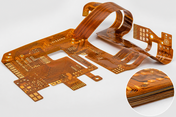
Stack three or more copper layers into a single bendable circuit, without the connector failures of stacked rigid boards. PCBark manufactures multilayer flex PCBs from 4 to 12 layers on polyimide, with ±10% impedance control and a 1,000,000-cycle bend life on dynamic designs.
- 4–12
Conductive layers
- 1M
Bend cycles (dynamic)
- 38μm
Min line / space
- ±10%
Impedance control
- Class 3
IPC-6013 build
- No MOQ
Proto to volume
When Double-Sided Flex Runs Out of Routing Room
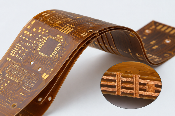
A multilayer flex PCB – a flexible printed circuit board (FPCB) that contains three or more layers of copper conductors – is created by laminating the copper layers onto a flexible substrate, most commonly polyimide. These layers are interconnected using plated-through holes, microvias, or blind and buried vias. This configuration offer the benefits of a flexible printed circuit (bendability) combined with the high-density routability of a multilayer printed circuit board (where single-sided or double-sided flex boards would run out of space).
01
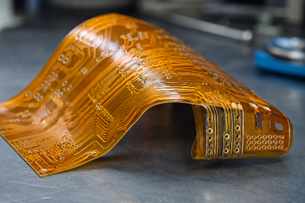
Where two copper layers run out
Once a double-sided flex circuit board reaches capacity, the designers often must route crossovers and place additional components, such as controlled impedance lanes and shields, on more than two copper layers. This usually leads to stacking more rigid circuit boards with ribbon cables. Their shared problem is a higher risk of connector failure in the field.
02
The counterintuitive part most spec sheets skip
It’s a misunderstanding that more layers is somehow equal to “more flexibility.” Instead, multilayer flex is ideal for static or high-density applications where a flexible PCB is bent once to fit, and then holds that position. For truly dynamic applications requiring repeated flexing (like a hinge or a printer head), more flexible design approaches with fewer layers and the use of rolled-annealed copper are generally more suitable.
Process & Standards
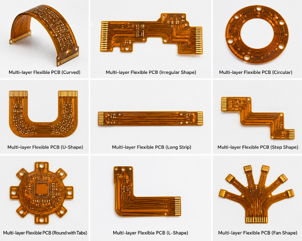
Flexible circuits span from simple single-layer builds and single-sided flex PCBs, through double-sided designs, to multi-layer flex PCBs configurations-and the core decision between them hinges on those tradeoffs, which this page details. Our engineers calculate the flex stackup based on your specific motion profile, then verify its integrity against IPC-6013 acceptance criteria before it ships.
PCBark Multilayer Flex PCB Capabilities & Stackup
Be wary of a flex quote that promises a “capability” but delivered it only as a one-off in a lab, not as a production spec. Every parameter below reflects our in-house flexible PCB manufacturing capacity at PCBark, managed under ISO 9001 and IATF 16949 process control across 16 years and 37 flex lines. Our finest line and space is an industry-leading 38 microns — better than the 50-micron capability other houses claim — so our PCB design team holds a high-density 8- to 12-layer multilayer flexible circuit board to tight tolerance.
CAPABILITY MATRIX
LIVE SPEC
- Conductive layers 1L – 12L
- Board thickness 0.10mm – 0.80mm+
- Polyimide film 12.5μm – 50μm (DuPont Pyralux AP class)
- Copper weight 1/3 oz – 2 oz (RA or ED)
- Min line / space 38μm (1.5 mil)
- Min laser via 0.075mm (3 mil)
- Impedance control ±10% (±5–7% for Class 3)
- Max panel size 250mm × 1000mm+
- Surface finish ENIG, Hard Gold, OSP, Immersion Tin
- Stiffeners FR4, polyimide, aluminum, stainless
How a 4 layer flex pcb stackup holds together
We ensure symmetric 4-layer construction-FCCL + adhesive + flex core + adhesive + FCCL-for optimal warpage control during the high-temperature lamination process. For more complex constructions, we use a “bookbinder” approach where outer flex layers are slightly extended, so the multilayer flex circuit folds cleanly within the inner structure without overstraining the inner conductors. Profiles use precise laser cutting, so dense outlines stay within tolerance.
Design note from our DFM desk
We orthogonally route adjacent layer signals to block crosstalk, and isolate the bend area from vias and pads. As a rule of thumb, for a PCB stack, an extra layer of copper adds about 0.0055” in thickness, defining your design’s required minimum bend radius.
Get Instant QuoteHow Many Layers Do You Need? Layer-Count Selection Matrix
Layer count is not only a routing-efficiency decision for your flex circuit board — it also drives overall cost and signal integrity. This matrix outlines the decisions our design engineers take for each flex quote, providing practical bend radii and lead times rather than vague qualifiers like “low,” “medium,” or “high.”
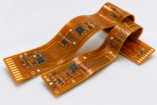
| Layers | Best-fit use | Impedance need | Min bend radius | Relative cost | Lead time |
|---|---|---|---|---|---|
| 4L | Control + signal split, compact modules | Single-ended | ~10× thickness | Base | 2 wks |
| 6L | Mixed analog/digital, light RF | ±10% diff pairs | ~12× thickness | +25–40% | 2–3 wks |
| 8L | High-speed digital, dense BGA fan-out | ±7% controlled | ~12–15× thickness | +50–70% | 2–3 wks |
| 12L | Max density, multi-rail power + RF | Class 3 ±5% | 15×+ thickness | +90–120% | 3 wks |
Multilayer Flex PCB vs Rigid-Flex PCB, Which Fits Your Design
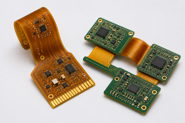
Pure vs Rigid-Flex These two aren’t ranked best-to-worst; they solve different mechanical problems. A pure multilayer flex keeps the whole board bendable; a rigid-flex PCB bolts rigid component zones to flexible interconnect ribbons (rigid-flex fabrication, WO2018132603A1).
SPECIFICATION MATRIX
| Attribute | Multilayer Flex PCB | Rigid-Flex PCB |
|---|---|---|
| Layer range | 4 – 12 (all flex) | 4 – 20+ (rigid + 1–6 flex) |
| Base material | Polyimide only | FR4 + polyimide |
| Component support | Needs stiffeners | Native rigid zones |
| Relative cost | Lower | +30–60% |
| Best for | All-bendable, space-critical | 3D folded assemblies, heavy parts |
How PCBark Engineers Reliability into Every Multilayer Flex PCB
Reliability in flex is won at the copper and the lamination, not in the data sheet. The single biggest dynamic-life lever is copper type: without rolled-annealed (RA) copper, dynamic flex circuits typically fail within 500-1,000 cycles-far below the 10,000+ cycles most moving applications demand.
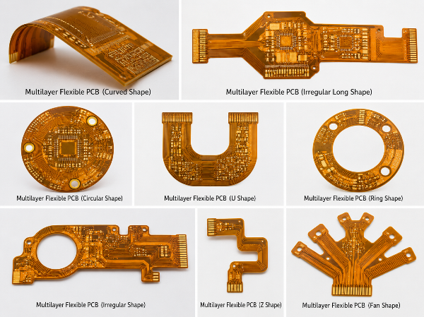
We specify RA copper and adhesiveless cast-polyimide laminate for any board that moves (flex copper-and-bend construction, US6927344B1), then validate it. Our dynamic builds clear 1,000,000 bend cycles, and impedance shifts stay under 5% as long as the bend radius exceeds ten times circuit thickness.
Delamination is the most common flex failure at reflow, and its root cause is moisture absorbed by the polyimide. We ship in humidity-controlled, moisture-barrier packaging and supply pre-bake profiles, then verify the build holds under 100 thermal shocks with under 5% resistance change.
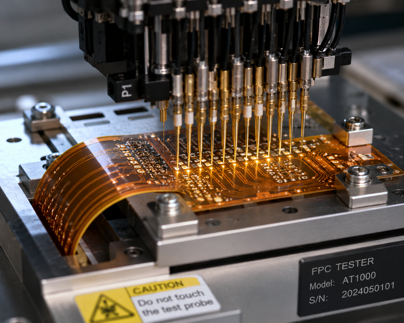
Every build is verified in-house – AOI, X-ray, and impedance test on PCBark’s ISO 9001 line – because reliability you cannot measure is reliability you cannot ship. Unlike a broker that drop-ships a polyimide PCB, we own the process from lamination to test across 16 years of multilayer flex circuits.
Those choices map straight to where these flexible PCBs live:
Places where a field failure is far more expensive than the board.
- Medical devices like MRI and imaging probes
- Aerospace avionics modules
- Automotive ADAS sensors
- 24/7 wearables
On dynamic boards we never quote ED copper to save a few cents. We have watched 0.5-ounce rolled-annealed copper outlast electrodeposited by orders of magnitude on the same bend jig, that’s the difference between a 1-million-cycle hinge and a warranty return.
PCBark Flex Engineering TeamCertifications & Compliance
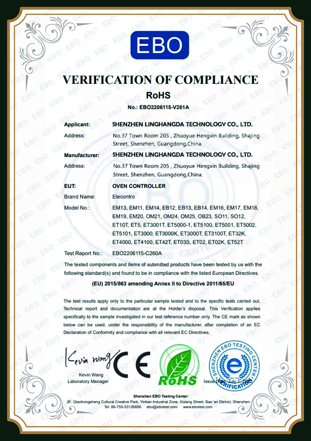
For an overseas buyer, certs are the layer of trust that a spec table can’t substitute. All multilayer flex PCBs are built to spec standards and supported by audited quality systems—documentation travels with your job.
CRITICAL NOTE: CLASS 3 SPEC
Class 3 isn’t free. A Class 3 flex build costs 40 to 80% more than a Class 1 board — inspection and testing are dramatically stricter across the process. PCBark matches the class to your needs so you’re not paying for a blanket increase in reliability.
STANDARD ID COVERAGE SCOPE
- IPC-6013 Class 2 / Class 3 flex
- IPC-2223 Flex design spec
- ISO 9001 Quality system
- IATF 16949 Automotive
- ISO 14001 Environmental
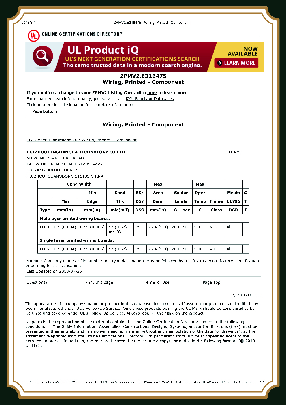
- UL 94V-0 Flammability
- RoHS / REACH Material compliance
● LIVE
CONTINUOUS VERIFICATION FEED: AOI SCAN MODE






Ordering Your Multilayer Flex PCB, Lead Time, DFM & Quote
As a full-service flex PCB provider, PCBark runs DFM review, component sourcing, flex and multilayer PCB fabrication, and full board assembly, testing, and kitting under our ISO 9001 quality system, all under one roof with zero MOQ. Flex prototypes ship in 3-7 business days; multilayer and rigid-flex ship in 2-3 weeks including testing.
What actually drives your flex PCB price
Flex pricing is a stack of inputs, not one number. Knowing the main cost drivers up front keeps your quote honest and transparent:
| Cost driver | Effect on price |
|---|---|
| Layer count | Each pair adds lamination + via steps |
| Laser-drilled vias | More microvias = more drill time |
| Impedance-controlled layers | Tighter tolerance = added test |
| IPC class | Class 3 vs Class 1 = +40–80% |
| Surface finish | Hard gold > ENIG > OSP |
Before you request a quote
Send us your Gerber and BOM, plus any specs including the minimum bend radius, and flag the bend zones on the drawing. Our flex DFM engineering team optimizes your flexible PCB design — panelization, stack-up symmetry, and the flex PCB connector tail.
75% / 70%
Industry data shows a single integrated flex circuit can cut weight up to 75% and connection cost up to 70% versus traditional point-to-point wiring and connectors.
Source: Minco flex circuit design data. Actual results vary by design — request a custom analysis.


